Technische Universit¨ at M¨ unchen
Max-Planck-Institut f¨ ur Physik
Investigation of Properties of Novel Silicon Pixel Assemblies
Employing Thin n-in-p Sensors and 3D-Integration
Philipp Weigell
Vollst¨ andiger Abdruck der von der Fakult¨ at f¨ ur Physik der Technischen Universit¨ at M¨ unchen zur Erlangung des akademischen Grades eines
Doktors der Naturwissenschaften genehmigten Dissertation.
Vorsitzender: Univ.-Prof. Dr. Martin Beneke Pr¨ ufer der Dissertation:
1. Hon.-Prof. Dr. Siegfried Bethke 2. Univ.-Prof. Dr. Stephan Paul
Die Dissertation wurde am 20.12.2012 bei der Technischen Universit¨ at M¨ unchen eingereicht
und durch die Fakult¨ at f¨ ur Physik am 15.01.2013 angenommen.
Abstract
Until the end of the 2020 decade the LHC programme will be defining the high energy frontier of particle physics. During this time, three upgrade steps of the accelerator are currently planned to further increase the luminosity and energy reach. In the course of these upgrades the specifications of several parts of the current LHC detectors will be exceeded. Especially, the innermost tracking detectors are challenged by the increasing track densities and the radiation damage. This thesis focuses on the implications for the ATLAS experiment. Here, around 2021/2, after having collected an integrated luminosity of around 300 fb −1 , the silicon and gas detector components of the inner tracker will reach the end of their lifetime and will need to be replaced to ensure sufficient performance for continued running—especially if the luminosity is raised to about 5 · 10 35 cm −2 s −1 as currently planned. An all silicon inner detector is foreseen to be installed. This upgrade demands cost effective pixel assemblies with a minimal material budget, a larger active area fraction as compared to the current detectors, and a higher granularity. Furthermore, the assemblies must be able to withstand received fluences up to 2 · 10 16 n eq /cm 2 .
A new pixel assembly concept answering the challenges posed by the high instantaneous luminosities is investigated in this thesis. It employs five novel technologies, namely n-in-p pixel sensors, thin pixel sensors, slim edges with or without implanted sensor sides, and 3D-integration incorporating a new interconnection technology, named Solid Liquid InterDiffusion (SLID) as well as Inter-Chip-Vias (ICVs).
n-in-p sensors are cost-effective, since they only need patterned processing on one side. Their performance before and after irradiation is investigated and compared to results obtained with currently used n-in-n sensors. Reducing the thickness of the sensors lowers the amount of multiple scattering within the tracking system and leads to higher charge collection efficiencies after irradiation. Devices with thicknesses between 75 µm and 150 µm are investigated before and after irradiation with different experimental approaches, namely radioactive sources, beam tests, and laser measurements. The obtained results are compared to those gathered for devices using the currently widely used thickness of 285 µm. By implanting the sides of the sensors, the distance between the last active pixel implant and the edge can be considerably reduced, allowing for a compact module concept. In this thesis several steps are discussed to reduce this distance from 1.1 mm down to 50 µm. Subsequently, the performance of the different implementations is investigated. The SLID interconnections offer the possibility to stack sensors and several layers of read-out electronics as well as a reduced minimal pitch and eventually a lower cost. In combination with ICVs it paves the way to 3D-integrated pixel assemblies.
These can be further optimised in terms of the active area, thanks to a reduced footprint of the read-out chip. Furthermore, it enables the use of specialised processes for the analogue and digital parts of the read-out chip in the different layers. First assemblies employing SLID interconnections were built and the properties of the interconnection are discussed. Finally, etching of ICVs was started and the present status is reviewed.
Keywords: ATLAS, Pixel detector, HL-LHC, n-in-p, Thin sensors, 3D-integration, Radiation
damage
Zusammenfassung
Das LHC-Programm wird bis Ende der 2020er-Jahre Vorreiter in der Hochenergiephysik sein.
Bis dahin sind derzeit drei Ausbau- und Erweiterungstufen des Beschleunigers geplant, die den Luminosit¨ ats- und Energiebereich erweitern. Im Zuge dieser Erweiterungen werden die Spezifikationen vieler Teile der LHC-Detektoren ¨ uberschritten werden. Insbesondere die innersten Spurdetektoren werden durch die erh¨ ohten Spurdichten und entstehenden Strahlensch¨ aden beansprucht. In dieser Dissertation liegt der Schwerpunkt auf den Auswirkungen f¨ ur das ATLAS-Experiment. Um 2020/1, nachdem um 300 fb −1 integrierte Luminosit¨ at gesammelt sein wird, erreichen die Silizium- und Gas-Detektoren des inneren Spurdetektors das Ende ihrer Lebenszeit und m¨ ussen ersetzt werden. Dadurch soll eine ausreichende Leistung f¨ ur die weitere Laufzeit gew¨ ahrleistet werden – insbesondere, wenn, wie derzeit geplant, die Luminosit¨ at auf n¨ aherungsweise 5 · 10 35 cm −2 s −1 angehoben wird. Hierbei ist vorgesehen, einen rein auf Silizium basierten Detektor einzusetzen. F¨ ur diesen Ausbau werden, verglichen mit den derzeitigen Detektoren, kosteng¨ unstige Pixelmodule mit minimalem Materialeinsatz, einem gr¨ oßeren aktiven Fl¨ achenanteil und einer h¨ oheren Granularit¨ at ben¨ otigt. Des Weiteren m¨ ussen die Module Strahlendosen bis zu 2 · 10 16 n eq /cm 2 standhalten k¨ onnen.
Als L¨ osung f¨ ur die sich aus der hohen instantanen Luminosit¨ at ergebenden Anforderungen wird in dieser Dissertation ein neues Pixelmodulkonzept erforscht. Dabei kommen f¨ unf neue Technologien zum Einsatz: n-in-p-Pixelsensoren, d¨ unne Sensoren, schmale Randzonen sowohl mit als auch ohne implantierte Sensorseiten sowie 3D-Integration. Die 3D-Integration setzt sich zusammen aus einer neuen Verbindungstechnologie, genannt Solid Liquid InterDiffusion (SLID), und Inter-Chip-Vias (ICVs).
n-in-p-Sensoren sind kosteng¨ unstig, da sie nur auf einer Seite strukturiert prozessiert werden m¨ ussen. Ihre Eigenschaften vor und nach Bestrahlung werden erforscht und mit Ergebnis- sen der derzeit verwendeten n-in-n-Sensoren verglichen. Die verringerte Sensordicke reduziert Vielfachstreuung im Spurdetektorsystem und f¨ uhrt zu h¨ oheren Ladungssammlungseffizienzen nach Bestrahlung. Sensoren mit Dicken zwischen 75 µm und 150 µm werden vor und nach Bestrahlung mit verschieden experimentellen Ans¨ atzen erforscht, z. B. mit Strahltests, Mes- sungen mit radioaktiven Quellen und Lasern. Zum Vergleich werden Ergebnisse f¨ ur Sensoren mit der heute gebr¨ auchlichen Sensordicke von 285 µm herangezogen. Durch Implantieren der Sensorseiten, kann der Abstand zwischen dem letzten aktiven Pixelimplantat und der Kante d edge entscheidend verkleinert werden und damit das Pxielmodul kompakter gemacht werden. In dieser Dissertation, werden verschiedne Schritte vorgestellt, die es erm¨ oglichen, d edge von 1,1 mm auf 50 µm zu verkleinern. Anschließend wird die Eignung der verschiedenen Ans¨ atze unter- sucht. Die SLID-Verbindungen erm¨ oglichen neben der Schichtung von Sensoren- und mehrerer Ausleseelektroniklagen eine erh¨ ote Granularit¨ at und sind g¨ unstiger. In Kombination mit ICVs ebnet dies den Weg f¨ ur 3D-integrierte Pixelmodule. Dank des reduzierten Fl¨ achenbedarfs der Auslese, verbessert sich der aktive Fl¨ achenanteil dieser Pixelmodule weiter. Weiter erm¨ oglichen sie die Nutzung spezieller Prozesse f¨ ur analoge und digitale Bereiche in den verschiedenen Lagen der Ausleseelektronik. Erste Module mit SLID-Verbindungen wurden hergestellt und die Eigenschaften der Verbindung werden besprochen. Schlussendlich wurde das ¨ Atzen von ICVs gestartet und der aktuelle Stand wird dargestellt.
Schlagw¨ orter: ATLAS, Pixeldetektor, HL-LHC, n-in-p, d¨ unne Sensoren, 3D-Integration,
Strahlensch¨ aden
F¨ ur Eva
Contents
1 Upgrade Plans for the Large Hadron Collider and the ATLAS Detector 1
1.1 Physics Motivation . . . . 1
1.1.1 Higgs Mechanism . . . . 1
1.1.2 Supersymmetry . . . . 2
1.1.3 Further Beyond the Standard Model . . . . 2
1.2 From LHC to HL-LHC . . . . 2
1.2.1 The LHC Accelerator Complex . . . . 2
1.2.2 Luminosity . . . . 4
1.2.3 Current Performance . . . . 5
1.2.4 Upgrade Roadmap . . . . 6
1.3 ATLAS . . . . 7
1.3.1 The ATLAS Pixel Detector . . . . 9
1.3.2 Upgrade Roadmap . . . . 10
1.4 The MPP/MPI-HLL Pixel Assembly Concept . . . . 12
1.4.1 n-in-p Sensors . . . . 13
1.4.2 Thin Sensors . . . . 13
1.4.3 3D-Integration . . . . 14
1.4.4 Slim and Active Edges . . . . 14
1.4.5 Intermediate Designs for the R&D Process . . . . 15
2 Theory of Radiation Hard Pixel Detectors 17 2.1 Physical Foundations . . . . 17
2.1.1 Intrinsic and Extrinsic Semiconductors . . . . 18
2.1.2 The pn-Junction . . . . 18
2.1.3 Charge Generation . . . . 20
2.1.4 Charge Carrier Transport . . . . 21
2.2 Radiation Damage . . . . 21
2.2.1 Bulk Defects . . . . 22
2.2.2 Charge Multiplication . . . . 25
2.3 Basic Design Considerations . . . . 25
2.3.1 Special Structures . . . . 25
2.3.2 Bulk Materials . . . . 27
3 Methodology 29 3.1 Measurement of IV Characteristics . . . . 29
3.2 PHEMOS . . . . 29
3.3 Irradiation Sites . . . . 30
3.4 ALiBaVa Readout System . . . . 31
3.4.1 Instrumentation . . . . 31
3.4.2 Data Acquisition and Analysis Chain . . . . 33
3.4.3 Uncertainties . . . . 34
3.5 Edge-TCT . . . . 36
3.5.1 Instrumentation and Data Acquisition . . . . 36
3.5.2 Analysis Chain . . . . 37
3.5.3 Uncertainties . . . . 38
3.6 Operation of ATLAS Read-Out Chips . . . . 39
3.6.1 ATLAS Read-Out Chips . . . . 40
3.6.2 USBPix Read-Out-System . . . . 42
3.6.3 Tuning . . . . 43
3.7 Beam Test . . . . 46
3.7.1 Beam-Lines . . . . 46
3.7.2 Instrumentation . . . . 46
3.7.3 Analysis Chain . . . . 48
4 n-in-p Pixel Detectors 51 4.1 CiS Production . . . . 51
4.1.1 Sensor Design . . . . 51
4.1.2 Post-Processing at IZM . . . . 53
4.2 Properties Before Irradiation . . . . 55
4.2.1 IV Characteristics . . . . 55
4.2.2 Assembly Tuning . . . . 57
4.2.3 Charge Collection and Sharing . . . . 59
4.2.4 Spatial Resolution . . . . 64
4.2.5 Hit Efficiency . . . . 65
4.3 Properties After Irradiation . . . . 67
4.3.1 Overview of Irradiated Assemblies . . . . 67
4.3.2 Electrostatic Properties . . . . 67
4.3.3 Assembly Tuning . . . . 69
4.3.4 Charge Collection and Sharing . . . . 70
4.3.5 Spatial Resolution . . . . 73
4.3.6 Hit Efficiency . . . . 77
4.4 Conclusion . . . . 78
5 Thin Sensors 79 5.1 Thin Sensor Productions . . . . 79
5.1.1 Processing of Thin Sensors . . . . 79
5.1.2 SOI1 Production . . . . 80
5.1.3 SOI2 Production . . . . 81
5.1.4 VTT Production . . . . 83
5.2 Charge Collection of Strip Sensors . . . . 84
5.2.1 Investigated Structures . . . . 85
5.2.2 Induced Current Pulse Shapes . . . . 85
5.2.3 Charge Collection Profile . . . . 88
5.2.4 Charge Collection Efficiency . . . . 88
5.3 Properties of Thin Pixel Sensors . . . . 91
5.3.1 IV Characteristics and Irradiation Programme . . . . 92
5.3.2 Assembly Tuning . . . . 95
5.3.3 Charge Collection and Sharing . . . . 101
5.3.4 Spatial Resolution . . . . 110
5.3.5 Hit Efficiency . . . . 111
5.4 Conclusions and Outlook . . . . 114
6 3D-Integration: SLID and ICV 117 6.1 Solid Liquid Interdiffusion . . . . 117
6.1.1 Alignment . . . . 118
6.1.2 Mechanical Strength . . . . 121
6.1.3 Interconnection Efficiency . . . . 122
6.2 ICV . . . . 125
6.3 Conclusions . . . . 126
7 Conclusions and Outlook 129
List of Abbreviations and Acronyms 131
List of Figures 133
List of Tables 137
Bibliography 139
Overview
A novel pixel assembly concept for high energy physics experiments at high luminosity hadron colliders is investigated. It incorporates five new technologies, namely n-in-p sensors, thin sensors, slim edges with or without implanted sensor sides, and 3D-integration incorporating a new interconnection technology, named Solid Liquid InterDiffusion (SLID) as well as Inter-Chip-Via (ICVs).
Chapter 1: After a physics motivation the LHC and the ATLAS detector as well as their upgrade roadmaps are discussed together with the resulting challenges and requirements on the individual detector parts. In the last section the investigated assembly concept is introduced as an answer to the challenges posed to the pixel part of the inner tracking detector.
Chapter 2: An introduction into semiconductor physics is given up to the level of detail needed for the investigations presented in the following chapters. Especially, the effects of radiation damage for silicon sensors are highlighted.
Chapter 3: Novel n-in-p pixel detectors are assessed in terms of operational performance before and after irradiation. In addition, their properties are compared to the currently used n-in-n pixel detectors.
Chapter 4: Thin strip and pixel detectors are investigated and their operational requirements are determined with a focus on quantities that are most relevant for high energy physics experiments as for example the collected charge to threshold ratio and the hit efficiency.
Chapter 5: The reach of the SLID interconnection technique is discussed along results derived from pixel assemblies interconnected with SLID. Afterwards, the present status of the ICVs is discussed.
Chapter 6: A summary of the key results obtained for all assembly concept ingredients is given, followed by an outlook.
Throughout this thesis natural units c = ~ = 1 are used.
1 Upgrade Plans for the Large Hadron Collider and the ATLAS Detector
The Large Hadron Collider (LHC) [1, 2], based at the Conseil Europ´ een pour la Recherche Nucl´ eaire (CERN) [3], is the only presently running particle accelerator complex at the high energy frontier of particle physics. Furthermore, the centre of mass (cms) energy of the colliding protons will exceed the cms energy of its predecessor Tevatron [4] by an order of magnitude after reaching the design value of √
s = 14 TeV. In its second operation mode, lead ions are collided at √
s = 1.15 PeV corresponding to a factor of 30 in energy when compared to its competitor the Relativistic Heavy Ion Collider (RHIC) [5, 6] at the Brookhaven National Laboratory [7].
Around the LHC ring four major experiments—ATLAS 1 [8], CMS 2 [9], ALICE 3 [10], and LHCb 4 [11]—as well as several smaller experiments are located, which have different physics scopes. ATLAS and CMS are large general purpose experiments designed to capture as many physics signatures as possible. The ALICE collaboration investigates mainly heavy ion physics and LHCb is designed for physics processes involving bottom quarks.
In this chapter first the high energy physics reach and limitations of the LHC will be discussed, followed by a discussion of the needed and planned measures to push the limits further in the future (Sections 1.1 and 1.2). In Section 1.3 first the layout and performance of the ATLAS detector will be discussed. Second, an overview of the requirements and plans for the future operation of ATLAS is given, with a special emphasis on the innermost tracking system. The last section introduces the novel pixel detector assembly concept investigated in this thesis as an answer to the challenges discussed in Section 1.3.
1.1 Physics Motivation
As a proton-proton collider the LHC opens access to physics processes in a wide energy range simultaneously and thus is an exploratory machine. It is hoped that it will help answering fundamental questions of physics: Which mechanism gives rise to the masses of massive elementary particles? What is the nature of dark matter? Why is there more matter than antimatter in the universe? Are there further or even more fundamental symmetries realised in nature?
1.1.1 Higgs Mechanism
Over the last decades, the description of the elementary matter constituents and their inter- actions, the Standard Model (SM) of particle physics [12–14], was tested to an overwhelming precision. The latest step in the successful history was marked by the announcement that
1 A Toroidal LHC ApparatuS
2 Compact Muon Solenoid
3 A Large Ion Collider Experiment
4 Large Hadron Collider beauty
2 Upgrade Plans for the Large Hadron Collider and the ATLAS Detector
a new boson with a mass around 126 GeV was observed [15, 16], which might be the Higgs boson—i. e. the boson predicted in the most favoured explanation of the electroweak symmetry breaking [17–22]. The next step is to demonstrate that this new boson is indeed the long sought Higgs boson. While the ultimate proof or disproof as well as precision measurements will be done at a future muon or electron collider with significantly lower background rates and well defined initial states, already at the LHC the spin and CP eigenstates will be determinable;
especially if the statistics is increased further and additional rare channels become accessible.
Furthermore, with a largely increased statistics triple couplings of the Higgs boson are expected to become visible [23].
1.1.2 Supersymmetry
If the existence of the Higgs boson is confirmed, the resulting quadratic divergence [24–28] of its renormalised mass within the SM is the next open question to be addressed. One of the most elegant solutions to this divergence is offered by a supersymmetric extension of the SM [29–37], where the contributions of the Higgs superpartners lead to a cancellation. This new symmetry between bosons and fermions predicts superpartners for all particles in the SM. Additionally, some of these particles could be the appropriate answer to the fundamental questions raised above. For example the lightest supersymmetric particle is a dark matter candidate, if its decay into non supersymmetric particles is forbidden, as it is the case in so-called R-parity [28, 38–41]
conserving supersymmetric theory implementations. The first indications for the realisation of this symmetry in nature are expected from the supersymmetric partners of the top quark and the neutrino, the stop-quark and the neutralino. They can be probed up to 1 TeV or 0.5 TeV respectively over the currently planned lifetime of the LHC, if the upgrade schedule planned and described in the following is met. If they manifest themselves at lower masses, their spin and coupling structure becomes accessible [23] for the LHC experiments.
1.1.3 Further Beyond the Standard Model
Beyond supersymmetric extensions of the SM and the Higgs-Boson, an overwhelming number of theoretical models predict new particles and/or phenomena in the reach of the LHC. Often these models predict cascade-like decay patterns, which would manifest themselves in resonances in the dilepton- or top-antitop-spectra. Crucial for these searches is the highest statistic available.
However, being an exploratory machine, the most exiting results will be the unexpected ones pointing the direction for deeper insights.
1.2 From LHC to HL-LHC
Among the physics processes outlined above many are rare and thus demand besides refined analyses high statistics. This is delivered by the LHC and its planned upgraded version, the High Luminosity-Large Hadron Collider (HL-LHC) introduced in this section.
1.2.1 The LHC Accelerator Complex
The LHC is only the last joint, within a chain of accelerators which forms the LHC accelerator
complex [42]. It is illustrated together with its interconnections with other CERN accelerators in
Figure 1.1. As mentioned above, the LHC is operated as proton and as ion collider. Depending
on the mode either the LINear ACcelerator (LINAC) 2 or the LINAC 3 is employed.
1.2 From LHC to HL-LHC 3
Protons from ionised H 2 are accelerated in bunches within the LINAC 2 up to an energy of 50 MeV before they are injected to the Booster, which they leave with an energy of 1.4 GeV. The accelerating steps within the Proton Synchrotron (PS) and the Super Proton Synchrotron (SPS) increase the energy further to 26 GeV and 450 GeV respectively. From here the proton bunches are injected in two opposing directions into the LHC. There they are first accelerated to the final energy, then squeezed in phase space and eventually collided at the experiments. In each collision about 20 protons out of the 10 11 protons per bunch undergo a hard interaction [43].
Figure 1.1: The LHC accelerator complex and its embedding into the CERN accelerators [44].
During heavy ion operation, stripped lead ions ( 208 Pb 54+ ) are accelerated in the LINAC 3 up to an energy of 4.2 MeV/u, from where they are injected into the Low Energy Ion Ring (LEIR) for further acceleration up to 14.8 MeV/u. After leaving the subsequent PS with an energy of 4.26 GeV/u the ions are fully stripped to 208 Pb 82+ and injected into the SPS, which accelerates them further to 177 GeV/u before injecting two counter-rotating beams into the LHC for further acceleration, squeezing, and eventually collision.
Both operation modes can also be combined such that, lead ions are collided with protons.
4 Upgrade Plans for the Large Hadron Collider and the ATLAS Detector
1.2.2 Luminosity
For a given physics process with a cross section σ process the number of events N event occurring is given by [1, 45]:
N event = Lσ process (1.1)
where L is the luminosity. It measures the beam intensity I per colliding area A of an accelerator. With the assumption of Gaussian beam profiles, L can be expressed as:
L = I
A = N b 2 n b f rev γ
4π n β ∗ (1.2)
where N b is the number of particles per bunch, n b the number of bunches per beam, f rev
the revolution frequency, and γ the Lorentz factor. The two parameters n and β ∗ are a measure for the beam geometry or quality; the first, the normalised transverse beam emittance, corresponds to the transverse phase-space ellipse of a bunch and the latter—the beta function at the Interaction Point (IP) [46]—accounts for the amplitude modulation of the bunch during collision.
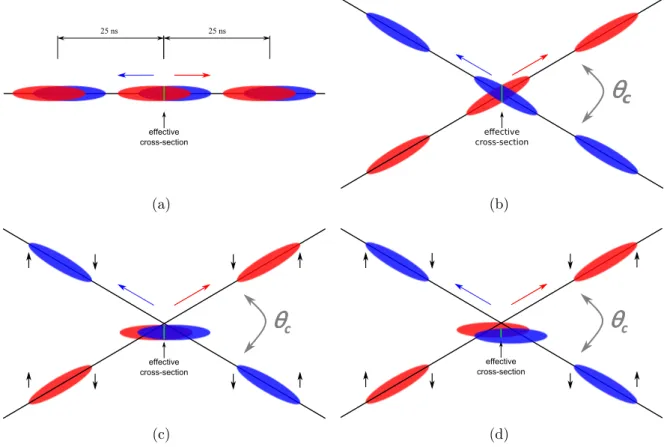
effective cross-section
25 ns 25 ns
(a)
θ θθ θ c
effective cross-section
(b)
θθθθ c
effective cross-section
(c)
θθθθ c
effective cross-section
(d)
Figure 1.2: Illustrations of bunch collision schemes at the IP. (a) illustrates the head-on collision case, (b) the case with a small crossing angle θ c . The HL-LHC scenarios using crab cavities are illustrated in (c) without and (d) with luminosity levelling.
Since the bunches are only separated by 25 ns multiple interactions would occur at different
positions in the detector, see Figure 1.2(a). Thus, the beams are collided with a small crossing
angle θ c , see Figure 1.2(b), and the geometric luminosity reduction factor at the IP F has to be
1.2 From LHC to HL-LHC 5
taken into account. Assuming that β ∗ is greater or equal than the Root Mean Square (RMS) of the bunch lenght σ z it is defined as:
F = 1
q
1 + θ 2σ c σ ∗ z
2 (1.3)
with σ ∗ denoting the transverse RMS beam size at the IP. The total peak luminosity is then given by
L peak = LF (1.4)
Table 1.1 gives an overview of the typical current and nominal design values for the beam parameters of the LHC.
Table 1.1: Current average (Oct. 2012) and nominal design beam parameters of the LHC in proton operation mode. The current values are always given at the IP of the ATLAS experiment. Additional the current planing for HL-LHC is given. For the pile-up estimation the inelastic p-p cross-section is used [47].
Parameter Name Symbol Current Design HL-LHC
[Unit] [48, 49] [43] [50]
Bunch Spacing [ns] 50 25 25 50
Number of bunches n b 1374 2808 2808 1404
Number of particles/bunch N b [10 11 ] 1.6 1.15 2.0 3.3 Revolution frequency f rev [kHz] 11.245 11.245 11.245 11.245
Normalised emittance n [µm] 2.4 3.75 2.5 3
Beta function at the IP β ∗ [m] 0.6 0.55 0.15 0.15
Crossing angle θ c [µrad] 290 300 420 520
RMS bunch length σ z [cm] ≥ 9 7.55 7.55 7.55
RMS beam size at the IP σ ∗ [µm] 19 16.7 13.6 10.0
L levelling factor 1 1 2.5 5
Pile-up hµi 19.5 19 140 140
Peak Luminostity L peak [10 34 cm −2 s −1 ] 0.7 1.0 5.3 7.6
Energy √
s [TeV] 8 14 14 14
1.2.3 Current Performance
In March 2010 the first physics run at an energy of 3.5 TeV per beam was started at the LHC
and the machine delivered 5.6 fb −1 until the end of 2011, while steadily increasing the peak
luminosity. During the winter shutdown the beam energy was slightly increased to 4 TeV and
23.3 fb −1 have been delivered in 2012. The delivered and the recorded luminosity for the years
2010–2012 are summarised in Figure 1.3 for the ATLAS experiment. Following a steep learning
curve the LHC is operated meanwhile with many parameters close to its nominal values, see
Table 1.1. For some parameters as N b and n , it even exceeds the nominal specifications. One
critical point is the beam energy, which cannot be raised further until the interconnections of the
dipole magnets are improved. Their in part too high resistance when compared to specifications
lead to a technical failure in 2008, delaying the start of the LHC by almost two years. Another
key area for further improvement will be the reduction of the bunch spacing from 50 ns to 25 ns
6 Upgrade Plans for the Large Hadron Collider and the ATLAS Detector
since this allows to reduce the number of simultaneous hard interactions per bunch crossing, the so-called pile-up µ, while increasing the peak luminosity and thus helps to reduce systematic uncertainties in the high energy physics measurements conducted by the collaborations.
(a) (b)
(c)
Figure 1.3: Evolution of the delivered and recorded integrated luminosity delivered for the ATLAS experiment in (a) 2010, (b) 2011, and (c) 2012 [49].
1.2.4 Upgrade Roadmap
To make the rare channels discussed above accessible, upgrading the LHC is planned in three steps, each coinciding with a Long Shutdown (LS) of the machine lasting between one and two years. Each shutdown has a slightly different focus.
LS1 – Consolidation
LS1 is dedicated to the consolidation of the LHC needed to reach the nominal performance in energy as well as in luminosity. Starting from early 2013 until the end of 2014 the connections between the magnets will be improved to allow for a higher current flow within the magnets leading to stronger magnetic fields, which are mandatory for LHC operation at √
s = 14 TeV.
The higher beam energy additionally allows for a further decreased β ∗ , such that in combination
with the higher energy a fourfold increase with respect to the present luminosity is expected
1.3 ATLAS 7
after the LS1 [2]. Given the present excellent performance of the LHC it is expected that the nominal peak luminosity will be exceeded already after LS1.
LS2 – LINAC 4
In the second LS, planned for the year 2018, a newly build LINAC [51] will be connected to the LHC accelerator complex as a replacement for the now used LINAC 2. This upgrade in combination with collimation upgrades in the accelerator complex allows for an increase of the number of particles per bunch, since the higher energy of 160 MeV of the protons after leaving the LINAC leads to a reduction of space charge induced losses in the transition from the LINAC into the Booster. The same effect is exploited in the next step, by increasing the final energy of the Booster to 2 GeV. Because of the quadratic contribution of N b to the luminosity (cf.
Equation 1.2) this leads to an estimated peak luminosity of L ≈ 2.5 · 10 34 cm −2 s −1 after the LS2 [2].
LS3 – HL-LHC
The target for the LS3—planned for 2021/2—is to increase the luminosity to (5–8) ·10 34 cm −2 s −1 and thus allowing for an integrated luminosity of 200–300 fb −1 /a. Several approaches are studied at the moment to achieve this luminosity increase. Besides, the obvious decreasing of the colliding area and filling the bunches with more particles, also the geometric luminosity reduction factor, Equation 1.3, at the IP will be optimised. One idea investigated, is the use of crab cavities [52,53], which effectively reduce the crossing angle θ c by rotating the bunches shortly before the collision as illustrated in Figure 1.2(c).
One important boundary condition is the number of pile-up events µ, since it is a challenging task to disentangle these events within the experiments. In the planning for the HL-LHC a hµi below 140 is envisaged. To reduce it and simultaneously increase the life-time of the beam, the bunches will be collided slightly off centred, such that the luminosity is levelled to a constant value over the fill, see Figure 1.2(d). Although, this decreases the instantaneous luminosity at the beginning of a run, the integrated recorded luminosity can be increased by this technique since the fill time of the machine is increased considerably.
The momentarily two most favoured parameter sets for HL-LHC operation are summarised in Table 1.1.
1.3 ATLAS
Aiming for the widest physics reach, ATLAS is built hermetical to cover almost 4π solid angle and to measure as many different physics signatures as possible. As other colliding beam experiments ATLAS has an onion shell layout, where each layer is specialised for a different purpose. Figure 1.4(a) gives an overview of the ATLAS experiment. Its structure and detection principles will be shortly summarised in the following. As the focus of this thesis is on the pixel detector, in Section 1.3.1 a more detailed description of this detector component is given. For the other sub-detectors the reader can find further details in the given references.
The detector parts can mostly be grouped in four functional groups: tracking, calorimetry,
magnets, and data acquisition. The tracking system is composed of the inner detector [56, 57],
which is embedded into a 2 T solenoid [58, 59] magnet and the muon system [60], which is
8 Upgrade Plans for the Large Hadron Collider and the ATLAS Detector
(a)
(b)
Figure 1.4: Illustrations of (a) the ATLAS detector [54] and (b) the components of its inner
detector [55].
1.3 ATLAS 9
embedded into a 4 T toroid magnet [58, 61, 62]. Exploiting the Lorentz force, the magnets, allow for a momentum determination of the charged particles measured in these detector parts.
The inner detector, see Figure 1.4(b), is composed by three sub-detector systems. The centre-most pixel detector and the surrounding SemiConductor Tracker (SCT) are based on segmented silicon sensors. While in the case of the SCT these segments are called strips, being several centimetres long with a pitch between 57 µm and 94 µm, for the pixel detector they are called pixels and their pitch is 50 µm × 400 µm. The Transition Radiation Tracker (TRT) employs straw-tubes filled with ioniziable gas and an anode wire in the centre. These tubes are interluded with fibres (barrel) and foils (end-caps) which evoke transition radiation and thus allow for discrimination of electrons and pions.
The muon system sheaths the detector and exploits four different technologies: the Monitored Drift Tubes (MDTs), the Cathode Strip Chambers (CSCs), the Thin Gap Chambers (TGCs), and the Resistive Plate Chambers (RPCs). While the first three detectors are devoted to tracking purposes, the last two ones are used for triggering. The detection principle of the MDTs which comprise for the majority of the muon system relies on straw-tubes filled with ioniziable gas and an anode wire in the centre. In high rate regions, i. e. in the pseudorapidity 5 range |η| ≥ 2, CSCs, which are Multi-Wire-Proportional Chambers (MWPCs) [63], are used.
The TGCs, also MWPCs, but with a larger anode-anode distance than anode-cathode distance, are used for tracking as well as triggering in the forward part. Finally the RPCs are used solely for triggering within the muon system and are built from parallel plates separated by a gaseous volume.
The calorimetry system [64], situated between the inner detector and the muon system, consists of two major parts: the electromagnetic [65] and the hadronic calorimeter [66]. The former one is accordion shaped with lead as absorber and liquid argon as active medium. It stops photons, electrons and low energetic, charged hadrons, while allowing for their energy determination; the hadronic calorimeter is optimised to stop hadrons by using materials with a large hadronic attenuation length. It uses scintillating polystyrene [67] tiles and iron absorbers in the barrel part; liquid argon with copper and tungsten absorbers are used in the endcap region.
A multi-level trigger system [68] ensures that out of the 40 million interactions per second the right ones can be selected and recorded with a manageable rate, of the order of 300 Hz.
1.3.1 The ATLAS Pixel Detector
The ATLAS pixel detector [69,70] is composed of three concentric barrel layers and two end-caps on both sides with three disks each. This geometry, formed by 1744 assemblies is optimised to ensure three hits in the pixel detector up to |η| = 2.5. The B-layer, which is located at a radius of 5.05 cm, is closest to the interaction point. In Figure 1.5 the structure of an assembly is illustrated. The active part is an n-in-n pixelated silicon sensor of 250 µm thickness and an area of 16.4 × 60.8 mm 2 yielding a position resolution of 10 µm in Rϕ and 110 µm in z. This sensor is connected via solder bump technology to 16 FE-I3 [71] read-out chips, with 2880 read-out channels each, adding up to more than 80 million read-out channels over the whole
5 The ATLAS coordinate frame is spanned by x, y, and z. The point (0,0,0) is located in the centre of the
detector. The x axis points to the centre of the ring and the y axis upwards; righthandedness defines the z
axis, which goes along the beam pipe. Alternatively the notation with the azimuth angle ϕ and the polar
angle ϑ is used. The angle ϕ = 0 points to the centre of the ring and ϑ = 0 points towards positive z. The
pseudorapidity η is defined by η := −ln tan(ϑ/2).
10 Upgrade Plans for the Large Hadron Collider and the ATLAS Detector
pixel detector. The 16 read-out chips on an assembly are connected via the flex—a flexible printed circuit board—to the Module Control Chip (MCC) [72], which coordinates, configures, triggers and reads-out the individual FE-I3 read-out chips. The data are then passed through the pig-tail onto the central read-out architecture. Evaporative C 3 F 8 -cooling is used to ensure that the pixel detector can always be cooled down to and be operated at −13 ◦ C.
Figure 1.5: Composition of an ATLAS pixel assembly [73].
1.3.2 Upgrade Roadmap
Alongside with the upgrade of the LHC the ATLAS detector will be upgraded in three phases to cope with the increased luminosity rates, which manifest themselves from the detector point of view in high radiation, trigger, and pile-up levels. Additionally, in all upgrade phases the repair and consolidation of detector parts, which where found to be failing during the preceding operational years is foreseen.
Phase 0
During the LS1 a new innermost pixel layer, the Insertable B-Layer (IBL) [74] will be installed
at a radius of 3.2 cm between the existing pixel detector and a new beam-pipe. Two sensor
technologies are planned to be used for the IBL detectors: silicon 3D [75] and n-in-n silicon
planar sensors. Additionally, a new read-out chip FE-I4 [76], which features smaller pitch sizes
of 250 µm × 50 µm and an approximately six times larger area than the present ATLAS read-out
chip FE-I3 [71] was developed for the IBL. The finer granularity of the pixels, leading to an
improved vertex-resolution, is crucial to disentangle the individual vertices in the high pile-up
regime after the consolidation phase of the LHC and improves the overall tracking performance.
1.3 ATLAS 11
Because of the small radius and the constrained space it is not possible to arrange the pixel modules with an overlap in z as it is done in the present pixel detector. Thus in the design for the sensors emphasis was put on the maximization of the active fraction.
Phase I
In the second upgrade phase, the aim is to preserve the nominal luminosity trigger acceptance after the LS1 upgrade and to prepare the detector for the LS2 upgrades. The Letter-Of- Intent (LOI) [77] was finished at the end of 2011 and focuses especially on upgrades to the forward regions (|η| ≥ 2.5) of the muon and calorimetry systems, where high occupancies are expected after the LHC upgrade. For the muon system this will be achieved by a small wheel in the forward region equipped with the MICROMEGAS [77, 78] detectors. These micro- pattern gas detectors provide tracking and trigger information. For the calorimetry system the investigations are still ongoing if the forward parts have to be replaced completely already at this point in time or if minor upgrades are able to allow for operation until phase II.
Phase II
In the last currently foreseen upgrade phase, corresponding to the LS3 of the LHC, the focus will be on the inner detector, which by then will be deteriorated by radiation to its design limits and likely require a complete replacement. Additionally, the increased track density will make an improved resolution mandatory at this point in time. A replacement completely based on silicon sensors is planned, and different layouts are under investigation at the moment. The currently planned baseline layout [79] is shown in Figure 1.6. It incorporates four pixel, three short strip (striplet), and two strip layers in the barrel part and six pixel as well as seven strip discs in the forward region. Depending on the physics performance found in future simulations it is planned to readjust the exact numbers of layers for the different technologies, e. g. by adding a fifth pixel layer instead of a striplet layer. In all cases a total of at least 14 hits is envisaged for each particle.
Due to the large total area of at least 7 m 2 foreseen for the future pixel detector, a cost reduction is required for all different components and steps of the assembly procedure, i. e.
starting from the sensor over the interconnection to the read-out chip. Additionally, in this harsh radiation environment the innermost layers will have to sustain very high integrated fluences of more than 10 16 n eq /cm 2 (1 MeV equiv.) [79]. The performance of differently produced silicon sensors at these extreme levels are explored at the moment by the experiments and within the RD 50 collaboration [80]. Especially, the inner layers have to resolve unprecedented track densities, which are foreseen to be addressed by reducing the pitch for the assemblies in these layers to 25 µm in Rϕ. This makes an improvement of the currently used solder bump interconnection technology, or the development of a new one, mandatory, since at the moment only pitches down to 50 µm are possible on a large scale. As for IBL, the innermost layer will be mounted as close as possible to the interaction point impeding overlapping assemblies. This reflects in the requirement of a maximised active fraction of the assembly. Finally, the material budget should be minimised as far as possible, to reduce multiple scattering. Although, the contribution to the material budget by the sensors and read-out chips is small 6 compared to the services, the use of thin sensors and read-out chips is envisaged, since their subsequent lower power consumption also reduces the amount of needed services considerably.
6 The radiation length of silicon is X 0 = 21.8234 g/cm 2 ≡ 9.366 cm [81, 82].
12 Upgrade Plans for the Large Hadron Collider and the ATLAS Detector
0.0 0.5 1.0 1.5 2.0 2.5 3.0 3.5
0.0 0.5 1.0 1.5
z (m)
r(m)
eta = 0.0 eta = 1.0
eta = 2.0
eta = 3.0
Figure 1.6: Baseline layout of the new inner detector foreseen in the LOI for the Phase II upgrade [79]. Pixel layers are indicates in red, strip and striplet layers are indicated in blue.
In addition to the upgrade of the inner detector, the calorimeter and the muon system will be upgraded mostly in terms of read-out electronics, which are believed to be not radiation hard enough, but also in some of the parts encountering high radiation levels after the upgrade.
1.4 The MPP/MPI-HLL Pixel Assembly Concept
In this thesis an assembly concept designed to answer the challenges of the ATLAS phase II upgrade is investigated. For comparison the current and the investigated pixel assembly concept is illustrated in Figure 1.7. The assembly concept builds upon five novel technologies in the field of pixel detectors and an optimised sensor design. n-in-p pixel sensors are thinned using a process developed at the Max-Planck-Institut HalbLeiterLabor (MPI-HLL) [83] and are connected to the read-out chip via the Solid Liquid Inter-Diffusion (SLID) technology of the Einrichtung f¨ ur Modulare Festk¨ orper-Technologien (EMFT). Signals are then routed via Inter-Chip-Vias (ICVs) through the read-out chip to the subsequent data acquisition chain. In addition, a newly designed edge area of the sensors is introduced to increase the active area of the detector or prospectively decrease the size of the inactive edge d inactive .
The main arguments in favour of this design and the challenges of these technologies will be
given shortly in the following subsections. In the subsequent chapters they will be investigated
in depth. This discussion is preceded by an introduction into semiconductor physics, up to the
level needed for an understanding of the following investigations in Chapter 2.
1.4 The MPP/MPI-HLL Pixel Assembly Concept 13
n-substrate
Read-out chip
Sensor
n
+HV Guard-rings
195 µm 250 µm Bump-balls
inactive
d
(a)
Thin read-out chip Thin sensor/active edge n
+
HV
IC V
60 µm 75 µm – 200 µm
inactive
d
BR(b)
Figure 1.7: (a) Schematics of the current pixel detector assembly structure within the ATLAS experiment and (b) the proposed design. The read-out chip is shown in blue, the sensor in light green (violet) for the current (new) concept. The pixel implants as well as the bias ring n + -implants are indicated in green, where the implant closest to the edge is the bias ring implant. The back-side and in the new concept case also the edge implantation is indicated in red. Wire bond pads are drawn in light blue, ICVs in yellow. (a) is adapted from and (b) inspired by [84].
1.4.1 n-in-p Sensors
In this assembly concept the n-type silicon substrate used in the current detectors is replaced by a p-type silicon substrate. This approach allows to place the electric field shaping implants, the so-called guard rings, on the same side as the pixel implantations. Consequently, only one side needs expensive patterned processing, resulting in a cost reduction by the sensor fabrication.
Up to now n-in-p pixel detectors were not employed in high energy physics experiments due to the prior unavailability of detector grade, high resistivity material and concerns on destructive discharges, due to the close distance between the sensor at high voltage and the read-out chip operated at ground potential. These novel devices were built for the first time in course of this thesis and their overall performance and in special their radiation hardness will be discussed and compared to the currently used n-in-n technology in Chapter 4. Following these investigations the ATLAS collaboration is currently planing to use n-in-p pixel sensors also for the outer layers of the phase II upgrade [79].
1.4.2 Thin Sensors
Exploiting thinner sensors reduces on the one hand the material budget and therefore multiple scattering. On the other hand they have higher electric fields than thicker devices, when the same bias voltage is applied. Thus they exhibit a higher signal collection efficiency after the high radiation doses expected in the environment of the HL-LHC, when employing a read-out electronics capable of working with reduced signal sizes. Since the smaller signal sizes need less read-out time in the ATLAS read-out chips, a lower signal also leads to a lower occupancy of the pixel detector. In addition, the lower needed operation voltages lead to a drastically reduced energy dissipation and lowers the noise levels especially after irradiation. Finally, preliminary simulations are suggesting that the vertex resolution is improved for tracking algorithms, when employing thin sensors, since the reduced diffusion confines the signal to a smaller region in space. Thin pixel sensors with d active = 75 µm and d active = 150 µm were built and investigated together with thin strip sensors of the same thickness. The results are presented in Chapter 5.
After encouraging results obtained in the prototyping runs, 200 µm thick sensors will be used for
the IBL-upgrade [74, 85]; for the phase II upgrade 150 µm or thinner sensors are envisaged [79].
14 Upgrade Plans for the Large Hadron Collider and the ATLAS Detector
1.4.3 3D-Integration
A rather new concept in the field of semiconductor based electronics is 3D-integration [86, 87].
Here several layers of electronics are stacked vertically and are interconnected through the volume of the chip, i. e. its 3 rd dimension. As a consequence the lines connecting different logic blocks of the chip become shorter resulting in possibly lower latencies, and lower line capacitances. This leads to a decrease of the noise and lowers the power consumption. When the functional blocks of the chips are distributed over different layers, also the area required to host them is reduced, allowing either for more sophisticated logic blocks in the same area or a decrease of the pixel cell size in the case of pixel detectors.
Furthermore, the different chip layers can either be done within the same processing technolo- gies or with different processes, for example optimised separately for the analogue and digital section of the chip, and then vertically interconnected. In the latter case an interconnection technology is needed that allows for consecutive interconnection of layers without breaking the connections of already connected layers. In this thesis the SLID interconnections, developed by the EMFT [88] is employed, which fulfils this criterion. For the vertical signal transport ICVs are envisaged.
SLID Interconnection
The SLID interconnection, developed by the EMFT [88], is a possible alternative to the currently used solder bump-bonding. After formation of the interconnection at around 300 ◦ C, it has a melting point around 600 ◦ C, and thus fulfils the requirement discussed above. The interconnection pitch can eventually be reduced down to approximately 20 µm [89], which is sufficient for the planned ATLAS phase II upgrades. Additionally, these interconnections can have arbitrary and different geometries. Furthermore, when compared to the currently used solder bump-bonding less process steps are needed, and thus an eventually lower cost is expected.
Inter-Chip Vias
In the assembly concept investigated here ICVs are used to transfer the signal to the back-side of the chip for read-out. By this the active area of the assembly can be increased considerably since the overhanging part of the read-out chip over the sensor, where traditionally the wire bonding pads are placed, can be shortened significantly. Together with the optimised edge region design d inactive is almost completely removed. During the ICV process the read-out chip is thinned to about 60 µm, which leads to a further reduction of the assembly thickness and thus of multiple scattering. After establishing the process and using a adequate read-out chip, the high aspect ratio vias 7 as they are investigated in this thesis could be transferred to a per pixel level. In this scenario two specialised chips—one for analogue and one for digital processing—could be stacked and the remaining overhang could be abolished completely.
1.4.4 Slim and Active Edges
In the present ATLAS pixel design the distance between the last pixel implant and the sensor edge is about 1.1 mm [70]. Additionally, the overhang of the read-out chip contributes about 2 mm to d inactive on one side. This area is insensitive to traversing particles. In the proposed
7 The aspect ratio is defined by the width of the via divided by its length.
1.4 The MPP/MPI-HLL Pixel Assembly Concept 15
assembly design d inactive is reduced considerably in two ways. First, the ICVs discussed in the preceding paragraph eventually allow to completely remove the balcony. Second, an improved guard ring design and an edge implantation reduces the distance between the last pixel implant and the sensor edge by a factor of 20.
1.4.5 Intermediate Designs for the R&D Process
To disentangle different effects and to study the implications of the individual new technologies presented in the previous sections, these were studied first in an independent way and then integrated into the same module. First the novel p-type bulk material was investigated using the presently used structure of the ATLAS pixel assembly. Additionally, here different variations of the edge designs were studied to increase the active fraction of the assembly. These results will be discussed in Chapter 4. Thin sensors were studied in a two-fold approach: first, as strip sensors, which due to their easier read-out result in shorter R&D cycles, second, as pixel detectors connected via conventional solder bump bonding and SLID inter-connection. The results of thin sensors are presented in Chapter 5. Additionally, a production of thin sensors incorporating active edges was conducted, and first results are reported in Chapter 5 as well.
Aiming for a demonstrator assembly incorporating four of the five new technologies—i. e.
n-in-p bulk material, thin sensors, SLID, and ICV—a two step approach was chosen. In the first step the first three technologies are included, while in the second step also ICVs are employed.
Both concepts are illustrated in Figure 1.8.
p-substrate
FE-I2 readout chip
sensor
n+
HV
option A option B
digital readout pad
Figure 1.8: Design of the assembly used for the R&D phase of the SLID and ICV technology [84].
In contrast to the currently used ATLAS assemblies both concepts rely on SLID pads instead
of solder bump-bonds to connect the sensors pixel cells to the read-out pixel cells. Since the
currently used ATLAS read-out chips are employed in this demonstrator assembly, additional
SLID pads are placed below the balcony to guarantee mechanical stability. The read-out of the
chip is handled differently in both variants. In the first variant, which will be treated in Chapter 6,
the wire bonding pads are connected via SLID pads to a fan-out structure incorporated into
the sensor design. In the second variant, the signals are routed to the back-side of the chip
employing ICVs. This variant will be discussed in Section 6.2.
2 Theory of Radiation Hard Pixel Detectors
In high energy physics experiments, semiconductor based detectors have been replacing gas based detectors in the tracking systems, since they offer a much better position information and an improved energy resolution. Today all experiments, which require high spatial resolution for tracking, employ semiconductor based detectors.
Pixel detectors are segmented semiconductor devices with an area smaller than 1 mm 2 per segment and more than 10 3 segments [90]. The individual segments are called pixels. Given the high cell multiplicity, signals cannot be routed easily from the centre to the edges of the devices and so every pixel cell is individually connected to the corresponding read-out channel of the read-out chip. This approach is commonly called hybrid pixel detector, while special realisations are generally referred to as module or assembly.
Within the read-out chip of a hybrid pixel detector some logic blocks, like the communication interface to the subsequent read-out chain, cannot be distributed to the individual pixel cells because of space constraints. Thus, a region without active counterpart on the sensor side at one side of the chip is needed for connection to the subsequent read-out, leading to a blind spot of the assembly. An alternative approach would be to route the signals to the other side of the read-out chip by etching ICVs through the chip and placing the read-out logics on the back-side.
In the following chapter an introduction to pixel sensors is given with a focus on effects relevant for the investigations presented in this thesis. The chapter is not aiming for a complete introduction to semiconductor physics, which can be found for example in [90–92], and thus many details are omitted.
2.1 Physical Foundations
While electrons in free atoms are confined to discrete energy levels, these levels merge and become bands if atoms are brought to distances typical of the crystal reticule. Depending on the specific element forming the crystal at a temperature T of 0 K, the highest energetic populated band, the valence band, is either fully or partially filled. In the latter case the material is a conductor since the electrons move freely through the crystal within the not filled phase space region. If the valence band is fully filled the material becomes an insulator or semiconductor.
The transition between the two states is smooth and is mainly defined by the energy difference between the highest possible energy in the valence band E V to the lowest energy of the next free band E C , called conduction band. This energy difference is also called band gap E g .
If the band gap is small enough, electrons from the valence band can be thermally excited to the conduction band. The probability that a specific phase space state in the band structure is occupied by a charge carrier is described by the Fermi-Dirac-function
f e (E) = 1
1 + e (E−E f )/kT (2.1)
18 Theory of Radiation Hard Pixel Detectors
with k the Boltzmann constant and E f the Fermi energy. E f is defined via the macroscopic neutrality of the crystal and thus:
E f = E C − E V
2 + O(0.01 eV) ≈ E g
2 (2.2)
which corresponds to the middle of the band gap.
Silicon is the most commonly used semiconductor material thanks to its wide availability, its low price and the high technological level reached in its processing. It is an element semiconductor which crystallizes in the diamond structure and has a minimal band gap of E g (300 K) = 1.12 eV.
2.1.1 Intrinsic and Extrinsic Semiconductors
If the crystal is intrinsic, i. e. without or with a negligible amount of impurities, the charge carrier concentrations, measuring the occupied phase space states which can move freely through the crystal, for electrons n e and positive states—also called holes—n p are in an equilibrium state and equal the so-called intrinsic charge carrier concentration n i . For silicon this is n i (300 K) = (1.09 ± 0.09) · 10 10 cm −3 [93]. This is typically below minimum concentration of impurities that can be achieved in the semiconductor industry, lying at 10 12 cm −3 .
To define and control the properties of the silicon, additional dopants are used, which means certain impurities are introduced artificially to enhance either n e or n p . The most commonly used dopants are atoms from the III (e. g. boron) or the V (e. g. phosphorus) main group of the periodic system of the elements. The former type of dopants leads to additional holes in the crystal since these atoms are not able to form bonds with all their neighbours. In the band scheme this corresponds to the introduction of an additional acceptor level E A at (20–60) meV above the valence band (Figure 2.1(a) left) depending on the element used [91]. Silicon doped in this way is called p-type silicon. If instead atoms of the V main group are used for the doping, additional electrons are introduced since they are superfluous to form the bonds in the crystal.
In the band scheme this is represented as a new donor level E D at (40–50) meV below the conduction band (Figure 2.1(a) right) depending on the element used [91]. This type of silicon is called n-type silicon. In both cases the newly introduced levels are so close to either the valence or the conduction band that thermal excitation leads to an almost complete excitation of the newly introduced states resulting in a shift of the Fermi energy towards the respective newly introduced level. Hence, electrons are the majority charge carriers in the n-type material (n e n p ) and holes respectively in p-type material (n p n e ).
2.1.2 The pn-Junction
The basic principle of a pixel sensor is a pn-junction which is reversely biased and thus leads to an electric field able to collect the charge. A pn-junction is created by bringing together p-type silicon with n-type silicon as shown in Figure 2.1(b).
In the transition zone from n- to p-type the free electrons from the n-type will diffuse to the p-type part and neutralize free holes, which themselves will diffuse into the n-type part and neutralize free electrons. Since the movable charge carriers are neutralised only the fixed charges stay, namely the ionised donors in the n-type part and the ionised acceptors in the p-type part.
In sum this leads to a region with a non vanishing charge ρ, the space charge region. The
2.1 Physical Foundations 19
p
n E E C,p
E V,p
E A
E f,p
E C,n
E V,n
E D
E f,n
(a)
p
n
E C,p
E V,p
E A
E C,n
E V,n
E D
E
E f,p
E f,n
eV bi
(b)
Figure 2.1: Schematics of a pn-junction. (a) Illustrates on the left (right) the different energy levels in p-type (n-type) silicon. In (b) the configuration after bringing the differently doped regions together is drawn. Four different energy levels E are indicated for each type by an index, where C (V) denotes the lowest (highest) level in the conduction (valence) band, A (D) the acceptor (donator) levels and f the Fermi energy. Additionally, states in p-type and n-type silicon are differentiated by the index p and n.
resulting potential φ prevents further diffusion of charge carriers and can be calculated via the Poisson equation:
− ∇ 2 φ = ρ(x)
0 (2.3)
Outside of the space charge region, ρ(x) vanishes, since the mobile charge carriers neutralise the acceptors and donors. The maximal potential difference φ is called built-in voltage V bi , which is of O(1 V), see Figure 2.1(b). If an external voltage is applied to the pn-junction it can be either of opposite or same polarity as V bi . The former scenario is referred to as forward bias, the second as reverse bias. Since the latter is the standard operation setting for pixel detectors, in the following reverse bias will be defined as positive.
In forward bias, charge carriers are forced back into the depleted zone, which eventually becomes a conducting zone. This leads to an exponentially rising current. On the contrary reverse bias further removes free charge carriers from the not yet depleted regions and thus enlarges this region. The width of the depleted zone W is proportional to
p V + V bi ≈ √
V (2.4)
where V is the applied bias voltage. Since charge creation takes place predominantly in the depleted region, its width before irradiation is proportional to the obtainable signal height.
The voltage for which the width of the depleted zone equals the thickness of the detector d is
called full depletion voltage V fd . A pn-junction operated at even higher voltages is said to be
over-depleted and the electric field is incremented by a constant field of (V − V fd )/d.
20 Theory of Radiation Hard Pixel Detectors
2.1.3 Charge Generation
The two most important effects of charge carrier generation in pixel detectors in stable operation are the mentioned thermal excitation and the generation by charged particles.
The signal generation by heavy charged particles originates from many scattering interactions of the particles with the electron clouds of the crystal lattice leading to an energy transfer.
The average energy transfer per traversed length of material is described by the Bethe-Bloch- function [94, 95]. Dividing the resulting energy by the average energy needed to create an electron hole pair in silicon, of 3.6 eV/e [96] leads to the average signal height which can be expected from a device. This average value is higher than the Most Probable Value (MPV) ∆ p since the former also accounts for large energy deposits resulting from knock-on- and δ-electrons 1 . The whole spectrum is described by a Landau-distribution shown exemplary in Figure 2.2(a) for different sensor thicknesses. As shown, the effect of knock-on and δ-electrons gets smaller for thinner detectors since they are not fully stopped within the sensor volume. In Figure 2.2(b) the MPV of the charge corresponding to the generated electron-hole pairs is drawn as a function of the sensor thickness for different impinging particle types and energies and momenta respectively.
The curves are calculated using the equations given in [97, 98] and the values of the occurring physical constants and material parameters from [82, 96, 97]. Particle types used in this thesis
100 200 300 400 500 600
0.0 0.2 0.4 0.6 0.8 1.0
f(∆/ x)
∆/x (eV/µm )
∆ p /x
Mean energy loss rate 500 MeV pion in silicon
640 µm (149 mg/cm
2) 320 µm (74.7 mg/cm
2) 160 µm (37.4 mg/cm
2) 80 µm (18.7 mg/cm
2)
(a)
µ m]
Thickness [ 50 100 150 200 250 300 350 400
m] µ MPV [e/
60 65 70 75 80 85
500 MeV pion 120 GeV pion 6 GeV electron
90
![Figure 1.1: The LHC accelerator complex and its embedding into the CERN accelerators [44].](https://thumb-eu.123doks.com/thumbv2/1library_info/4024614.1542018/17.892.120.786.304.815/figure-lhc-accelerator-complex-embedding-cern-accelerators.webp)
![Figure 1.3: Evolution of the delivered and recorded integrated luminosity delivered for the ATLAS experiment in (a) 2010, (b) 2011, and (c) 2012 [49].](https://thumb-eu.123doks.com/thumbv2/1library_info/4024614.1542018/20.892.135.725.213.714/figure-evolution-delivered-recorded-integrated-luminosity-delivered-experiment.webp)
![Figure 2.4: Evolution of V fd and |N eff | for an n-type sensor with the received NIEL-fluence [101].](https://thumb-eu.123doks.com/thumbv2/1library_info/4024614.1542018/37.892.247.664.151.425/figure-evolution-eff-type-sensor-received-niel-fluence.webp)
![Figure 3.9: Photographs, to scale, of the FE-I2/3 (left) and the FE-I4 (right) [85] read-out chips](https://thumb-eu.123doks.com/thumbv2/1library_info/4024614.1542018/54.892.105.770.163.490/figure-photographs-scale-fe-left-right-read-chips.webp)
![Figure 3.11: Photograph of the USBPix system components [139] with a Single Chip Card for FE-I3 assemblies.](https://thumb-eu.123doks.com/thumbv2/1library_info/4024614.1542018/56.892.104.770.489.894/figure-photograph-usbpix-components-single-chip-card-assemblies.webp)
