Silicon Tracking Detectors in High Energy Physics
Frank Hartmanna,∗
aInstitut f¨ur Experimentelle Kernphysik, KIT, Karlsruhe, Germany
Abstract
Since the 50ties semiconductors have been used as energy spectrometers mainly in unsegmented ways. With the planar technique of processing silicon sensors in unprecedented precession, strip like segmentation allowed precise tracking and even vertexing, culminating in the early 80ties within NA11 in the tagging of heavy flavour quarks – here thec-quark. With the following miniaturization of electronics, dense detector application haven been made possible and large scale systems were established in the heart of all LEP detectors, permitting vertexing in barrel like detectors. At the time of LEP and the TEVATRON tasks were still bifurcated, while small (up to 3 layers) silicon detectors did the vertexing and further out gaseous detectors (e.g. drift chambers or time projection chambers) with larger lever arms did the tracking. In run II of the CDF detector, larger silicon tracking devices, still complemented with a huge drift chamber, started to have a stand-alone tracking. At the LHC, ATLAS and CMS bifurcate in a slightly differen way, while silicon pixel detectors are responsible for the vertex- ting large volume silicon strip detectors (up to 14 layers) are the main tracking devices.
Silicon Tracking systems are a fundamental part of nowadays multipurpose high energy physics experiments. Despite the vertexing and thus heavy quark tag- ging, silicon tracking detectors in combination with a strong B-field deliver the most accurate momentum measurement and for a large range also the best en- ergy measurement.
In this chapter, the functionality of pixel and strip sensors will be introduced as well as a historic examples will be given to demonstrate the different imple- mentation highlights of the last 30 years.
Key words: silicon sensors, tracking detectors, radiation hardness, SLHC, RD50, ILC, vertexing
PACS:29.40.Wk, 29.40.Gx
∗Frank Hartmann
Email addresses: Frank.Hartmann@cern.ch(Frank Hartmann )
1. Principle
The concept will be introduced and the basic formulas will be listed without any real derivation. More basic and detailed discussions can be found in [1, 2, 3, 4, 5, 6]. Simple designs of sensors and modules is presented as well as their behaviour under radiation, which is, due to their close position to the interaction point, one of the major issues of design and research.
1.1. Basic Sensor Parameters
Silicon is a semiconductor; solid matter, which isolates at low temperatures and shows a measurable conductance at higher temperatures. The specific conductance of 102 to 10−9Ω−1cm−1 lies somewhere between metals and in- sulators. Silicon, the element which revolutionized the development of elec- tronics, is known as an important and multi-useable material, dominating to- day’s electronic technology. Silicon sensors have a very good intrinsic energy resolution: for every 3.6 eV released by a particle crossing the medium, one electron-hole pair is produced. Compared to about 30 eV required to ionize a gas molecule in a gaseous detector, one gets 10 times the number of parti- cles in silicon. The average energy loss and high ionized particle number with 390 eV /µm ∼ 108 (electron−hole pairs)/µm is effectively high due to the high density of silicon.
The usefulness and success of silicon can be explained in a handful of keywords:
• existence in abundance
• energy band gap
• possibility to change gap properties by defined adding of certain impurity atoms (dopants)
• the existence of a natural oxide.
• microscopic structuring by industrial lithography
By adding Type III and Type V atoms ”p-” and ”n-type” material can be formed which then in combination forms a ”pn-junction”. The surface of the sensor volumes of one type is then structured with the other type – the structures and the volume forms a multitude of pn-junctions. Structuring can be strip- or pixel-like. The possibility to deplete the full sensor volume of free charge carriers by applying a ”high” reverse bias voltage on the pn-junctions is one the keys of success. The natural oxide allows passivation of the sensor but can also be easily used as insulation oxide to allow in-sensor coupling capacitors.
For the reverse bias case, charge created in the space charge region SCR can be collected at the junction (strips or pixels), while charge created in the non- depleted zone recombines with free majority carriers and is lost. Operation conditions, namely voltage Vexternal is therefore such, that the full volume is
depleted. With Vexternal = Vbias larger than the diffusion or built-in voltage from the pure pn-junction,wresults to
w=p
2²%µVbias (1)
and vice versa
Vf ull depletion=VF D= D2
2²µ% (2)
withw=Das the full sensor thickness,µas mobility and%as bulk resistivity.
VF D is one of the most important design parameters, describing the minimal operation voltage, the sensor has to sustain without going into current break- down. In material dominated by one type of impurity, e.g the donor dopant densityNdis much larger than the intrinsic carrier concentration, the following expression for the resistivity%is valid:
ρ = 1
e(µNd) (3)
The mobility for electrons and holes areµe= 1350cm2/V sandµh= 450cm2/V s, resulting in about 10nsreadout time in around 100 µmthick silicon.
The second important operation parameter is the leakage current, defining power consumption, shot noise and also potential warm-up possibly resulting in ther- mal run-away. WithVbias > VF D, the equilibrium is disturbed and the estab- lished electrical field sweeps the thermally generated electron hole pairs in the SCR GSCR out of the depletion region. The emission process is dominated by the Shockley-Read-Hall transitions, resulting in a reverse current also called
”leakage current” IL being described by IL= 1
2eni
τLw·A (4)
with the surfaceAof the junction,wthickness (basically volume), the intrinsic carrier densityniand the generation lifetimeτL as a main parameter. In short, the leakage current is completely dominated by the effective lifetime τL (the generation lifetime of minority carriers), namely the impurity states Nt near mid-gap, e.g. Au and all novel metals are”lifetime killers”. The temperature dependency enters indirectly viani×T2∝e2kTEg.
The current increases linearly withw∝√
V until the detector is fully depleted.
At higher bias voltage an electrical breakdown is observed, where the current starts to increase dramatically. The breakdown can either be explained by
”avalanche breakdown”, due to charge multiplication in charge collisions with the lattice or by”Zener breakdown”, based on the quantum mechanical”tunnel effect”. Fig. 1 showsI∝√
V behaviour, as well as a breakdown.
To determine the depletion voltage, the capacitance to voltage dependency is exploited. The full capacitance of a sensor can be calculated by regarding the two planes of the SCR as plates capacitor with silicon as dielectric inside. C
decreases linear withwand therefore∼√ V: Cbulk=
( Aq
²Si
2%µVbias Vbias≤VF D
AD ²Si
depletion =const. Vbias> VF D
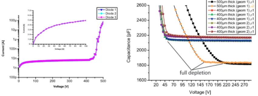
(5) Fig. 1 expresses the C and VF D dependency on area, thickness and %. The capacity-voltage characteristic CV or 1/C2versus voltages behaviour is used as a standard method to determineVF D. The kink determinesVF D.
0 100 200 300 400 500
100p 1n 10n 100n 1µ 10µ 100µ
0102030405060708090100 0.0
1.0n 2.0n 3.0n 4.0n 5.0n 6.0n 7.0n
Current [A]
Voltage [V]
Diode 1
Diode 2
Diode 3
Current [A]
Voltage [V]
full depletion
Figure 1: The current voltage characteristic for a Si-diode in the reverse bias direction is depicted. The expanded view shows theI∝√
V dependence, while the global view shows the full scan including breakdown at higher voltages.
The measurement plots describe the capacitance dependence on area and thickness quite clearly. The x-axis coordinate of the kink shows the depletion voltage, defined by mate- rial resistance and thickness. They-coordinate of the plateau shows the minimal capacitance, defined by area and thickness. The two upper bands depict sensors of two different geometries with slightly different areas and same high resistivity material, bothd= 400µmthick. The lower CV curves described= 500µmthick sensors. With increased thickness, C becomes smaller andVdepletion ∝D2 becomes larger. The different depletion voltages of the lower curves derive from two different resistivities%2> %1.
The last important basic parameter to be mentioned here is the electrical field resulting from the applied bias voltage. The field has its maximal strength at the main junction, e.g. the segmented face in an p-in-n sensor before irradiation withEM AX/M IN= V±VDF D at the faces. The sensor design (geometry andVF D) has to guarantee that the field is always below the break down voltage of silicon or with some tricks described later below the breakdown voltage ofSiO2
Besides these more bulk-like properties, also surface interfaces have to be mon- itored carefully to guarantee low parasitic and load capacities, also surface cur- rents must be kept low to guarantee segmentation isolation.
1.2. Silicon Strip & Pixel Sensors; Operation Principle
All tracking detectors make use of the free charges resulting from the ion- ization of a passing charged particle in a medium, e.g. gas or a semiconductor.
The average charge loss of a charged particle in a medium is described by the Bethe-Bloch formula.
−dE
dx = 4πNAr2emec2z2Z A
1 β2
·1 2ln
µ2mec2β2γ2Tmax
I2
−β2−δ(γ) 2
¸ (6)
In this formula z is the charge of the incident particle, Tmax the maximum kinetic energy which can be imparted to a free electron in a single collision,I the mean excitation energy,Z the atomic number, Athe atomic mass,NAthe Avogadro’s numbermethe electron mass, cspeed of light,reclassical electron radius,β=v/candγ=√ 1
1−β2 andδdensity effect correction. A more detailed description can be found in [7]. The most prominent part is the minimum at approximately βγ = 3, expressing the minimum of deposited energy in the medium. Every detector must be able to keep its noise well below this energy to be able to detect theseMinimum Ionizing Particles MIPs.
In addition, there are statistical fluctuations, a subject investigated in depth by Landau. The number of collisions in a finite medium as well as the energy transfer per scattering varies. The first effect can be described by a Poisson dis- tribution, while the later is described by a ”straggling function” first deduced by Landau. In rarer cases, called δ-rays orδ-electrons, the transferred energy is large, these δ-electrons are responsible for the asymmetric long tail towards high charge deposits. All in all the most probable value of energy transfer is about 30% lower than the average value. For silicon, the average energy used for the creation of one electron-hole pair in the indirect semiconductor is 3.6eV, about three times larger than the band gap of 1.12eV, deriving from the fact, that part of the deposited energy is used for phonon creation. For a MIP the most probable number of electron-hole pairs generated in 1µmof silicon is 76, while the average is 108.
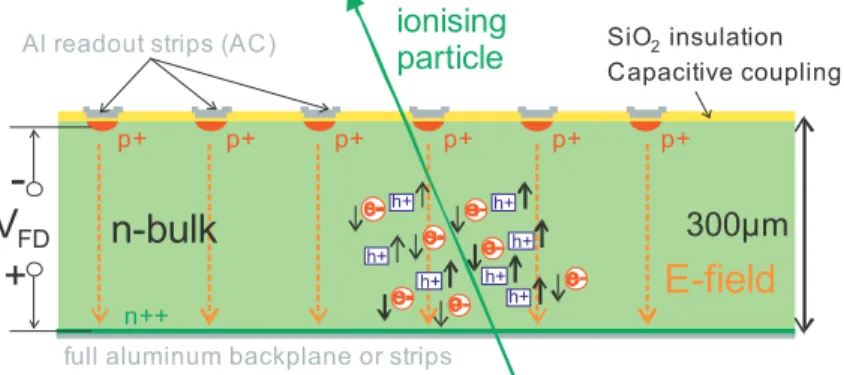
The working principle of a silicon micro strip detector is illustrated in Fig. 2.
An ionizing particle penetrates through a fully depleted siliconn doped slice.
n++
p+ p+ p+ p+ p+ p+
Al readout strips (AC)
full aluminum backplane or strips
ionising
particle SiO insulation Capacitive coupling
2
300µm
V
FD+
-
E-field n-bulk
h+ h+
h+ h+
h+
h+ h+
Figure 2:Working Principle of an AC-coupled Silicon Micro Strip Detector
Electron-hole pairs resulting from the ionization of the crossing charged particle, according the Bethe-Bloch-Formula, travel to the electrodes on the sensor planes. The segmentation in the pn-junctions allows to collect the charges on a small number of strips, where they capacitively couple to the Al readout strips. These are then connected to the readout electronics, where the intrinsic signal is shaped and amplified. In the case of segmented p strip implants in an n-bulk silicon material, holes are collected at the p strips.
The generated holes drift along the electrical field, created by the bias voltage,
to the p+ doped strips1 while the electrons drift to the n+ backplane. The charges collected on the doped strips are then induced, by capacitive coupling, to the aluminium readout strips, which are directly connected2 to the charge- preamplifier of the readout chip. In principle, the capacitor does not need to be implemented on the wafer, it can also be instrumented inside the readout chip or in between, this was for example the case for the NA11[18] experiment.
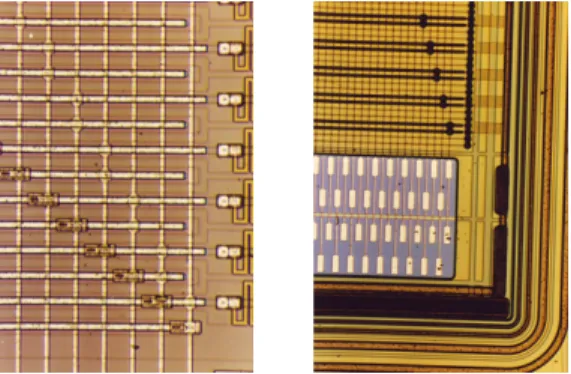
Sensors with integrated capacitors are called AC-coupled and otherwise DC- coupled. Because the capacitor needs to be large, the full strip length consists of ap+ oxide metal sandwich for example in the DELPHI (Section 2.2), CDF (Section 2.3) and CMS experiment (Section 2.4). TheSitoSiO2affinity allows an easy integration of a capacitive coupling of diode to metal contact, thereby allowing the use of a charge amplifying chip. A top view photo of a sensor with descriptions of the diverse sensor elements is presented in Fig. 3. Fig. 4 displays
Precison marker
Strip number
AC Pad
DC Pad
Bias resistor Rpoly
Biasring Guardring Outer protecting ring (for CMS: AL over n++)
SiO2coveringSi
Figure 3: The top view of a sensor, the ring structures, like n+ + active edge protecting ring, guard ring and bias ring are easy to spot. Both guard and bias ring are Al structures located on top of the p+ implants, they are directly contacted. Precision markers are needed to enable a precision assembly, while the strip numbers facilitate problem reports during quality assurance. The bias resistors connect thep+ strip located below the aluminium strips to the bias ring. A number of AC-pads are processed at the end of the strips to enable several connections to the readout electronics. The DC-pad, a direct contact to the p+ strip enables probing.
a three dimensional view of a standard single sided sensor design – the main elements are described in the caption. It should be mentioned that segmenta- tion of the bulk silicon material can be done on both sides with many benefits but also many additional problems. The obvious benefit is a 2-dimensional readout with different strip orientation on each side3 of a single sensor. Strip implants are then composed ofp+ andn+ on the two sides, named junction and ohmic side respectively. The ohmic side, withn+ + strips in ann-bulk needs special attention to arrange strip isolation due to the presence of an electron
1in ann-in-n,n-in-por a double sided detector, electrons drift to then+doped strips
2most often by ultrasonic wire-bonding
3Common strip orientations are 90o or a small stereo angle like 0.1 to 2o
n++ layer n-bulk
n++rin g
n++
ring
strip p+im
plants
passivation SiO oxide2
DC-pad AC-pad bias ring
guardring
bias resistor
coupling capacity oxide SiO2
vias
vias
Alstrips p+implants
aluminium backplane alignment
marker
passiva tion openin
gs
Figure 4: A 3D schematic is sketched. It shows the baseline of the CMS sensor at the LHC in 2008, but could represent basically any single sided AC-coupledRpolybiased sensor.
In operation, the bias ring is connected to GND potential, which is then distributed to the p+ implant strips, while the Al backplane is set to positive high voltage depleting the full n-bulk volume by forming apn-junctionp+strip ton-bulk. The coupling capacitor is defined between aluminium strip andp+implant; the inter-strip capacity between neighboring strips (bothp+and Al part). The guard ring shapes the field at the borders. Then+ +ring defines the volume and prevents high field in the real cut edge regions. [5]
accumulation layer with additionalp+ doping in betweenn+ strips or electron repelling field plates (same isolation criteria applies for n-strips in a p-bulk).
Fig. 5 presents the ultimate technology mix, a double sided sensor with inte- grated coupling capacitors, serving also as field plate on then-side, bias voltage supplied via polysilicon resistors and finally a double metal layer to allow per- pendicular strip routing. Figure 6 shows the top view of DELPHI double sided sensors.
The final position of the penetration is then calculated by analyzing the signal pulse height distribution on the affected strips. The strip pitch is a very important parameter in the design of the micro strip sensor. In gaseous detectors with a high charge multiplication a signal distribution over several sense wires are welcome to reconstruct the shape of the charge distribution and find the center. In silicon detectors there is no charge multiplication and small charges would be lost in the noise distribution. Therefore signal spreading over many strips could result in a loss of resolution. For single strip events the track position is given by the strip number. For tracks generating enough charge on two strips to exceed the threshold value, the position can be determined more precisely by either calculating the ”center of gravity”4 or by using an algorithm, that takes
4Assuming a uniform charge distribution, a track crossing between two strips at34×pitch will store 14×chargeon the left strip and 34×chargeon the right strip
bias ring; GND connecting to p+
bias ring; +V connecting to n+
polysilicon resistors aluminium routing strips (1µm)
p+ implants
n+ implants aluminium strip (1µm)
with metal overhang
silicon n-bulk
(300µm)
polyimide(5µm)
SiO (AC-coupling)2
(0.2 µm)
p+ stops metal-metal vias
Figure 5:The DELPHI Double Sided, Double Metal Sensor Scheme
The sensors contain novel integrated coupling capacitors, the bias is applied via high resistive polysilicon resistors, then-side strips are routed via a second metal routing layer and the innovative field plate configuration guarantees100MΩnstrip isolation. [5]
into account the actual shape of the charge distribution5 and the acceptance of the sensor. In short, the resolution with analog readout is given by
σx∝ pitch
signal/noise (7)
As a result, sensors with a pitch ofp = 25 µm and a signal/noise S/N of 50 have a position resolution of 2−4µm. Additional intermediate implant strips in between readout strips improve the resolution further by capacitively coupling to the readout strips. This technique helps to minimize number of electronic channels while achieving an adequate position resolution. For digital readout, the position resolution is given byσx≈p/√
126.
Another method to achieve a two-dimensional readout would be a pixelated segmentation. From the sensor point of view the design and processes are marginally different in the first approximation. The main difference if the con- nectivity to the electronics. While strips reach the end of the sensor, electronics can be wire-bonded while to each all pixels the readout covers the complete sen- sor are channels are ”bump-” or ”flip-chip”-bonded. A scheme can be seen in Fig. 7. The sandwich is often called Hybrid Active Pixel Sensor HAPS. HAPS are the main pixel species in the field of High Energy Physics, while in other area mostly Charged Coupled Devices CCDs or Monolithic Active Pixels MAPS (CMOS) sensors are in use but they are either to slow or not radiation hard for the collider environment.
5Approximately a Gaussian distribution, due to the diffusion profile
6σx≈p/√
12 arising from geometrical reflections: <∆x2>=1pRp/2
−p/2x2dx= p122
Figure 6: The left photo shows the microscopic view of then-side of a double sidedsensor.
The right picture shows a single sidedRzsensor.
The perpendicular strip arrangement with the contact vias can be seen on both pictures. Both sensors are using the double metal routing to connect the strips to the readout channels. The meander structures, the polysilicon resistors, connect the bias voltage to the implants. The polysilicon length and narrow shape defines the high resistance. On the left picture then-side structure, thep+stop structures surrounding every second implant are clearly visible. They are responsible for the strip to strip isolation. The sensor on the right is also interesting;
always two metal strips are connected together with two non-metallized intermediate strips (implants only) in between. With a50µm implant pitch, this gives200µm readout pitch with good charge sharing. The intermediate strips were connected to the bias ring via bias resistors on the other end of the sensor to guarantee a uniform potential on all implants. For the sensor on the left every single strip is connected to the readout. This gives a bit of an impression of the variety of sensors in the detector.
1.3. Irradiation damage
Tracking detectors are situated in the heart of the large HEP detectors, as close as possible to the particle interactions, suffering a harsh environment.
Traversing particles are not only ionizing the lattice but they also interact with the atomic bodies via the electromagnetic and strong forces. Atoms are dis- placed and create interstitials I, vacancies V and more complex constructs, e.g. di-vacanciesV2 or even triple-vacanciesV3, also di-interstitialsI2 are com- mon. All these defects deform the lattice. In addition diffusing Si atoms or vacancies often form combinations with impurity atoms, like oxygen, phospho- rus or carbon, again with different properties. Radiation fluence grows with increasing integrated luminosity and lower radius. It should be mentioned here that different particles do different damages, lower energy charged particles in- cite more point like defects, while higher energetic charged particles and also neutral particles (e.g. neutrons) do more cluster-like damage. For materials (n-bulk floatzone) used in current detectors damage of different particles can be normalized to ”1MeV neutron equivalent” damage by the so called Non Ioniz- ing Energy Loss NIEL hypothesis and mostly fluence numbers are given with this normalization. Thanks to dedicated R&D collaborations, e.g. RD48 and RD50[8], plus enormous effort inside HEP detector collaborations, the current understanding of radiation damage and its time evolution is quite sufficient to design current TEVATRON and LHC experiments and operate them for many
photoresist bumb material e.g. PbSn
pixel implant, e.g. n++
Si-bulk
bumb after reflow
pixel implant, e.g. n++
Si-bulk
metal pad
HAPS-sensor-cell HAPS-readout-cell
bump bond 200-300µm
standard CMOS low resistivity IC wafer readout chip
standard high resistivity depleted -coupled sensor
+ +
+ + - -
- -
CMOS wafer / readout chip
ionising particle pixel implant, e.g. n++
depleted Si-bulk a)
b)
c)
Figure 7:Scheme of aHybridActivePixelSensor HAPS
A HAPS is a sandwich of a silicon sensor and a standard CMOS readout chip. The sensor is of the high resistivity depleted DC-coupled type. The readout chip is realized in standard CMOS technology on a low resistivity wafer, the same size as the sensor and its readout cells are distributed in the same ”pixellated” way as the sensor pixels. The merging is realized via so called ”bump bonding” or ”flip-chip-bonding”. After preparing the pads with a dedicated under-bump-metallization a further lithography step opens holes on each pad to place the bump metal (a), e.g.CuorIn. After removing/etching the photoresist the metal undergoes another temperature step, the so called reflow to form balls of metal (b). The chip is then ”flipped”, aligned and pressed onto the sensor, warmed up for reflow, connecting sensor channels to readout cells (c).
years. The very basics of radiation damage are presented in [9] and [10, 11], recent studies on fully segmented sensors on a large sample can be found in [12] and [13]; a summary can be found in [5]. The three main effects (bulk and surface defects) introduced by radiation are
• displacement of atoms from their positions in the lattice (bulk)
• transient and long term ionisation in insulator layers (surface)
• formation of interface defects (surface)
This chapter will explain mainly the bulk defects, namely
• at 1014 n1M eV/cm2 the main problem is the increase of leakage current
• at 1015 n1M eV/cm2 the high resulting depletion voltage is problematic, increase ofNef f
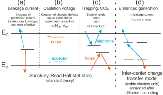
• at 1016 n1M eV/cm2 the fundamental problem is the CCE degradation Fig. 8 shows educationally the correspondence of deep energy levels in the band gap and their macroscopic electrical counterpart. The WODEAN and RD50 collaborations are systematically improving the qualitative understanding of microscopic defects and macroscopic degradation with respect to radiation of
different particles and annealing evolution. It should be mentioned that the levels shown in Fig. 8 can be introduced by irradiation bulk defects or by initial impurities.
+
-
donor
acceptor
EC
EV
Leakage current Increase of generation current Levels close to midgap
are most effective
Depletion voltage Trapping, CCE Creation of charged defects
upper band: donor lower band: acceptors
N ; Veff FD
⇒
Shockley-Read Hall statistics (standard theory)
Inter-center charge transfer model (inside clusters only)
enhanced after diffusion - annealing Enhanced generation
⇒
⇒ leakage current space charge
electrons
holes Shallow levels
trap e trap h lower CCE
⇒
(a) (b) (c) (d)
Figure 8:The Different Defect Level Locations and Their Effects.
All relevant defect levels due to radiation are located in the forbidden energy gap. (a) Mid-gap levels are mainly responsible for dark current generation, according to the Shockley-Read-Hall statistics and decreasing the charge carrier lifetime of the material. (b) Donors in the upper half of the band gap and acceptors in the lower half can contribute to the effective space charge. (c) Deep levels, with trapping times larger than the detector electronics peaking time, are detrimental. Charge is ”lost”, the signal decreases and the charge collection efficiency is degraded. Defects can trap electrons or holes. (d) The theory of inter-center charge transfer model says, that combinations of the different defects in so called defect clusters additionally enhance the effects.
To understand the voltage, current or charge trapping (Charge Collection Efficiency CCE) of an irradiated sensor the following mechanisms have to be both taken into account
1. the damage to the lattice created by traversing particles 2. the following diffusion processes – annealing
Leakage Current. The current evolution with respect to fluence and time is shown in Fig. 9. It was found in many experiments7 that there is a linear behaviour of dark current versus fluence.
∆I
V =αΦeq (8)
where V normalizes for a given volume. αis called the current related damage rate. The good linearity over several orders of magnitude allows the technical use of diodes to determine the particle fluence by the increase of current. Mostl midgap levels are responsible for the current increase. During annealing current always decreases.
7True foa ll materials so far, n-bulk , p-bulk, FZ, Cz, MCz, EPI, oxygenated
0
111 1012 1013 1014 1015
Φeq[cm-2]
0 1-6
0 1-5
0 1-4
0 1-3
0 1-2
0 1-1
∆I / V [A/cm3]
K 5 2 o t 7 - Z F e p y t -
n Ωcm
K 7 - Z F e p y t -
n Ωcm
K 4 - Z F e p y t -
n Ωcm
K 3 - Z F e p y t -
n Ωcm
0 8 7 - Z F e p y t -
n Ωcm
0 1 4 - Z F e p y t -
n Ωcm
0 3 1 - Z F e p y t -
n Ωcm
0 1 1 - Z F e p y t -
n Ωcm
0 4 1 - Z C e p y t -
n Ωcm
K 4 d n a 2 - I P E e p y t -
p Ωcm
0 8 3 - I P E e p y t -
p Ωcm
] s i s e h T D h P l l o M . M [
0 6 n i m 0
8 °C
: e c n e u l f e l c i t r a p h t i w .
…
α(t) [10-17 A/cm]
: ) g n i l a e n n a ( e m i t h t i w .
…
101 102 103 104 105 106 1 hour 1day 1 month 1 year
0 2 4 6 8 10
(α∞) 21oC
21oC
49oC 49oC
60oC 60oC 80oC 80oC 106oC
106oC
Wunstorf (92) α∞=2.9x10⁻¹⁷A/cm Wunstorf (92) α∞=2.9x10⁻¹⁷A/cm
annealing time [minutes]
Figure 9:Leakage Current vs. Fluence and Annealing Time[10, 9]
Depletion Voltage. The situation for the effective space charge concentration is a bit more difficult. The evolution of with fluence as well as with time is displayed in Fig. 10. Starting with an n-type doped silicon bulk, a constant removal of donors (P+V →V P-center) together with an increase of acceptor like levels (one example is V +V +O → V2O), shifts the space charge first down to an intrinsic level and then up to a morep-like substance. The material
”type inverts”. The depletion voltage therefore drops first and starts rising later. With
Nef f =ND,0e−cDΦeq−NA,0e−cAΦeq−bΦeq (9) the evolution of Nef f can be parameterized in first approximation with the donor and acceptor removal ratescD andcA plus the most important acceptor creation termbΦeq. The temperature dependent diffusion8 of Nef f with time can be described by
∆Nef f(Φeq, t, T) =NC,0(Φeq) +NA(Φeq, t, T) +NY(Φeq, t, T) (10) where Φeq stands for 1 MeV neutron equivalent fluence), with the stable term NC,0, the short term annealing termNA and the second order long term NY. This description is called the Hamburg Model and it is depicted in the right part of Fig. 10. The details of formula 10 are beyond the scope of this article;
the decays can be described in first-order by sum of exponential decays with different time constants for the beneficial and the reverse term. It should thus be stressed that even with initial parameters given in [9], a re-fit needed for each particular use case, e.g. new sensors, different vendor, etc.
The evolution of Nef f starts only to be a real problem, as soon as the effec- tive depletion voltage is above the applicable bias voltage, due to break down, thermal run-away or technical service restrictions. With the actual annealing time constants, any evolution can be frozen by keeping sensors always below
8The term ”diffusion” used here is more a descriptive one combining effects like diffu- sion, migration, break-up, re-configuration of defects – also often summarized by the term
”annealing”
: e c n e u l f e l c i t r a p h t i w .
…
0
1-1 100 101 102 103 Φeq [1012cm-2]
1 5 0 1
0 50 0 1
0 0 500 0 1
0 0 0 5
Udep [V] (d = 300µm)
0 1-1
0 10
0 11
0 12
0 13
| Neff | [ 1011 cm-3 ]
≈600V
0 114cm-2 n
o i s r e v n i e p y t
e p y t -
n "p-type"
: ) g n i l a e n n a ( e m i t h t i w .
…
NC
NC0
gCΦeq
NY
NA
0 0 0 0 1 0 0 0 1 0 0 1 0 1 1
0 6 t a e m i t g n i l a e n n
a oC[min]
0 2 4 6 8 0 1
∆ Neff [1011cm-3]
Figure 10: Depletion Voltage Current vs. Fluence and Annealing Time[9]
••St = 0.0154
••[O] = 0.0044 ••0.0053
••[C] = 0.0437
0 1E+12 2E+12 3E+12 4E+12 5E+12 6E+12 7E+12 8E+12 9E+12 1E+13
0 1E+14 2E+14 3E+14 4E+14 5E+14
Proton fluence (24 GeV/c) [cm-2] N|ffemc[ |3-]
0 100 200 300 400 500
VDF003 rof••]V[rotceted kcihtm Standard (P51)
O-diffusion 24 hours (P52) O-diffusion 48 hours (P54) O-diffusion 72 hours (P56) Carbon-enriched (P503)
Carbonated
Standard
Oxygenated
Figure 11:Evolution ofVF Dvs. Time of Dif- ferently Engineered Silicon diodes
The beneficial influence of oxygen and malev- olent effect of carbon is clearly visible. Today the ATLAS and CMS pixel sensors are com- posed of oxygenated silicon sensors. [Courtesy of RD48 and RD50]
Figure 12: Change of Nef f in EPI-DO ma- terial versus irradiation with different parti- cles. Acceptor introduction is enhanced for neutrons irradiation, similar to n-FZ material, while protons generate mainly donors. In the corresponding study the deep level states have been identified with the Thermal Stimulated Current TSC method. [14]
zero degree, this is also true for charge trapping.
The description above is not exhaustive, it is mainly valid for n-bulk floatzone material. The behaviour can be positively tuned by the introduction of oxygen or negatively by carbon - see Fig. 11. For other materials, e.g. Czochralski9Cz, magnetic Czochralski MCz or exitaxial EPI grown silicon the situation becomes more complicated. Different radiation particles introduce different defects act- ing as acceptors or as donors (see Fig.??).
Damage from neutrons is the even compensating irradiation damage induced by protons (see Fig. 13). The compensating effect can even prevent the type
9The Cz ingot, pulled from a melt, is naturally oxygen enriched due to the melt envi- ronment, the applied magnetic field for MCz damps oscillations and homogenizes the oxygen distribution
Figure 13: Charge Collection Efficiency of MCz and FZ detectors after a total dose of 1×10¹⁵neqcm−2 obtained with neutrons only, 26 MeV protons only or mixed (equal dose of neutrons and 26 MeV pro- tons) irradiation. The CCE of the mixed irradiation is roughly the average of the proton and neutrons for the FZ sensors, while mixed irradiation improves the CCE at low bias voltages for the MCz sensors relative to only neutron or proton irradiations, indicating a compensation effect (with decrease of the|Nef f|) be- tween the neutron and proton induced damage. [15]
0 2 4 6 8 10
proton fluence [1014cm-2] 0
200 400 600 800
Vdep(300mm)[V]
0 2 4 6 8 10 12
|Neff|[1012cm-3]
FZ < 111>
FZ < 111>
D OF Z < 111> (72 h 11500C) D OF Z < 111> (72 h 11500C) M CZ < 100>
M CZ < 100>
CZ < 100> (TD killed) CZ < 100> (TD killed)
Figure 14: Czochralski and magnetic Czochralski do not exhibit the distinct point of space charge sign in- version as seen for the standard or the diffused oxy- genated floatzone material [39]
. Deeper investigation with the Transient Current Technique TCT shows a more com- plicatedNef f distribution in the silicon bulk, leading to a distinct double junction on the front and back sensor face.
inversion (see Fig. 14).
For future devices, the chosen detector technology has to be evaluated for different particle irradiation plus mixed fluences mimicking the final operational situation.
Charge Trapping. The trapping rate is proportional to the concentration of trapping centersNi, resulting from defects. In first order the fluence dependence is linear and can be written as
Ni=giΦeqfi(t) ⇒ 1
τef f =γΦeq (11) with the introduction rategi;fi(t) describes the annealing with time. The slope γis different for electron and hole trapping, they are differently affected due to their different mobilities. Thefi(t) is again in first order a sum of exponentials but effects are small. The degradation of chargecollectionefficiency CCE can then be described by
Qe,h(t) =Q0e,hexp µ
− 1 τef fe,h ·t
, where 1
τef fe,h ∝Ndef ects (12) At effective fluences of 1015Φeqand above, trapping becomes the most limiting factor of silicon usage as a particle detector. The charges no longer arrive at the collecting electrodes in 300µmthick sensors. Examples of charge traveling distancesxfor Φeq= 1015 n1M eV/cm2 and Φeq= 1016 n1M eV/cm2 are:
• τef f(1015n1M eV/cm2) = 2ns:x=vsat·τef f = (107cm/s)·2·ns= 200µm
• τef f(1016n1M eV/cm2) = 0.2ns: x= (107cm/s)·0.2·ns= 20µm Trapping is basically material independent but strongly dependent on the charge collected (holes or electrons). It has to be mentioned, that the discussed trapping description is mainly valid for the current n-bulk floatzone material and some new additional effects are described in section 3.
1.4. Silicon Strip & Pixel Modules
With the scaling of detectors, the area of silicon sensors increase while the electronic circuits underwent several miniaturization processes. Dedicated mod- ules were developed to equip several detector barrel layers and forward struc- tures with the least amount of material but the best uniform coverage. A module is the smallest unit containing one a support structure one to eight daisy-chained sensors plus one to several electrical circuits, called hybrids, con- taining some passive components, the front-end ASIC and possible some control units, multiplexers, etc. Often custom type modules were chosen to reach this goal but with larger detector like the outer layers of the CDF detector, ATLAS or CMS simpler module designs were driven more by the constraints due to mass production and final assembly. The size of the DELHI detector still al- lowed for individual solutions for the different layers and even different position along the beam pipe. An inner silicon module of four sensors and its hybrid can be seen in Fig. 15, while the outermost layer modules of the last upgrade consisted of eight sensors. All constructed manually on dedicated jigs and pre-
Figure 15: A Delphi Inner and Outer Module
Each hybrid reads out two detectors with the daisy-chained strips connected to each other and to the amplifiers by wire-bonding. This assembly is chosen to carefully situate the electronics outside the active volume, thereby minimizing the material budget and also minimizing mul- tiple scattering. The outer detector module contains five chips with a total of 640 strips on each hybrid side, while the inner detector module being narrower contains only three chips with 384 strips per side. The right part shows two generations of hybrids with their MX and Triplex chips bonded to a row of silicon sensors.
cise coordinate measurement machines CMM. Hybrids are placed at the end of the modules basically outside the sensitive detector volume in all LEP detectors
and also mostly in the TEVATRON detectors.
With 15232 modules total, the CMS approach had to be much more conserva- tive. The basic design can be seen in Fig. 16. All modules were fabricated in a robotic assemble line. The only differences of the modules are sensor orien- tation, one or two sensors, four or six front-end chips. The large volume and numbers of component do not anymore allow the hybrid place outside of the sensitive volume. Fig 17 represents a schematic view of a CMS pixel module
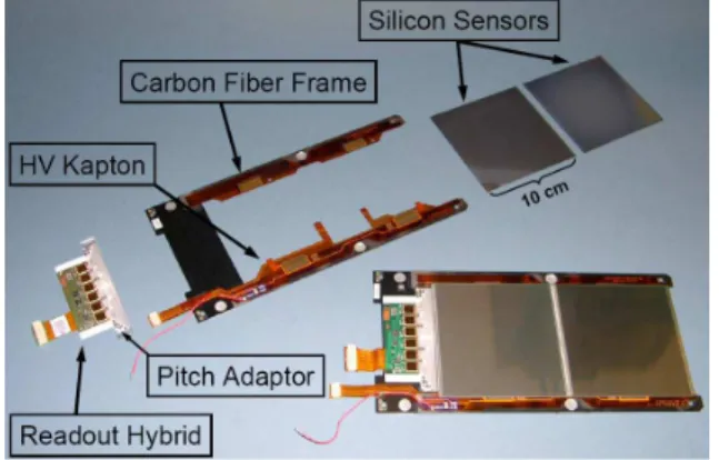
Figure 16: A CMS Module
The different parts forming a module are the frame of carbon fiber and Kapton, the hybrid with the front-end electronics and pitch adapter and the silicon sensors. Courtesy of colleagues from UCSB Santa Barbara, California.
populating the three inner silicon tracking layers of the CMS detector. With the pixelated structures, the chip covers the full sensor and a electronic to sensor channel connection is realized via bump bonding.
Pixel sensor High Densitiy Interconnect HDI
Token Bit Manager Signal Cable
SiN strips
Pixel Barrel Module
Bump bonding Voltage cable
Readout chips ROC
Figure 17: Pixel Module – barrel type [30]
1.5. Large Systems, Basic Strategies
The modules either directly mounted on the support structure (see sections2.2 and 2.3 or in the CMS case to larger substructures like rods or petals (see sec-
tion 2.4). Numerous geometrical arrangements exist, mainly forward walls in fixed target experiments or barrel structures, often with complementary forward wheels in the collider experiment to cover a maximumη-range. The purpose is to measure precise tracks of charged particles in a magnetic field. Initially, silicon trackers only complemented the more outer gas tracking detectors.
In the end, tracks allow
• the measurement of the particle’ momentumpT
– thus also the measurement of energy
• the identification of second and tertiary vertices.
• isolation of several particles with track close to each other
ThepT resolution and the impact parameter resolutionσd0, the parameter to identify secondary vertices, impose strong design criteria on any tracking device.
pT resolution. The transverse momentum resolutionp⊥ is defined by
∆p⊥
p⊥ ≈ ∆s[µm]
(L[cm])2B[T]p⊥[GeV] (13) with sagitta s = L2/8R, lever arm L, magnetic field B, curvature radius R and momentump⊥. The equation immediately tells, that (A) intrinsic position resolution has to be good to resolvesand that (B) the B field strength gives a linear improvement, while (C) a larger lever arm improves momentum resolution quadratically. An explanatory scheme is given in Fig. 18. With increasing p⊥
the resolution gets worse again and with an error of 100% not even the charge of the particle can be identified anymore. The superior point resolution of silicon
B IP R
L s
Figure 18:Transverse Momentum Resolutionp⊥
The momentum resolution of a moving charged parti- cle in a B field is given by its curvature path. With s=L2/8RandB·R=p/qone gets the momentum resolution as ∆pp ≈L∆s2Bp.
sensors with respect wire chambers clearly improves the impact parameter on the other hand, the lower lever arm in the LEP experiments need more outer gas tracking detectors. The early vertex detectors were more track seeders and vertex finders than tracking detectors. This changed with the CDF II upgrade and the current LHC detectors. Today, silicon trackers dominate the muon momentum resolution and are augmented only above several hundred MeV by the large ever arm of the outer muon detectors. For the energy resolution they are superior to the outer calorimeters for lower energies10.
10e.g. around 15GeV in the case of CMS
![Figure 9: Leakage Current vs. Fluence and Annealing Time[10, 9]](https://thumb-eu.123doks.com/thumbv2/1library_info/4364980.1576621/12.892.230.693.186.362/figure-leakage-current-vs-fluence-annealing-time.webp)
![Figure 10: Depletion Voltage Current vs. Fluence and Annealing Time[9]](https://thumb-eu.123doks.com/thumbv2/1library_info/4364980.1576621/13.892.205.714.189.375/figure-depletion-voltage-current-vs-fluence-annealing-time.webp)
![Figure 23: Reconstruction of the Production and Decay of a D − → K + π − π − as Measured in the NA11 Experiment in 200 GeV /c π − Be Interactions [17]](https://thumb-eu.123doks.com/thumbv2/1library_info/4364980.1576621/22.892.290.623.192.482/figure-reconstruction-production-decay-measured-experiment-gev-interactions.webp)
