DETECTOR FOR THE ILC
H.-G. Moser
1, L. Andricek
1, P. Fischer
3, F. Giesen
3, M. Harter
3, M. Karagounis
2, R. Kohrs
2, H. Krüger
2, G. Lutz
1, I. Peric
3, L. Reuen
2, R.H. Richter
1, C. Sandow
2, L. Strüder
1, J. Treis
1, M. Trimpl
2, N. Wermes
2, S. Wölfel
11
Semiconductor Laboratory of the Max-Planck-Institut für Physik and Max-Planck- Institut für extraterrestrische Physik, Otto-Hahn-Ring 6, D-81739 Munich, Germany
2
Physikalisches Institut der Universität Bonn Nussallee 12 D-53115 Bonn, Germany
3
Institut für Technische Informatik, B6, 26, D-68131 Mannheim, Germany
For the International Linear Collider a vertex detector with unprecedented performance is needed. The DEPFET, which integrates a MOSFET into the high resistivity detector substrate offers such performance: large signal/noise, small pixel size, thin detectors, low power consumption, high readout speed and radiation tolerance. This paper presents the concept of the DEPFET and results of a complete prototype system with dedicated control and readout electronics. Measurements of the radiation hardness will be presented and the technology to achieve thin detectors (50 μm) will be discussed.
1. Introduction
A vertex detector at the international linear collider [1] needs excellent position resolution (5 μm), fast readout (50 MHz) and radiation tolerance up to 100 kRad. The detector should introduce minimal scattering material, 0.1% X
0per layer at most. The DEPFET active pixel sensor offers a detector concept which can fulfill these requirements.
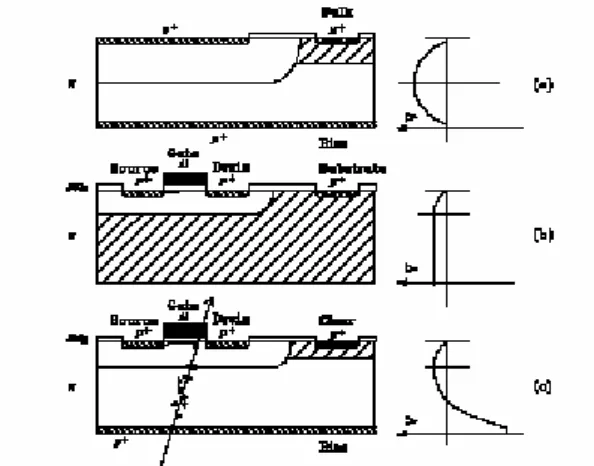
In the DEPFET Pixel concept [2], the first amplifying transistor is directly integrated into a high resistivity silicon substrate (Fig. 1). By sideward depletion and an additional n-implantation below the FET, a potential minimum for electrons is created underneath the transistor channel, which can be considered as an internal gate of the FET. The signal electrons created by an impinging particle are collected and stored in the internal gate, which results in a modulation of the transistor current. After readout the stored electrons are removed from the internal gate by a clear pulse. In this concept very good noise performance can be achieved. For ILC studies, prototype DEPFET pixel structures with dimensions of 22x30µm
2and matrix sizes of 64x128 pixels have
1
been devised. Dedicated steering (SWITCHER II) and readout ASICs (CURO- II) have been developed [3] optimized for the timing and speed requirements at an ILC. The matrix and electronics are arranged to allow parallel readout of the 64 columns for the pixels activated in a single row (Fig. 2).
Figure 1. The DEPFET detector and amplification structure is based on a sideward depleted substrate material (a) into which a planar field effect transistor (b) is embedded (a MOS device is shown here).
The electric potential is schematically drawn on the right side with the p+ implants set to ground.
n x m pixel
IDRAIN
DEPFET- matrix
VGATE, OFF off
off
off on
VGATE, ON
gate
drain
reset
VCLEAR, OFF reset
VCLEAR, ON off
off
off
VCLEAR-Control 0 suppression
output
Figure 2. DEPFET Matrix: The external gates and clear (“reset”) contacts are controlled in rows by SWITCHERs. The drain contacts are connected in columns to the CURO readout chip. This allows reading all pixels of a row in parallel.
2. Characterization of a Prototype in the Lab and Test Beams
Noise and clearing studies using single pixel devices and small mini pixel
matrices have been performed. The low intrinsic noise of the DEPFET could be
demonstrated in spectroscopic measurements of X-rays using special electronics with long shaping times (6 μsec). An ENC noise of 2.2 e
-at room temperature was measured [4]. To optimize the noise of the entire system under ILC timing conditions, the clearing noise must be minimized. As the readout cycle contains the sample (signal) clear (pedestal) sequence, clearing noise is minimal if the clear process fully empties the internal gate. It can be shown that over a large range of operating parameters a complete clearing can be achieved.
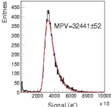
Figure 3. Signal distribution of 6 GeV electrons traversing a 450 μm thick DEPFET detector. The signal is from clusters defined by a 6 σ seed. Typical cluster sizes are 4-6 pixels. The peak value corresponds to 32441 e
-.
An ILC DEPFET Pixel prototype module with close to ILC specifications has been characterized by lab measurements and in a 6 GeV e
-test beam at DESY, Hamburg. All individual components have been shown to operate close to ILC timing requirements. In the test beam the system has been operated without on chip zero suppression and with slower speed, however. The noise of the total system with fast ILC shaping in the CUROII chip has been measured to 225 e
-. The signal for minimum ionizing particles in the 450μm thick detector corresponds to 32500 e
-(Fig. 3), resulting in a signal to noise ration of 144/ 1.
Scaling to the proposed thickness of 50μm gives S/N = 15/1. The position resolution has been measured to be 10μm, however, this value is dominated by the multiple scattering error due to the low energy beam.
3. Thinning Technology
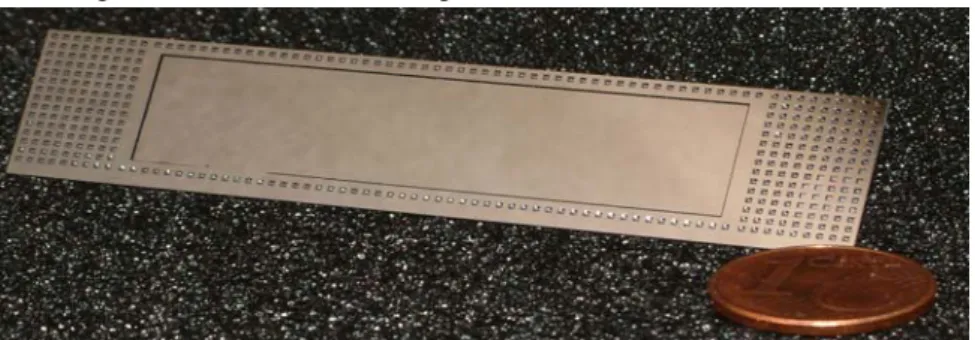
In order to reduce multiple scattering the material of the sensors must be
minimized. Using a wafer bonding technique it is possible to thin down the
active region of a DEPFET matrix to 50μm. Tests with diode structures showed
that the thinning did not deteriorate the performance of the device [5]. In order to achieve mechanical stiffness and stability a frame with the original thickness can be left over. Including this frame and electronics an effective thickness of 0.1% X
0can be achieved (Fig. 4). It should be stressed that the DEPFET technology allows producing large, self supporting, module size devices avoiding the need for extra mounting frames.
Figure 4. A silicon sample thinned down from 300μm to 50μm using the wafer bonding technique. A perforated frame has been left over to ensure mechanical stiffness.
4. Radiation Hardness
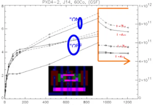
The inner layer will be exposed to 100 KRad in 5 years of ILC operation. Like all MOS devices, the DEPFET is inherently susceptible to ionizing radiation.
The predominant effect is the shift of the threshold voltage to more negative values due to the build up of positive oxide charges. Irradiations of such devices with hard X-Rays and
60Co Gamma rays up to 1MRad were performed under various biasing conditions. It turns out that the threshold shifts are small (~4V) and can be compensated without compromising the performance of the device (Fig. 5).
5. Power Consumption
In a DEPFET matrix only the single row which is actually read out dissipates
power: about 0.5W per row of 1000 pixels. In addition 6.3mW per active row
are dissipated by the switcher and 2.8W by the CURO readout chip. Taking into
account the duty cycle of the ILC accelerator, 1 ms beam followed by a pause of
199ms, a five layer detector as proposed in [1] would dissipate 3.1W. Only
0.5W is dissipated in the active area of the device. This reduces considerably the
cooling needs and allows for a low mass detector concept.
6. Conclusions
The DEPFET active pixel detector offers large signal/noise, fast signal collection, small pixel size and low power operation. The sensors can be thinned in order to introduce minimal scattering material. They are sufficiently radiation tolerant for ILC conditions. Control and readout ASICs performing close to ILC specifications has been developed. The system has been operated successfully in a test beam. Thus the DEPFET can be considered an ideal candidate for an ILC vertex detector.
"OFF
"ON
L=7μ L=6μ L=7μ L=6μ