Performance of a DEPFET pixel system for particle detection
M. Trimpl a ∗ , L. Andricek b , P. Fischer c , R. Kohrs a , H. Kr¨ uger a , G. Lutz b , H.G. Moser b , I. Peric c , L. Reuen a , R.H. Richter b , C. Sandow a , L. Str¨ uder d , J. Treis d , E. v. T¨orne a , J. Velthuis a , N. Wermes a
a Physikalisches Institut der Universit¨at Bonn, Nußallee 12, D-53115 Bonn, Germany
b Max-Planck-Institut f¨ ur Physik, F¨ohringer Ring 6, D-80805 M¨ unchen, Germany
c Institut f¨ ur Technische Informatik, B 6, 26, D-68131 Mannheim, Germany
d Max-Planck-Institut f¨ ur extraterrestrische Physik, Gießenbachstrasse 6, D-85478 Garching, Germany The DEPFET detector provides radiation detection and signal amplification by incorporating a field effect transistor in fully depleted silicon. Driven by the requirements of the ILC (International Linear Collider), a DEPFET pixel based prototype system has been developed. The system consists of a 64 × 128 pixel matrix with 28.5 × 36 µm 2 pixels, operated with two dedicated chips for a fast steering and readout. Results on the detection of X-rays in the energy range between 6 and 40 keV will be presented. For the first time, a DEPFET pixel system has been operated in a test beam. The paper will report on first results using the 6 GeV electron beam at the DESY synchrotron. The observed noise performance of the system will be compared with calculations. It will be shown that a noise figure of below ENC = 100 e − is achievable with DEPFET pixels for the ILC application leading to a signal-to-noise ratio of S/N > 40 for sensors as thin as 50 µm.
Keywords: Active Pixel Sensor, DEPFET, Linear Collider, ILC
1. Introduction
DEPFET active pixel sensors are used in a very broad field of application. The device com- bines a fully depleted detector for signal genera- tion by impinging radiation and a first amplifica- tion stage. The latter is realized by a field effect transistor integrated in every pixel cell [1]. Due to the internal amplification, excellent noise figures of the device, ENC = 2.2 ± 0.1 e − for 6 µs shaping time at room temperature, have been achieved so far [2]. Matrix systems based on DEPFET pixels have been successfully used in biomedical applications for the detection of tritium showing excellent imaging capabilities [3]. Furthermore, DEPFET pixels are a strong candidate for the wide field imager of the XEUS mission [4]. For the use in high energy physics particle tracking, where an excellent spatial resolution is required, linear DEPFET devices with pixel cells down to
∗ Corresponding author Marcel Trimpl, Tel.: +49-228-73- 3608; fax: +49-228-73-3220. E-mail address: trimpl@uni- bonn.de
a size of 22 ×36 µm 2 have been fabricated [5]. Ex- ploring their performance towards a micro vertex detector at the ILC, the radiation tolerance of the sensor against ionizing radiation has been shown up to a dose of 1 MRad using X-rays from a 60 Co source [6]. A thinning process for double sided silicon sensors has been developed [7] that can be adapted to a DEPFET pixel production. Hence, the fabrication of 50 µm thin detectors with a ra- diation length of only 0.1 % X 0 per sensor layer is possible. Providing a fully depleted sensor sub- strate, such thin DEPFET devices can achieve a signal-to-noise ratio of better than 40 with noise figures in the order of 100 e − .
2. The DEPFET principle
The principle of operation of the DEPFET is
illustrated in figure 1. A MOSFET embedded
into the silicon substrate is used for signal am-
plification. The detector substrate is depleted
by means of sidewards depletion. Supported by
a deep n implantation underneath the transis-
p+
p+ n+
rear contact
drain bulk
source
n
internal gate ext. gate
n
-p+
- -
+ + + +
- -
-
+ + + +
- 45 0
m
~1 m p- channel - - -- - - -
particle
Figure 1. Cross section of a DEPFET pixel through the transistor channel, illustrating the principle of operation.
tor channel, a potential minimum for electrons in formed which is known as the internal gate.
Charge generated by impinging radiation is sep- arated in the electric field. While the holes drift to the rear contact where they are removed, the electrons are accumulated in the internal gate.
The signal charge changes the potential of the internal gate which causes a modulation of the transistor current. The transistor current is mea- sured periodically and the accumulated charge during the integration time is obtained by sub- tracting two subsequent current measurements.
The conversion factor is known as the internal gain of the DEPFET device g q = dI/dQ, where dI is the change of the device current and dQ is the accumulated charge in the internal gate.
Due to the in-pixel amplification the input ca- pacitance of the amplifying transistor is kept very small and no external connection circuitry to the amplifier is needed. Both features enable a low noise operation of the device. However, for a very fast readout at the ILC vertex detector with line rates of 20 MHz and more, a noise performance of ENC ≈ 100 e − is targeted.
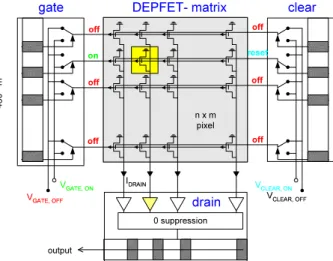
3. The DEPFET pixel system for particle tracking
Driven by the requirements of the ILC vertex detector [8], a DEPFET-system using a 64 × 128 pixel matrix has been developed. The system uti- lizes a 450 µm thick sensor because the thinning process of the wafer substrate has yet not been
n x m pixel
I
DEPFET- matrix
V
off
off on
off
V
gate
drain V
off
off reset
off
V
clear
output
0 suppression
Figure 2. Readout principle of a DEPFET pixel matrix in a row-wise operation mode with steer- ing chips at the side of the matrix and a readout chip at the bottom.
adapted to a DEPFET pixel production. In or- der to achieve the lowest possible power consump- tion and material budget in the sensitive area, a readout concept has been chosen where the ma- trix is operated row-wise. The row-wise opera- tion mode is illustrated in figure 2, where pixels in the matrix are addressed like in a RAM struc- ture: One row is selected after each other and the pixel currents are read out column wise in paral- lel at the bottom of the matrix. For this purpose a fast steering chip SWITCHER II and readout chip CURO II have been fabricated [9]. Figure 3 shows a photograph of the DEPFET pixel system.
With steering chips attached at both sides of the matrix this prototype system has been designed to be very versatile. As shown in [10], future sys- tems can be operated with only one steering chip.
4. Results
The results presented in this section have been
achieved by operating the system at a line rate of
0.9 MHz. Although the standalone performance
of the single components of the system (fast clear
of the DEPFET matrix, the steering and readout
chip) is compatible with a line rate of 20 MHz,
as required at the ILC, the timing between the
components has not yet been optimized, so that
Figure 3. Photograph (area shown: 23 × 16 mm 2 ) of the 64 × 128 DEPFET pixel system with the sensor matrix in the center, two steering chips (SWITCHER II) located at both sides and the readout chip (CURO II) at the bottom.
a slower readout speed was chosen.
4.1. System performance for X-ray detec- tion
The system has been tested using X-rays with an energy of 5.9 keV up to 44.23 keV using differ- ent radioactive sources.
To determine the internal gain of the DEPFET device and to measure the linearity of the sys- tem energy spectra have been taken for Rubidium (Rb), Molybdenum (Mo), Silver (Ag), Cadmium (Cd), Barium (Ba) and Terbium (Tb) provided by a variable X-ray source. After performing a row-wise common mode correction 2 , clusters are reconstructed by identifying neighboring pixels, where every pixel contains a signal higher than five times its noise. In figure 4 the mean cluster signal as a function of the characteristic X-ray energy is shown. From the slope of the system response an internal gain of the DEPFET sen- sor of g q = 282.6 ± 3.3 pA/e − is extracted. The integral-non-linearity (INL) of the system is bet- ter than 0.8 % for a dynamic range of 8500 e − , which is large enough for the detection of about 2 MIPs in a 50 µm thin sensor device.
The capability of spatial detection of X-rays
2 Subtraction of a mean value (common mode) from the pixel pedestal. The common mode is computed using the pedestals of each pixel of a row that contain no signal.
10 15 20 25 30 35 40 45
500 1000 1500 2000 2500 3000 3500
s ig n a l [n A ]
E [keV]
Ag/Cd
Ba
Tb
Rb Mo
Figure 4. Linearity of the DEPFET Pixel Sys- tem. The sensor output is shown for different radioactice sources.
Figure 5. Radiogram of a 75 µm thick tungsten test chart taken with 55 Fe.
has been demonstrated using a 75 µm thick tung- sten test chart with an engraved logo and sev- eral MTF line structures having a pitch of 100, 75, 50 and 25 µm (from left to right respectively).
The radiogram of the 2 x 3 mm 2 large test chart is shown in figure 5. It has been taken by plac- ing the test chart on the backside of the detector and irradiating the system with a 55 Fe source.
The radiogram has been obtained by summing
the pulse heights for pixels that contain a signal
higher than five times their noise. Although no
spatial reconstruction techniques have been ap-
plied to improve the spatial resolution, the 50 µm
lines in the radiogram are clearly visible.
Figure 6. Testbeam setup at the DESY syn- chrotron.
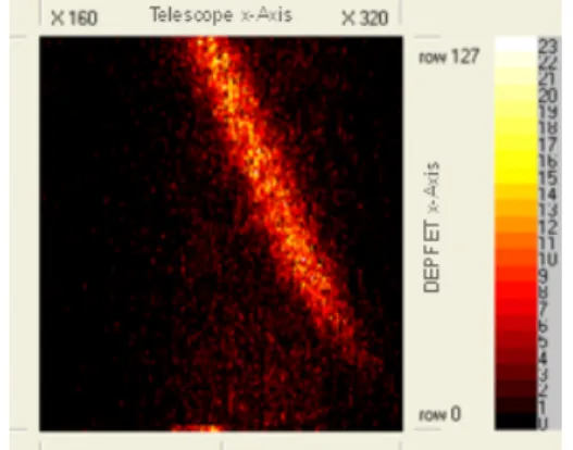
Figure 7. Correlation between one telescope plane and the DEPFET sensor.
4.2. First test beam results
The complete system has been operated in the 6 GeV electron test beam at the DESY syn- chrotron. The setup, shown in figure 6, consists of 4 microstrip telescope modules [11], the DEPFET system and several scintillator trigger counters.
During the beam period a firm correlation be- tween the sensor response and the telescope mod- ules was observed. An example is shown in figure 7 for the x-coordinate. The raw data spectrum after pedestal subtraction and common mode correction is shown in figure 8. The to- tal noise of the system, determined by the width of a Gaussian fitted to the noise peak is found to be ENC = 225.03 ± 0.02 e − at room temperature.
Due to the common mode correction the noise fig- ure of the system has been improved by a factor of three. Therefore, an on-chip common mode correction will be implemented in the next gener- ation of the readout chip. The noise performance will be discussed in section 4.3. To reconstruct clusters, seed pixels showing a signal ∼ 6 times
Figure 8. Raw data spectrum obtained in the test beam after pedestal subtraction and common mode correction.
higher than their noise are identified and are com- bined into a cluster with their neighboring pixels if their signals are 2 times higher than their noise.
The signal distribution for clusters of maximum 3 ×3 pixels is given in figure 9 for a seed threshold of 1500 e − . The most probable signal extracted by fitting a landau distribution is found to be 32446 ± 52 e − . With an observed noise figure of
≈ 225 e − , this converts to a signal-to-noise ratio of S/N=144.2 ± 0.2. A more detailed discussion of the test beam analysis is presented in [12].
4.3. Estimation of the noise performance In this section the noise performance of the sys- tem will be calculated and compared with the ob- served value. The noise contribution of the steer- ing chip, the readout chip and the sensor matrix will be discussed separately.
Steering chip
A simplified output stage of the steering chip,
SWITCHER II, is shown in figure 10 where the
gate voltage is multiplexed to a matrix row by
a pass transistor. The dominant noise contribu-
tion of the steering chip is due to thermal noise
of the pass transistor: V R 2 = 4kTR S . Since the
noise voltage is filtered by the switch resistance
R S and the capacitive load of a matrix row C row ,
the resulting noise is of kT/C-nature and de-
pends only on the capacitive load. For a typical
Figure 9. Cluster signal distribution for a maxi- mum of 3×3 pixel cluster. A landau function has been fitted to the distribution.
!"#
$%
&
'())
*+,-./
-01
2345 6 78
9:+;;<=