The MOS-Type DEPFET Pixel Sensor for the ILC Environment
L. Andriceka,*, P. Fischerb, K. Heinzingera, S. Herrmanna, D. Herza, M. Karagounisc, R. Kohrsc, H. Krügerc, P. Lechnera, G. Lutza, H.-G. Mosera, I. Pericb, L. Reuenc, R.H. Richtera, C. Sandowc, M. Schneckea, F. Schoppera, L. Strüdera, E. v. Törnec,
J. Treisa, M. Trimplc, J. Velthuisc, N. Wermesc, and S. Wölfela
aMPI Halbleiterlabor, D-81739 Munich, Germany
bMannheim University, D-68159 Mannheim, Germany
cBonn Unversity, D-53112 Bonn, Germany
Elsevier use only: Received date here; revised date here; accepted date here
Abstract
A new generation of MOS-type DEPFET active pixel sensors in double metal/double poly technology with ~25µm pixel size has been developed to meet the requirements of the vertex detector at the ILC (International Linear Collider). The paper presents the design and technology of the new linear MOS-type DEPFET sensors including a module concept and results of a feasibility study on how to build ultra-thin fully depleted sensors. One of the major challenges at the ILC is the dominant e+e- pair background from beam-beam interactions. The resulting high occupancy in the first layer of the vertex detector can be reduced by an extremely fast read out of the pixel arrays but the pair-produced electrons will also damage the sensor by ionization. Like all MOS devices, the DEPFET is inherently susceptible to ionizing radiation. The predominant effect of this kind of irradiation is the shift of the threshold voltage to more negative values due to the build up of positive oxide charges.
The paper presents the first results of the irradiation of such devices with hard X-Rays and Gamma rays from a 60Co source up to 1Mrad(Si) under various biasing conditions. © 2001 Elsevier Science. All rights reserved
Keywords: DEPFET; APS; ILC; Vertex Detector; radiation tolerance; ionizing radiation
1. Introduction
Higgs, SUSY and heavy flavor physics are central themes in future linear colliders. They require precise vertexing and b-quark tagging using low momentum tracks. As a consequence the tracking detectors have to be put as close as possible to the primary interaction point and the multiple scattering has to be
kept as small as possible. Fine granularity pixel detectors and sufficiently high readout speed are required in order to resolve closely spaced tracks and in order to limit occupancy to a tolerable level. Power consumption has to be kept small in order to avoid the introduction of additional material for cooling. In the following a solution is presented which is able to meet these requirements. It is based on the DEPFET structure[1], a concept which fulfills the function of detector and amplifier simultaneously. The DEPFET
NUCLEAR INSTRUMENTS
& METHODS IN PHYSICS
RESEARCH Section A
* Corresponding author. Tel.: +49-89-839400-55; fax: +49-89-839400-13; e-mail: lca@hll.mpg.de.
can be used as the first amplification stage in the center of a Silicon Drift Detector[2] or as a pixel cell in matrices designed for a variety of applications ranging from X-ray spectroscopy and imaging[3] to tracking of charged particles for the future International Linear Collider (ILC). This paper presents in section 2 briefly the main features of the MOS-type DEPFETs designed for the ILC vertex detector, together with our approach for the production of thin wafer-scale matrices. Section 3 addresses the tolerance of MOS-type DEPFETs against ionizing radiation.
2. The DEPFET Pixel Cell and Module Concept The vertex detector for the International Linear Collider ILC (see e.g. [4] for further details) will be a set of cylindrical detectors arranged in ladders around the interaction point. Each ladder is an array of pixel cells read out at the end of the ladder outside the sensitive volume. In the case of a DEPFET as the pixel cell, the signal charge is measured in every pixel on a row-by-row basis and the DEPFETs are successively switched on by means of gating lines controlled by shift registers located at the long side of the ladder.
Fig. 1. Linear DEPFET topology for Linear Collider application
The MOS-type DEPFET is integrated on a fully depleted silicon substrate. All the charge generated by a traversing particle drifts due to the electric field configuration inside the device toward the surface and is collected in a potential minimum for electrons underneath the external gate of the DEPFET. The charge cloud is stored and modulates the current in the channel of the FET which forms in this way the first amplification stage. After signal read out is
finished, the charge is removed by applying a positive voltage to the “Clear” contact (see Fig.1).
The combination of the detector material and first amplification stage in one single device has a number of advantages. The sensitivity of the entire bulk and the low capacitance of the read out node enable low noise operation over a large range of temperatures.
This is of particular interest for applications at linear collider experiments where the sensors have to be as thin as possible. A second important point is that the charge is measured at the place of generation and has not to be transferred to the readout nodes at the edges of the sensitive region (like in CCDs), so trapping due to bulk damage by Non Ionizing Energy Loss (NIEL) is of minor importance. And finally, since the transistors can be turned off during charge collection and since only one row is electrically active during read out, the expected power consumption in the sensitive area is extremely low. Assuming ID=30 µA at VDS=-5V for the DEPFET pixel during read out, we expect a total power dissipation of about 21W for the 120 modules with roughly 800 Mpix in the sensitive DEPFET pixel area of the entire vertex detector. This is reduced by a factor 1/200[4], taking advantage of the duty cycle at the ILC. In addition to this, there is the power dissipated by the external steering and read out chips[5].
Fig. 2. Module concept for the first layer of the vertex detector at the ILC.
In our concept the DEPFET pixel array is made on thin (50 μm) detector grade silicon supported by a directly bonded silicon frame of 300 μm thickness.
Fig.2 shows the sketch of such a module for the innermost layer at the ILC. The averaged material contribution of the ladder in the sensitive area is 0.11% X0, including the frame and the (also back thinned to 50 μm) steering chips at the edge. The
details of the read out and steering chips as well as the system aspects can be found in [5] and [6]. The latest results of system and beam tests will be the topic of a dedicated paper at this conference[7].
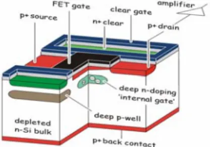
2.1. DEPFET Technology and Single Pixel Results Fabrication of large wafer scale pixel matrices demands a fault-tolerant and reliable technology. The availability of more than one metal layer is mandatory due to the necessity of the row- and column-wise connections of the pixels. As a result a new technology with two poly-silicon and two metal layers was introduced at the MPI Semiconductor Laboratory[8]. In order to guarantee a high homogeneity with respect to the operating parameters of the individual cells of the entire matrix, a MOS- type DEPFET was chosen as the pixel cell. Fig. 3 shows a cross section through a DEPFET cell perpendicular to the transistor channel leading from the p-doped channel (right) to the n+ doped clear contact. The n-doped internal gate is located underneath the transistor channel, which is separated from the “Clear” contact by the poly-silicon “Clear Gate”.
Fig. 3. Double poly-silicon and double metal technology for MOS-type DEPFETs.
Fig. 4 is a micrograph showing a section of the latest production of DEPFET arrays. The two orthogonal aluminium layers are the horizontally running Gate, Clear and Clear Gate lines and the vertical Drain and Source lines. There is a deposited silicon oxide layer as the interlevel dielectric in- between.
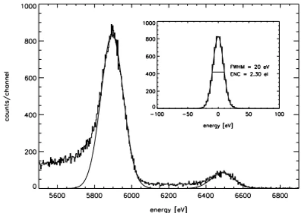
Single cell double pixel structures of linear MOS- type DEPFETs (gate length L=7μm, gate width W=25μm) designed for the ILC have been tested with an 55Fe source for their spectroscopic performance.
Fig. 4. Micrograph of a section of the DEPFET matrix in double metal technology. The red frame represents one pixel cell.
The drain current was read out with a conventional low cost operation amplifier operated as a current-to- voltage converter and followed by a spectroscopy shaping amplifier with a shaping time of 6µs. The signal was then digitized by a commercial ADC in peak sensing mode. The obtained spectrum is shown in Fig.5. In this read out mode we find an equivalent noise charge in the noise peak of 2.3e- (rms) and a full width at half maximum of 143eV of the Mn-Kα line (5.9 keV) at room temperature. These results clearly show the potential of the new MOS-type DEPFETs for both X-ray spectroscopy and efficient vertexing with thin sensors at the ILC.
Fig. 5. 55Fe spectrum taken with a linear MOS-type DEPFET (gate length L=7μm, gate width W=25μm) in drain current read out at room temperature. The insert shows the noise peak with an ENC(rms)=2.3e- .
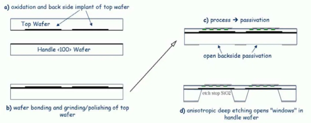
Fig. 6. The process sequence for production of thin silicon sensors with electrically active back side implant starts with the oxidation of the top and handle wafer and the back side implantation for the sensor devices(a). After direct wafer bonding, the top wafer is thinned and polished to the desired thickness(b). The processing of the devices on the top side of the wafer stack is done on conventional equipment; the openings in the back side passivation define the areas where the bulk of the handle wafer will be removed(c). The bulk of the handle wafer is removed by deep anisotropic wet etching. The etch process stops at the silicon oxide interface between the two wafers(d).
2.2. Thinning Technology
Back thinning of ASICs is already widely used in semiconductor industry. However, these technologies are not applicable for fully depleted sensors with an electrically active backside. Fig.6 illustrates the thinning technology based on direct wafer bonding[9]
and deep anisotropic etching to build such thin devices with a minimum of processing steps after thinning.
The feasibility of this approach has been shown with the production of 50 μm thin PiN diodes (see Fig.7). The volume generated reverse current of the thin devices is with <1nA/cm2 extremely encouraging. The mechanical stability of the diced chips is even for wafer scale devices sufficient for safe handling and mounting. There is no distortion visible on the 50 μm thin large area (6.5cm2) silicon membrane with single sided aluminium metallization.
A detailed description of the process can be found in[10]. Wafer bonding, grinding and polishing is done with an industrial partner. The integration of the technology in the production line at the MPI Semiconductor Laboratory is well under way.
Fig. 7. Top (left) and handle wafer side (right) of two diced chips (1 cm2) with four 10 mm2 PiN diodes on 50 μm thin silicon.
3. Radiation Tolerance of the MOS-type DEPFET The dominant background of pair-produced electrons which penetrate the inner layer of the vertex detector at the ILC imposes a requirement on radiation hardness of about 100krad for a 5 year life time[2]. In addition there is NIEL (Non Ionizing Energy Loss) damage due to the neutron background which is estimated to be at the level of 109 1MeV- neutrons/cm2 per year.
Table 1.
List of the irradiated devices
Wafer Transistor L (μm) W(μm) Source Biasing during
irradiation
PXD4-1 T60-1 60 120 X-ray(Mo) All terminals grounded
PXD4-1 T60-2 60 120 X-ray(Mo) All terminals grounded
PXD4-1 T60-3 60 120 X-ray(Mo) All terminals grounded
PXD4-2 T10-1 10 120 X-ray(Mo) Transistor „off“
PXD4-2 T20-1 20 120 X-ray(Mo) Transistor „off“
PXD4-2 A2-1 6 25 60Co Transistor „off“
PXD4-2 B2-1 6 25 60Co Transistor „off“
PXD4-2 D2-1 6 25 60Co Transistor „on“
PXD4-2 A2-2 7 25 60Co Transistor „off“
PXD4-2 B2-2 7 25 60Co Transistor „off“
PXD4-2 D2-2 7 25 60Co Transistor „on“
PXD4-3 T5-1 5 120 X-ray(Mo) first „off“, then „on“
Since there is no charge transfer during operation of DEPFET matrices, damage of the silicon bulk due to NIEL is of minor importance for this kind of devices. However, all MOS technologies are inherently susceptible to ionizing radiation. The main total ionizing dose effects are
• the shift of the threshold voltage to more negative values caused by radiation induced charge build up in the oxide and interfacial regions,
• build up of states at the interface between Si and SiO2 resulting in an increased sub-threshold slope and possibly a higher 1/f noise,
• reduction of the transconductance (gm) due to a lower mobility of the charge carriers in the channel after irradiation.
The degradation of MOS transistors with a certain thickness of the gate dielectrics (more than 200 nm in the case of the DEPFET) and for a given total ionizing dose in the oxide depends in the first place on the technology and the biasing conditions during irradiation[10].
3.1. Irradiation Conditions
Twelve DEPFET MOS-type test devices from three different wafers of the current production have been irradiated with 60Co gamma radiation and hard X-rays from an X-ray tube with Molybdenum target to investigate the radiation tolerance of the current technology. The devices under test are exactly the same double-pixel DEPFETs like in the main matrix[8], except for the gate area (gate length L=5µm - 60µm and width W=25µm - 120µm).
During normal operation at the ILC, the DEPFET is in “charge collection mode”, i.e. fully depleted bulk with empty internal gate and switched off by applying a positive gate voltage with respect to the source. The transistors of a row are only switched on during the short read out period. The time ratio between “off” and “on” state toff/ton in the first layer of the ILC vertex detector (assuming a 512x4096 pixel array read out at both sides) is in the order of 1000. Thus the irradiation of six test devices was done with the transistors in “off” state with an empty internal gate to test for the radiation tolerance in this most frequent operation mode. To investigate the implication of the biasing conditions on radiation tolerance, some transistors were also
irradiated in “on” state, others with all terminals grounded, and one transistor being first in “off”
state then switched to “on” during irradiation. Table 1 lists the irradiated devices, the irradiation source, and the biasing conditions during irradiation.
3.2. Results and Discussion
For the 60Co irradiation, the dose rate was 20 krad(Si)/h. The dosimetry was provided by colleagues of the National Research Centre for Environment and Health (GSF) by means of a calibrated ionization chamber. The input characteristic of the devices were measured immediately (approximately 1 min) after each irradiation period and the threshold voltage was extracted by a quadratic extrapolation of the IDrain(VGate) curve to IDrain=0.
a., b.
c., d.
e.f.
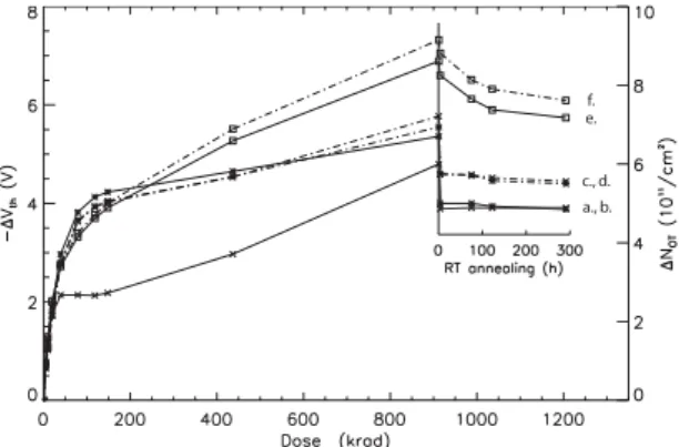
Fig. 8. Threshold shift and generated oxide trapped charge Not
during 60Co irradiation and after short term annealing at room temperature. The curves a., b., c., and d. are from four DEPFETs irradiated in “off” state (A2-1, A2-2, B2-1, B2-2), the two curves labeled e. and f. are from DEPFETs irradiated in “on” state (D2- 1, D2-2). Solid lines from DEPFETs with gate length L=6μm, dash-dotted lines from the ones with L=7μm.
Fig.8 shows the threshold voltage shift and the density of the oxide trapped charge Not of six DEPFETs, four biased in “off” state and two in
“on” state during irradiation, as a function of the total ionizing dose. The irradiation was stopped after 912krad(Si) and the devices were held under bias for annealing at room temperature. For the transistors irradiated in “off” state, most of the annealing took place in the first 3.5h and the
threshold voltage shift reaches a stable value of around -4V. The DEPFETs irradiated in “on” state are less radiation tolerant and the annealing has a longer time constant. The threshold voltage shift after 294.5 h annealing at room temperature is about -6V in this case. This difference can be attributed to different field configurations in the gate oxide[11].
Please note that identical DEPFETs under the same biasing conditions during irradiation have almost the same threshold shifts after irradiation and short annealing. The systematic difference between the DEPFETs with a gate length of L=6 μm and the ones with L=7 μm (full and dash-dotted lines in Fig.8) is not yet fully understood and still under investigation.
a.
b.
c.
Fig. 9. Threshold shift for the transistors T10-1 and T20-1 being in “off“ state during irradiation (a.), the transistor T5-1 being in
“off” state for 360krad(Si) and then switched on for remaining irradiation up to 1.2Mrad(Si) was reached (b), and the transistors T60-1, T60-2, and T60-3 with all terminals grounded (c.).
In order to cross check these results, the irradiations were repeated using the in house available CaliFa[12] irradiation facility with an X- ray tube with Mo target operated at 30kV. The spectrum of the radiation is given by bremsstrahlung with the characteristic energy peak at 17.44keV of Molybdenum. The dosimetry is based on the measured spectrum and the known absorption coefficient of SiO2[12]. The dose rate for this irradiation was lower (9krad/h) and there was an annealing step for 18h to 24h after each irradiation step. The results are shown in Fig.9.
Comparable devices, biased in the same way
(curves a. Fig.9), show about the same threshold shifts as in the previous irradiation. DEPFET T5-1, curve b in Fig.9, was first irradiated in “off” state up to 360krad(Si) and then turned on during irradiation. The curve shows clearly the effect of the biasing condition during irradiation.
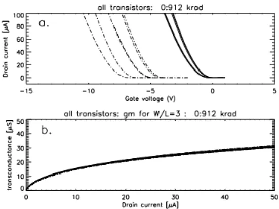
Fig. 10 Input characteristics of six (A2-1, A2-2,B2-1, B2-2, D2- 1, D2-2) DEPFETs before (solid lines) and after (dashed lines) a total ionizing dose of 912krad(Si) 60Co irradiation (a.) and transconductance normalized to W/L=3 of all six transistors before and after irradiation (b.).
The transconductance gm did not change after irradiation with 60Co. This can be seen in Fig.10a, where input characteristics of the six DEPFETs (A2-1, A2-2, B2-1, B2-2, D2-1, D2-2) are shown, both before and after irradiation. The threshold voltage shifts to more negative values but the slope stays almost constant. This fact is much better visible in Fig.10b where the transconductance gm
normalized to W/L=3 is plotted as a function of the drain current.
And finally, since the most important issue is the spectroscopic performance (signal/noise ratio) of the DEPFET after irradiation, Fig.11 shows an 55Fe spectrum taken with the irradiated device A2-2 at room temperature. It was done with the same setup and same settings for the spectroscopy amplifier used for the spectrum shown in Fig. 5. The equivalent noise charge of the noise peak is now 7.9 e- (rms) and the full width at half maximum of the Mn-Kα line is 174 eV. Even after this high total ionizing dose of almost 1 Mrad(Si), the DEPFET shows only a moderate noise increase of about 6 electrons equivalent noise charge.
Fig. 11. 55Fe spectrum taken with a linear MOS-type DEPFET (gate length L=7μm, gate width W=25μm) in drain current read out at room temperature after irradiation with a total ionizing dose of 912 krad(Si). The inset shows the noise peak with an ENC(rms)=7.9e-. Full width at half maximum of the Mn-Kα line is 174 eV.
4. Conclusions
The MOS-type DEPFET with its spectroscopic performance is a promising candidate to fulfill the challenging requirements for the vertex detection at the future linear collider ILC. The requirement of a minimal material budget is addressed by intrinsically low power dissipation, thereby saving material for cooling structures. The extremely low noise of the device offers the advantage to build very thin sensors with still very good signal/noise ratios. The feasibility of the technology for the production of thin DEPFET arrays was shown with the successful manufacturing of 50 µm thin PiN diodes.
Based on the irradiation results we conclude that DEPFETs biased accordingly to the operating conditions in the experiment are remarkably radiation tolerant. After a total ionizing dose of 1 Mrad(Si), which corresponds to a safety factor of 10 for a 5 year operation in the first layer of the vertex detector at the ILC, the threshold voltage shift is only about -4V. The shape of the DEPFET input characteristic and the transconductance are not affected by the irradiation. Hence the radiation induced threshold voltage shift can simply be compensated by a gradual decrease of the gate
voltage needed for the selection of a pixel row. This relatively small shift of a few Volts is within the voltage range available with the steering chips for the row selection. Although based on a limited number of irradiated devices, it can be stated, that identical DEPFETs biased in the same way during irradiation have very similar characteristics after irradiation.
There is a moderate increase of noise of about 6 electrons equivalent noise charge after a total ionizing dose of almost 1 Mrad(Si). But as the noise level with the fast read out needed at the ILC vertex detector is expected to be in the order of 100 electrons equivalent noise charge[5], the small additional noise stemming from an irradiated DEPFET is not considered as the limiting factor.
Acknowledgments
The authors would like to thank C. Hoeschen and W. Panzer at the Institute of Radiation Protection of the National Research Centre for Environment and Health (GSF) in Munich for the support and opportunity to use their 60Co irradiation facility ELDORADO.
References
[1] J. Kemmer, G.Lutz, "New Detetecor Concepts", Nucl.
Instrum. Methods, vol A253, pp. 365-377, 1987
[2] C. Zhang, P. Lechner, G. Lutz, M. Porro, R.H. Richter, J.
Treis et al., " Development of DEPFET Macropixel Detectors", presented at the 10th Symposium on Semiconductor Detectors, Wildbad Kreuth, June 2005, submitted to Nucl. Instrum. Methods A
[3] J. Treis, P. Fischer, O. Haelker, M. Harter, S. Herrmann, R.
Kohrs, et al., "DEPMOSFET Active Pixel Sensor Protoypes for the XEUS Wide Field Imager", IEEE Trans.
Nucl. Sci. Vol 52, No.4, August 2005
[4] T. Behnke, S. Bertolucci, R. D. Heuer, and R. Settles, Eds.,
"TESLA Technical Design Report, Part IV: A Detector for TESLA", DESY, Hamburg, Germany, DESY 2001-011, March 2001
[5] R. Kohrs, L. Andricek, P. Fischer, M.Haerter, M.
Karagounis, H.Krueger et al, "Development of a Prototype Module for a DEPFET Pixel Vertex Detector for a Linear Collider", IEEE Trans. Nucl. Sci., Vol. 52, No. 4, August 2005
[6] M. Trimpl, L. Andricek, P. Fischer, G. Lutz, R.H. Richter, L. Strueder, et al., "A Fast Readout using Switched Current
Techniques for a DEPFET Pixel based Vertex Detector for TESLA", Nucl. Instrum. Methods, vol. A511, pp. 257-264, 2003.
[7] R.Kohrs et al., "A DEPFET Prototype System for the ILC Vertex Detector: Lab and Test beam Measurements", presented at the PIXEL2005 Workshop, Bonn, September 2005, submitted to Nucl. Instrum. Methods A
[8] R.H. Richter et al., “Design and technology of DEPFET pixel sensors for linear collider applications”, Nucl.
Instrum. Methods, vol. A511, pp. 250-256, 2003.
[9] Q.Y. Tong, U. Goesele, Semiconductor Wafer Bonding, New York: John Wiley & Sons, 1999.
[10] L. Andricek et al., "Processing of ultra-thin silicon sensors for future e+e- linear collider experiments", IEEE Trans.
Nucl. Sci. Vol 51, No.3, June 2004, pp 1117-1120 [11] T.P. Ma, P. Dressendorfer, Eds., "Ionizing Radiation
Effects in MOS devices and circuits", John Wiley&Sons, New York, 1989.
[12] A. Pahlke, "Einfluss der Oxidqualität auf die Stabilität von Halbleiterdetektoren bei Röntgenstrahlung", Ph.D. Thesis, TU München, 2003