Nuclear Instruments and Methods in Physics Research A 579 (2007) 685–689
DEPFET, a monolithic active pixel sensor for the ILC
$J.J. Velthuisa,, R. Kohrsa, M. Mathesa, A. Rasperezae, L. Reuena, L. Andricekc, M. Kocha, Z. Dolezald, P. Fischerb, A. Freye, F. Giesenb, P. Kodysd, C. Kreidlb, H. Kru¨gera,
P. Lodomeza, G. Lutzc, H.G. Moserc, R.H. Richterc, C. Sandowa, D. Scheirichd, E. von To¨rnea, M. Trimpla, Q. Weic, N. Wermesa
aUniversity of Bonn, Physikalisches Institut, Nussallee 12, D-53115 Bonn, Germany
bUniversity of Mannheim, B6 26, D-68161 Mannheim, Germany
cMax Planck Institute Semiconductor Laboratory, Otto-Hahn-Ring 6, D-81739 Mu¨nchen, Germany
dCharles University, Institute of Particle and Nuclear Physics, V. Holesovickach 2, CZ-18000 Praha, Czech Republic
eMax-Planck-Institut fu¨r Physik, Fo¨hringer Ring 6, D-80805 Mu¨nchen, Germany Available online 26 May 2007
Abstract
In a DEPleted Field Effect Transistor (DEPFET) sensor a MOSFET is integrated on a sidewards depleted p-on-n silicon detector, thereby combining the advantages of a fully depleted silicon sensor with in-pixel amplification. A 450mm thick DEPFET was tested in a testbeam. TheS/Nwas found to be larger than 110. The position resolution is better than 5mm. At a seed cut of 7s, the efficiency and purity are both close to 100%. In the readout chip a zero-suppression capability is implemented. The functionality was demonstrated using a radio-active source. The predicted impact parameter resolution of a 50mm thick DEPFET vertex detector, is much better than required for the International Linear Collider (ILC).
r2007 Elsevier B.V. All rights reserved.
PACS:29.90.W; 29.40.G; 42.79.P
Keywords:Active pixel sensors; CMOS; Tracking; Solid state detectors
1. Introduction
For the accurate measurement of Higgs branching ratios and properties as well as precise studies of physics processes beyond the Standard Model at the International Linear Collider (ILC), efficient distinction of heavy quark flavors, most notably of bottom and charm quarks, is a must. This requires precise secondary and even tertiary vertex detection, correct assignment of every track to the correct vertex and determination of the jet charge.
Since the impact parameter of b-quarks is in the order of 300mm and of c-quarks 100mm, the challenge for a vertex detector at the ILC is to build a very low mass, high
precision vertex detector. The aims are a single hit resolution better than 5mm and a radiation length less than 0.1% X0 for a ladder, which requires 50mm thick silicon sensors. The very low mass requirement implicates that no active cooling can be used. Therefore, the detectors power consumption is limited to amounts that can be removed by flowing gas through the detector.
Due to the very high beamstrahlung rate near the interaction point, which produces e+e-pairs in vast numbers, the background conditions and the time structure of the accelerator are leading to detector occupancies of 100 hits/mm2/bunch train (1 ms) for a pixel detector situated 15 mm away from the beam line [1].
Also the time structure of the ILC provides a challenge.
There will be 2820 bunches per pulse, which are spaced 337 ns apart, leading to a pulse train of 950ms which has a repetition rate of 5 Hz. The aim is to readout the sensors 20 times during a bunch train. In our current design this
www.elsevier.com/locate/nima
0168-9002/$ - see front matterr2007 Elsevier B.V. All rights reserved.
doi:10.1016/j.nima.2007.05.278
$This work was supported by the Alexander von Humboldt Founda- tion, Germany.
Corresponding author. Tel.: +49228733608.
E-mail address:velthuis@physik.uni-bonn.de (J.J. Velthuis).
requires a row readout rate of 20 MHz. To limit the power consumption the readout chips need to be switched off in between the bunch trains. The radiation load is modest.
The detector has to withstand 200 krad for 5 years operation[2].
The DEPleted Field Effect Transistor structure, abbre- viated DEPFET [3], provides detection and amplification properties together. The principle of operation is shown in Fig. 1. A MOS or junction field effect transistor is integrated onto a detector substrate. By means of side- wards depletion, appropriate bulk, source and drain potentials, and an additional deep-n-implantation, a potential minimum for electrons is created right under- neath the transistor channel (1mm below the surface).
This can be regarded as an internal gate of the transistor. A particle entering the detector creates electron–hole pairs in the fully depleted silicon substrate. While the holes drift to the rear contact of the detector, the electrons are collected in the internal gate where they are kept stored. The signal charge leads to a change in the potential of the internal gate, resulting in a modulation of the channel current of the
transistor. The signal charges are cleared out of the internal gate by a positive voltage at the CLEAR contact. Note that the signal is not destructed by the readout until the clear pulse is issued, hence allowing multiple readout.
The low noise is obtained because of the small capacitance of the internal gate (several 10 fF) and the absence of external connections to the first amplification stage. The high signal is due to the charge collection in a fully depleted bulk. Both together yield a very large S/N
Fig. 1. DEPFET principle.
Seed cut (σ)
0 10 15 20 25 30 35 40
Efficiency (%)
97.5 98 98.5 99 99.5 100
Standard efficiency Applying modest χ2 cut
Seed cut (σ)
0 8 10 12 14 16 18 20
Purity (%)
50 60 70 80 90 100
2 4 6
5
Fig. 2. Efficiency and purity as a function of the seed cut.
Threshold (DAC)
5 10 15 20 25 30 35 40 45
DEPFET Occupancy (%)
0 2 4 6 8 10
with source no source
Fig. 3. Entire DEPFET occupancy as a function of the threshold with and without a radio-active source, demonstrating that the zero-suppression works. Note that the occupancy is limited by the buffer size.
ratio. For particle detection at the ILC the use of very thin (50mm) detectors, still operated with large S/N figures and a very low power consumption, are targeted.
2. Current status
Many of the ILC requirements have already been addressed. For instance, the radiation tolerance against Cluster size (pixel)
0 5 10 15 20 25 30 35
Entries
0 100 200 300 400 500 600 700 800
900 φ =0
φ =10 φ =20 φ =30 φ =40
φ =0 φ =10 φ =20 φ =30 φ =40
φ =0 φ =10 φ =20 φ =30 φ =40 φ =0
φ =10 φ =20 φ =30 φ =40
Cluster size (pixel)
0 5 10 15 20 25 30 35
Entries
0 200 400 600 800 1000 1200 1400 1600 1800 2000 2200
Cluster signal (ADC)
1000 1500 2000 2500 3000 3500 4000
Entries
0 50 100 150 200 250 300 350
Cluster signal (ADC)
1000 1500 2000 2500 3000 3500 4000
Entries
0 20 40 60 80 100 120 140 160 180
Incident Angle (°)
0 10 15 20 25 30 35 40
Most. Prob. Signal (ADU)
1900 2000 2100 2200 2300 2400 2500
Data Simulation
5
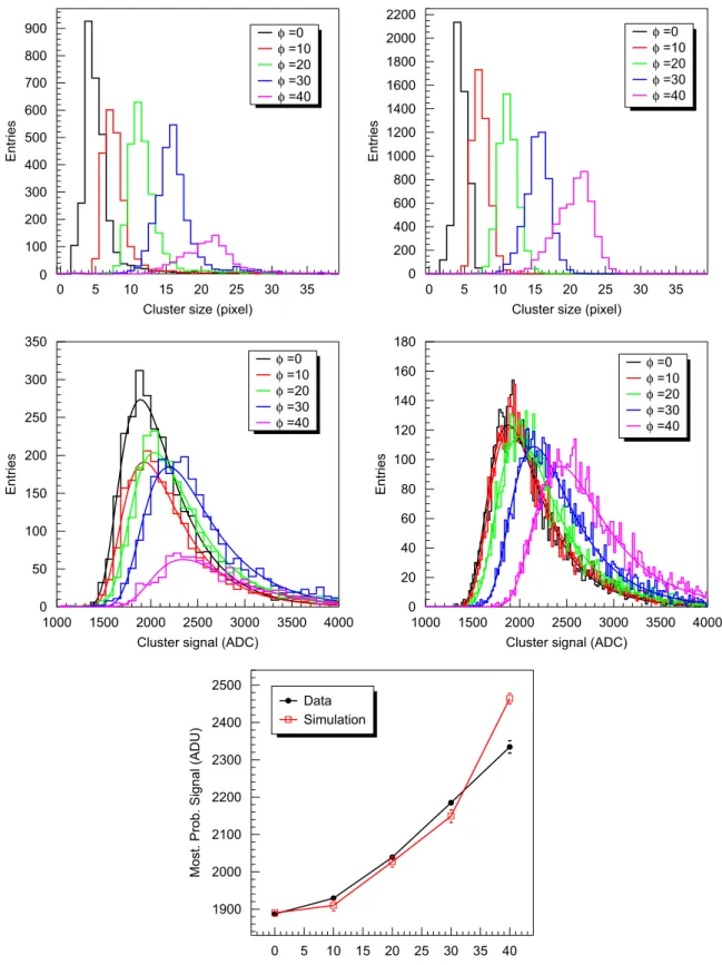
Fig. 4. Comparison between data and simulation. On the left signal and cluster size as a function of the angle of incidence, on the right the corresponding simulation results. Also shown is the most probable signal as a function of the angle of incidence in both data and simulation.
ionizing radiation of the DEPFET has already been demonstrated[4]. The required thinning of the device from 450mm down to 50mm has been successfully performed on test structures [5]. The estimated power consumption is below 5 W, so no active cooling is required[6].
2.1. Testbeam results
About 450mm thick prototype DEPFET modules have been tested in a 6 GeV electron testbeam. The most probable signal is 183574 ADC, the noise 16.4070.01 ADC, yielding aS/N- ratio 112.070.3. The hit positions are reconstructed using the Z-algorithm. This yields a residual width of 8.170.1mm in the X-direction and 7.170.1mm in the Y-direction with 22 36mm2 pixels. The residual width consists of the DEPFET resolution, the intrinsic telescope resolution and a multiple scattering error.1Using a GEANT simulation, the error due to multiple scattering and intrinsic telescope resolution is determined to be 6.94mm[7]. Correcting for this, the DEPFET resolution is 4.2mm in the X-direction and 1.5mm in the Y-direction, better than the 5mm required for the ILC.
In Fig. 2 the efficiency and purity are shown as a function of the seed cut. The efficiency is defined as the ratio of number of clusters found over the number of good tracks. A cluster is accepted when it is within 72 pixels around the predicted position. This yields an efficiency of 99.75% for a 5sseed cut. Most of the missed clusters are missed because the tracks are scattered too much. Applying a very modestw2-cut to remove the worst scattered tracks, the efficiency at a 5s seed cut increases to 99.96%. The purity is defined as the number of clusters that correspond to a track, over all clusters. At a 5sseed cut, the purity is around 97%. Increasing the seed cut to 7s both the efficiency and purity become close to 100%. Note that the most probable signal for seeds is around 60s.
2.2. Zero suppression
It is essential during ILC operation to reduce the data volume. Therefore, zero-suppression capability was im- plemented in the readout chip. In the laboratory, the zero- suppressed readout capability of the DEPFET system was demonstrated using an 247Am-source. InFig. 3the entire DEPFET occupancy is shown as a function of the threshold value in the comparator, clearly displaying that the zero-suppression works and source induced clusters are found. Note that the occupancy is limited by the buffer size, leading to the saturation of the occupancy at 9%.
3. Performance of a DEPFET vertex detector
Besides the R&D on the device, a large (physics) simulation study is underway using a vertex detector consisting of 50mm thick DEPFET sensors. The device
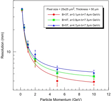
parameters are extracted from the testbeam results. The device is implemented in MOKKA2[8]. The digitization is done using MARLIN[9]; here Landau fluctuations, charge transport, charge sharing and diffusion, the Lorentz shift and electronic noise are simulated. In Fig. 4, testbeam results of the 450mm thick DEPFET are compared with simulation of a 450mm thick DEPFET. The correspon- dence between the testbeam results and the device simulation is excellent. Using the DEPFET parameters extracted from the testbeam results, a simulation of a DEPFET vertex detector consisting of 50mm thick DEPFETs was done. The simulation yields an impact parameter resolution, parametrized bys2¼ab/pTsin3/2y at the ILC in a 3 T magnetic field with a¼3.1mm and b¼7.4mm GeV/c, seeFig. 5,which is better than the ILC requirement ofao5mm and bo10mm.
4. Summary
The DEPFET program is in full swing. Many of the ILC requirements have already been addressed. The DEPFET was tested in a testbeam with 6 GeV/c electrons. The S/N for the 450mm thick detector was found to be larger than 110. The position resolution is smaller than the required 5mm. At a seed cut of 7s, the efficiency and purity are both approximately 100%.
In the readout chip a zero-suppression capability has been implemented. The functionality using a radio-active source was demonstrated. The performance of the zero suppression is currently being tested in a testbeam.
Particle Momentum (GeV)
0 4 10 12
Resolution (mm)
10
Pixel size = 25x25 μm2, Thickness = 50 μm B=3T, a=3.1μm b=7.4μm GeV/c B=4T, a=3.9μm b=7.3μm GeV/c B=5T, a=4.7μm b=7.3μm GeV/c
2 6 8
Fig. 5. Impact parameter resolution as a function of the particle momentum for various magnetic field strengths.
1Note that the multiple scattering error is significant since the beam
consists of 6 GeV/c electrons. 2A GEANT4 package adapted for the ILC.
The predicted performance of a DEPFET based vertex detector, obtained from a simulation where the DEPFET testbeam performance is implemented, is very good.
New large size DEPFET structures are currently being produced. For the final ILC vertex detector, 5124096 pixels DEPFETs are needed. In the current production 512512 and 1284096 pixel devices are being produced.
Currently, the analysis of a high energy testbeam is in progress.
References
[1] T. Behnke et al., A detector for TESLA, TESLA Technical Design Report part IV, DESY 2001-011 ECFA, 2001.
[2] M. Winter, et al., Development of a high precision and swift vertex detector based on cmos sensors for the international linear collider,
DESY Internal Report PRC R&D 01/04 and Update 2(05), May 2005.
[3] J. Kemmer, G. Lutz, Nucl. Instr. and Meth. A 235 (1987) 356.
[4] L. Andricek, P. Fischer, K. Heinzinger, S. Herrmann, D. Herz, M.
Karagounis, et al., The MOS-type DEPFET pixel sensor for the ILC environment, in: Proceedings of the International Workshop on Semiconductor Pixel Detectors for Particles and Imaging-PIXEL 2005, Bonn, September 2005, Nucl. Instr. and Meth. A 565 (2006) 165.
[5] L. Andricek, G. Lutz, M. Reiche, R.H. Richter, IEEE Trans. Nucl.
Sci. NS-51 (3) (2004) 1117–1120.
[6] R. Kohrs, L. Andricek, P. Fischer, M. Haerter, M. Karagounis, H.
Kru¨ger, et al., IEEE Trans. Nucl. Sci NS-52 (4) (2005).
[7] D. Scheirich, Testing semiconductor detectors using beam of charged particles, B.Sc. Thesis, Charles University, Prague 2006, available at /http://www-ucjf.troja.mff.cuni.cz/bsc_theses/bc_scheirich.pdfS. [8] /http://polywww.in2p3.fr/activites/physique/geant4/tesla/www/
mokka/mokka.htmlS.
[9] /http://ilcsoft.desy.de/marlin/S.