DEPFET sensor design using an experimental 3d device simulator
K. G¨artneraand R. H. Richter b,∗
aWIAS, Mohrenstr. 39, 10117 Berlin, Germany, work supported by the HP ’Integrity for Research Program’
bMPI f¨ur Physik, F¨ohringer Ring 6, 80805 Munich, Germany
Abstract
A DEPFET sensor array element with rectangularly shaped channel geometry is simulated and optimized using an experimental three dimensional (3d) device simulator. Due to the relatively large detector volume, the highly refined discretization necessary in MOS channels and the existence of floating potential regions within the DEPFET, the simulation is challenging especially in three dimensions. The results give valuable insight into all operation stages.
Charge collection is in the focus here but also Read and Clear operation of the DEPFET are considered in order to evaluate the response of the device to a signal charge. The results are used to design the next DEPFET prototypes for ILC. The numerical features of the experimental 3d code are briefly discussed.
Key words: DEPFET, Active Pixel Sensor, Vertex Detector, Linear Collider, High Energy Physics PACS:07.77.Ka, 49.40.Wk, 02.60.Cb
1. Introduction
The DEPleted Field Effect Transistor struc- ture, abbreviated DEPFET, provides detection and amplification properties jointly [1]. A MOS or junction field effect transistor is integrated onto a high ohmic detector substrate. By means of sidewards depletion and an n-implant, a potential minimum for electrons is created underneath the transistor channel. This acts as an Internal Gate of the transistor. A particle entering the detector creates electron-hole-pairs in the fully depleted silicon bulk. While the holes drift into the rear contact, the electrons are collected in the Internal Gate where they are stored. The signal charge
∗ Corresponding author. Tel. +49 89 83940043, fax. +49 89 83940013, e-mail rar@hll.mpg.de
leads to a change in the potential of the Internal Gate, resulting in a modulation of the channel current of the transistor. A more detailed descrip- tion of the DEPFET structure and its operation can be found in [1],[2]. The simultaneous detec- tion and amplification feature makes DEPFET pixel detectors very attractive for low noise appli- cations [3],[4]. Due to its high signal to noise ratio at very low power consumption, the DEPFET can also be used on very thin detector substrates, for instance as a vertex detector for the International Linear Collider (ILC) [5]. Based on these inherent features, detector developments for X-ray spec- troscopy [4] and for particle tracking [6],[7],[8] have been started. For space applications the minimum pixel size is defined by imaging properties of the X-ray mirrors. Rather relaxed pixel sizes of about 75µm or larger can be chosen ensuring a large
fraction of events with complete charge collection in one pixel and high energy resolution. DEPFET pixel of this area can be designed with a closed annular channel geometry [4]. For the vertex de- tector at ILC much smaller pixel sizes in the range of 20-30µm will be needed in order to meet the required point resolution of better than 5µm [9].
An open rectangular pixel geometry must be used for layouts of this packaging density. In contrast to standard MOS transistors which are fabricated on low ohmic substrates, the DEPFET contains floating potential regions especially in the clear and insulation regions. This leads to complicated surface potential distributions which influence the movement of the carriers generated in the detec- tor bulk. In this paper the emphasis is placed on the understanding and improvement of the charge collection process.
2. DEPFET Pixel layout for an ILC vertex detector
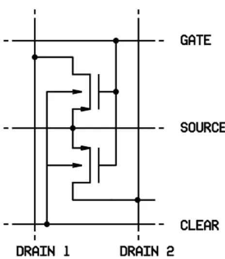
Fig. 1 and Fig. 2 show the circuit diagram and the layout of a double pixel as arranged in an ILC prototype matrix, respectively. Two DEPFET rows are addressed by one set of control lines for the (External) Gates and the Clears of the double row. In this way, one degree of parallelization is im- plemented into the matrix layout. By bisection of the control lines the required row clock rate is re- duced by a factor of two. The number of read out channels doubles of course. Another advantage of a double row addressing is its very compact layout.
Each Drain, Source and Clear region can be shared by two neighboring cells. This symmetry results in an irreducible cell shown in Fig. 2 with Neumann boundary conditions.
In contrast to closed (annular) channel devices the open (rectangular) channel DEPFET needs a lateral insulation structure to suppress any para- sitic lateral currents flowing from Source to Drain.
This task is provided by the first poly silicon layer called Clear Gate which simultaneously defines the potential barrier between the Internal Gate and the Clear region as illustrated in the cross section through the Clear-Clear Gate-Internal Gate in Fig.
Fig. 1. Circuit scheme of an element of an ILC prototype array. Two DEPFET rows are addressed by one set of horizontal control lines.
Fig. 2. Layout of a double cell used for the ILC prototype array. The dashed line marks the simulated region (Cl = Clear).
3. The DEPFET technology available at the MPI Semiconductor Laboratory in Munich is based on direct writing laser photolithography and conven- tional proximity exposure. Both methods allow the fabrication of wafer scale (150mm) detector devices without chip stitching. Since the minimum feature size is about 2µm, the size of crucial defects is in the same order of magnitude. This leads compared with submicron ULSI technologies to a higher fab- rication yield for a given defect density and distri- bution what is even for the production of very large
Metal 2
Metal 1 Poly 2 Poly 1
Clear Gclear Channel
p Deep n n+
Deep p
Fig. 3. Cross section through the Clear - Clear Gate - Internal Gate simulated with DIOS ISE-TCAD [11] (x and y scales inµm).
detectors very important. Nevertheless, the pack- age density is limited by the minimum feature size.
Hence smaller, simpler pixels are a design goal. As shown in [10], it is possible to keep the potential of the Clear Gate at a fixed value during all oper- ation phases. Using this feature reduces the pixel size and the number of row control lines from three to two. It eliminates one of the two control chips (Switcher). The reduction of control and connec- tion effort corresponds to less scattering material and is important for sensor applications in vertex detectors.
3. The experimental 3d code
The main intention writing the code was to study algorithms. Hence the set of models is not large but sufficient to handle the most interesting questions asked in case of this DEPFET design. They are often of the type: is design A better than design B? The simulated doping profiles are of limited precision due to their 2d nature, hence one has at least two reasons to aim on the comparison aspect and to gain qualitative insight.
The classical van Roosbroeck system [12] is solved on a bounded Lipschitzian domain Ω and times 0< t≤T or steady states. It is supposed that Ω admits a conforming Delaunay simplex grid [13].
−∇ ·²∇ψ=f−n+p, (1)
∂n
∂t +∇ ·µnn∇φn=R, (2)
∂p
∂t − ∇ ·µpp∇φp=R, (3) ψ electrostatic potential, n = nieψ−φn, p = nieφp−ψ electron, hole densities, ni intrinsic car- rier density,φn,φpquasi-Fermi-potentials,ttime, R=r(n, p)(n2i−np)+srecombination/generation and ’outer’ (space and time dependent) sources.
The discretization is seen as weak form of the Scharfetter-Gummel scheme [14] and together with an implicit Euler scheme in time it results in a dissipative discrete problem with positive densi- ties [15]. Contact currents are computed by using the properties of the discrete weak formulation and test functions defined by approximate solutions of the adjoint discrete problem (compare [16], too).
Together with Newton’s method (in a positivity preserving form) this allows to compute contact currents fulfilling the balance relation much better than 1010P
j|Ij|<|P
jIj|(Ij current at contact j) for typical distances from the thermal equilib- rium. This is necessary too, to get precise leakage currents at the Back and Clear contacts with mi- nority carrier recombination lifetimes of
τSRH = 0.02sand very reliable Drain current dif- ferences in the order of 1µA in case of a steady state current of a few hundred µA. The current computation is crucial, because it is a primary goal to identify position dependent losses of the generated electrons to the Clear contact.
Solving the linear systems is consuming by far the largest part of the computation time. A block- diagonal preconditioner (singular perturbation theory motivated, a modification of the methods studied in [17]) is combined with cgs [18] to solve the 3x3 systems. The direct solver pardiso ([19],
’google pardiso’) is applied to solve problems with the size of the number of vertices. This reduces the number of factorizations needed roughly to 1 per 100 forward/backward substitutions. This techniques allows problem sizes of order 150000 vertices and the propagation of one electron-hole- cloud can be computed from femto- to microsec- onds during one day using a small SMP machine with 4 CPUs and 8GB memory. The grids used are constructed by the expansion of anisotropic
triangular grids in an orthogonal direction in a preprocessing step. They are treated as general 3d Delaunay simplex grids by the code. The same technique is applied to the 2d ISE-TCAD DIOS doping data [11] to create 3d superpositions of doping profiles. Data given on the first Delaunay simplex grid is interpolated by a fast algorithm onto the nodes of the second one, if they are in the intersection of both grids. The external sources de- scribing the generation of the electron-hole-clouds are of the forms=f(x, y, z)g(t). They are renor- malized to a given number of electrons (holes) to exclude the spatial discretization error in the total generated charge for different generation positions and the very different resolution of the grid. The time integral G = RT
0 g(t) is evaluated twice: at first during the renormalization with very small time steps, this yields a precise approximationG1. Gis approximated a second time during the solu- tion of equations (1 - 3) with larger time steps due to the time step control (G2).G1/G2can be used to correct some time integration errors during post processing.
4. DEPFET operation stages
4.1. Charge collection
In order to avoid charge loss into the clear region the clear is kept at a relatively negative potential VCL of about 1V to 2V during the charge collec- tion stage. The lower limit of the VCL is given by the back emission of electrons from the Clear into the Internal Gate. As mentioned above, the Clear Gate potential VCLG is held on a fixed potential which has to be negative enough to prevent elec- tron back emission and positive enough to suppress a parasitic hole channel in the insulation struc- ture. Depending on technology options, VCLGwas chosen between -2V and 2V to fulfill both require- ments. During charge collection of the DEPFET, the hole channel is switched off, thus the Internal Gate is capacitively coupled to the External Gate and can be shifted to more positive potential by a more positive Gate voltage. During the readout and clear procedures, a hole channel exists and the
Internal Gate is on its minimum potential of about 4V (empty state). For signal electrons generated in the bulk, the Internal Gate has the most attractive potential.
The other floating region within the DEPFET is the Deep p region which shields the n+-Clear from electrons generated in the bulk (Fig. 3). During the Clearthe holes of the Deep p-region are removed by the positively biased n+-contact. Switching back the Clear voltage leads to a slowly changing non steady state in the Deep p region, and the space charge formed by the depleted acceptors acts as a strong potential barrier for electrons duringCol- lection andReading.
4.2. Reading
The figure of merit of the DEPFET is its internal amplification gqgiven in current change per signal charge. The optimum amplification is achieved if the mirror charge of the signal charge is influenced totally in the transistor channel. Due to the In- ternal Gate concept of the DEPFET, only a small fraction of parasitic stray capacitances on the total capacitance of the Internal Gate is involved. How- ever, mirror charges, influenced via any stray ca- pacitance especially to Source and Drain, result in a reduced amplification. The influence of the neg- ative Drain voltage shifts the position of the In- ternal Gate towards the Source and increases the Internal Gate - Source capacitance. A deeper po- sition of the Internal Gate produces a larger frac- tion of stray capacitances. By the simulation of the DEPFET response to a given generated charge, dif- ferent technology and layout options can be evalu- ated w.r.t. gq. Since a field and doping dependent mobility model is not yet implemented in the pro- gram, a constant bulk mobility is assumed. Thus the calculated gqvalues are overestimated but they can fairly be used for comparison based decisions.
4.3. Reset - Clear process
Due to the relative low doping concentration of the Internal Gate which is in the order of several 1016cm−3, it is possible to remove really all elec- trons during the reset (Clear) process. For this
reason the DEPFET can be considered as a detec- tor without reset noise. The clear pulse is applied to the n+ region. The potential barrier formed by the Deep p layer (discussed above) has to be overcome during theClear. If the first poly silicon layer acts as the Clear Gate, the potential barrier between the n+ region and the Internal Gate is clocked during the clear process [4]. In the com- mon Clear Gate approach, which is used here the electrons of the Internal Gate have to overcome the whole Clear Gate region via punch through, which results in a higher but still feasible Clear voltage [10].
Fig. 4. Typical simulation domain: one half of a sin- gle DEPFET pixel designed for ILC (xmax=18µm, ymax=22µm, zmax=50µm, 153700 vertices, 872664 tetra- hedra are used in the final computations).
5. Results
5.1. Charge loss mechanisms
In order to reach the non steady operation state of the DEPFET, at first the voltages represent- ing theClear operation and the MOSFET in the Read state are applied by using the static mode of the 3d solver. Afterwards in a dynamic simula- tion, the Clear voltage is reduced until the Read state is reached, while the the Internal Gate is kept empty. A charge of 1600 electron-hole-pairs is generated within a depth centered around 45µm (z= 5µm) at different (x,y)–positions: North West
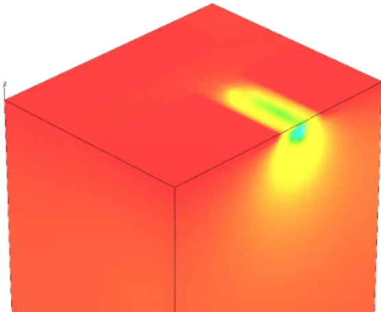
Fig. 5. Electron distribution 10µs after the generation of 1600 electron-hole pairs. Red: clear region (>1019cm−3), yellow: internal gate (≈1016 cm−3), blue: depleted and p-doped regions
Fig. 6. Potential difference in the device as the response to the generation of 1600 electron-hole pairs after 10µs. Red:
no potential change, blue: internal gate changed by about 100mV. (graphics by gltools)
(NW 0 ≤ x≤ 3µm, 19µm ≤y ≤ 22µm), South West (SW 0≤x≤3µm, 0≤y ≤3µm), East (E 15µm≤x≤18µm, 7µm≤y ≤11µm). In addi- tion, the same amount of charge is introduced ho- mogeneously over the entire x-y plane at the same depth in order to detect eventually unidentified po- tential pockets. In order to save computing time, the charge is generated during theRead stage (in-
stead ofCollection) of the DEPFET. This can be considered as a worst case scenario since due to the capacitive coupling of the External Gate, the In- ternal Gate is more attractive for electrons during Collection than duringReading. But on the other hand, the immediate response of the sensor can be monitored during theReadstage only and the time dependence of the charge collection is retrieved, too. An example is shown in Fig. 5. The charge is generated at NW and drifts towards the surface.
Note that a part of the charge reaches the Si/SiO2
interface beneath the Clear Gate above the posi- tion of charge generation (NW). Here, the lateral drift field is negligible, thus the electrons have to reach the Internal Gate by diffusion. The potential change (difference of the potentials calculated after and before charge generation) caused by a signal charge of 1600 electrons generated at NW position is shown in Fig. 6. Despite of the fact that some charge loss is seen at the interface (Fig. 5), the po- tential remains unchanged in this region probably due to the strong capacitive coupling to the Clear Gate over the relatively thin gate oxide. However, the response curves (Fig. 7) show a reduced signal for charges generated in the left region (beneath Clear) at positions NW and SW. The rather slow response time is in the range of severalµs indicat- ing that a part of the charge is collected by diffu- sion. The curve obtained after charge generation at E (directly beneath the Internal Gate) may be considered as a reference for perfect charge collec- tion and response.
5.2. Optimization of charge collection
Long collection times indicate weak lateral drift fields within the pixel. Imperfections in the fabrication process and related potential barri- ers would perturb a diffusion determined charge collection. The charge collection time has to be small compared to the readout time for the entire matrix, approximately 50µs for ILC, else pixels are already read out before their charge collec- tion is completed. Two major changes improved the charge collection. Firstly, an additional non structured n-doped layer was implanted. Beneath the Clear Gate region, the introduced positive
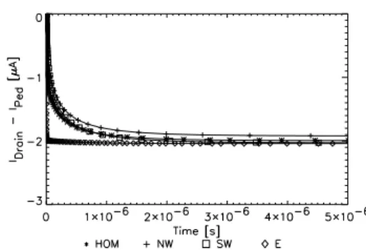
Fig. 7. Current response to 1600 electrons for the de- sign without additional lateral drift field. A pedestal current (IP ed) of 196.2µA was subtracted. Charge is generated at t = 0. Operation conditions during Reading: VClear=2V, VClearGate=1.55V, VDrain=-5V, VSource=0V, VBack=-30V.
space charge shifts the potential minimum from the Si/SiO2 interface to a depth of about 0.7µm.
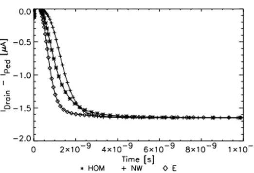
Hence the charge does not drift to the interface but is kept in the potential minimum. In addition, the potential barrier between Clear and Internal Gate is reduced allowing lower voltages for complete Clear. Secondly, lateral drift fields along the Clear Gate region towards the Internal Gate were intro- duced by narrowing the gap between the floating Deep p implant (see Fig. 3) and the p+ Source and Drain regions by 0.5µm. Due to this measure, the potential minimum beneath the Clear Gate drops at the border of neighboring cells by about 0.5V. Both measures result in detector response illustrated in Fig. 8. The charge collection takes a few nanoseconds (note, the different time scales used in Fig. 7 and Fig. 8). The difference in the signal height is due to the different pedestal drain currents resulting in different amplifications.
The improved structure shows no detectable charge losses during the collection process (Fig.
8). This is achieved by the mentioned design and technology changes and by more negative Clear voltages (VClear=1V, VClearGate=-1V).
Fig. 8. Current response to 1600 electrons for the design with additional lateral drift field (IP ed= 91µA). The op- eration voltages are the same as used for the device char- acterized by Fig. 7 apart of Clear voltages which have been changed to VClear=1V, VClearGate=-1V.
6. Conclusions
For the pixel, an open rectangular channel ge- ometry was chosen to design small cell sizes as re- quired for ILC. Making use of symmetry in the layout, an infinite matrix can be simulated by the discretization of an 18µm x 22µm x 50µm half cell.
The current response to charge generated in the de- tector bulk at different positions is used to identify weak spots in the potential distribution causing charge losses and too slow charge collection. Most of the charge generated in the bulk of the silicon is drifting towards the surface and has to be shifted by lateral fields into the Internal Gate. In order to avoid charge loss during diffusion, the poten- tial minimum for electrons is shifted into the depth preventing any charge from reaching the Si/SiO2
interface in the Clear Gate region. This can be achieved by a global deep phosphorus implanta- tion. Efficient lateral drift fields are implemented by minor changes in the layout of the Deep p im- plant. By these measures, the charge loss is sup- pressed at a non detectable level and the charge collection process in the DEPFET array is com- pleted after a few nanoseconds.
Three dimensional device simulation results in es- sential insight into the operation mechanisms of DEPFET arrays. The new experimental code is a stable tool for the simulation of larger detec- tor structures with highly refined subregions, for
instance FET channels. Applying an appropriate grid, the treatment of floating regions (Internal Gate and Deep p) is feasible in static and dynamic modes. Further work is planned to understand and optimize theClearprocess. The results will be used for the design of the next generation of DEPFET prototypes for ILC.
References
[1] J. Kemmer, G. Lutz, New detector concepts, Nucl.
Instr. and Meth. A 253 (1987) 356.
[2] J. Treis et al., Study of noise and spectroscopic performance of DEPMOSFET matrix prototypes for XEUS, Nucl. Instr. and Meth. A, these proceedings.
[3] J. Ulrici et al., Imaging performance of a DEPFET pixel Bioscope system in Tritium autoradiography, Nucl. Instr. and Meth. A 547 (2005) 424.
[4] L. Str¨uder et al., XEUS wide-field imager: first experimental results with the X-ray active pixel sensor DEPFET, in: A. D. Holland (Ed.), High- Energy Detectors in Astronomy, Vol. 5501 of SPIE proceedings, 2003.
[5] L. Andricek et al., Processing of Ultra-Thin Silicon Sensors for Future e+e−Linear Collider Experiments, IEEE Transactions on Nuclear Science 51 (2004) 1117.
[6] R. H. Richter et al., Design and technology of DEPFET pixel sensors for linear collider applications, Nucl.
Instr. and Meth. A 511 (2003) 250.
[7] M. Trimpl et al., A fast read out using switched current techniques for a DEPFET pixel based vertex detector at TESLA, Nucl. Instr. and Meth. A 511 (2003) 257.
[8] M. Trimpl et al., Performance of a DEPFET pixel system for the ILC vertex detector, Nucl. Instr. and Meth. A, these proceedings.
[9] T. Behnke, S. Bertolucci, R.D. Heuer, R. Settles, TESLA: The superconducting electron positron linear collider with an integrated X-ray laser laboratory.
Technical design report. Part IV: A detector for TESLA, V0l. 2b, DESY-01-011, 2001.
[10] C. Sandow et al., Characterization of the clear- mechanism of linear DEPFET-pixel structures, Nucl.
Instr. and Meth. A, these proceedings.
[11] ISE TCAD Release 7.0, V0l. 2b, DIOS, 2001.
[12] W. van Roosbroeck, Theory of flow of electrons and holes in germanium and other semiconductors, Bell syst. Tech. J. 29 (1950) 560.
[13] B. Delaunay, Sur La Sph´ere Vide, Izvestia Akademii Nauk SSSR. Otd. Matem. i Estestv. Nauk 7(6) (1934) 793.
[14] D. L. Scharfetter and H. K. Gummel, Large–signal analysis of a silicon read diode oscillator, IEEE Trans.
Electr. Dev. 16 (1969) 64.
[15] H. Gajewski, K. G¨artner, On the discretization of van Roosbroeck’s equations with magnetic field, ZAMM 76 (1996) 247.
[16] P. D. Yoder, K. G¨artner, U. Krumbein, W. Fichtner, Optimized Terminal Current Calculation for Monte Carlo Device Simulation, IEEE Transactions on Computer Aided Design of Integrated Circuits and Systems 16 (1997) 1082.
[17] H. Gajewski, K. G¨artner, On the iterative solution of van Roosbroeck’s equations, ZAMM 72 (1992) 19.
[18] P. Sonneveld, CGS, a fast Lanczos-type solver for nonsymmetric linear systems, SIAMJ Sci. Stat.
Comput 10 (1989) 36.
[19] O. Schenk, K. G¨artner, W. Fichtner, Efficient sparse LU factorization with left-right looking strategy on shared memory multiprocessors, BIT 40 (2000) 158.
![Fig. 3. Cross section through the Clear - Clear Gate - -Internal Gate simulated with DIOS ISE-TCAD [11] (x and y scales in µm).](https://thumb-eu.123doks.com/thumbv2/1library_info/4006229.1540859/3.892.133.422.133.341/cross-section-clear-clear-gate-internal-simulated-scales.webp)