Clear-performance of linear DEPFET devices
C. Sandow
a,∗ , L.Andricek
c, P.Fischer
b, R.Kohrs
a, H.Kr¨ uger
a, G.Lutz
c, H.G.Moser
c, L.Reuen
a, R.H.Richter
c, L.Str¨ uder
c, J.Treis
cM.Trimpl
a, N.Wermes
a,
a
Physikalisches Institut der Universit¨ at Bonn, Nussallee 12, D-53115 Bonn, Germany
b
Institut f¨ ur technische Informatik, B6, 26, D-68131 Mannheim, Germany
c
MPI Halbleiterlabor, Otto-Hahn-Ring 6, D-81739 M¨ unchen, Germany
Abstract
The proposal of a vertex detector for the International Linear Collider (ILC) using DEPleted Field Effect Transistor (DEPFET) detectors [1] states challenging requirements for the readout electronics and the sensor itself. In contrast to hybrid pixel technologies, DEPFET sensors integrate a first amplification stage in the detector. As the signal readout is non-destructive, the DEPFET requires a reset(clear) mechanism. Optimization of the clear mechanism addressing radiation hardness and timing are presented. Furthermore, the minimal duration for a clear process resulting in a readout free of reset noise will be shown to satisfy the timing requirements of the DEPFET-ILC readout scheme.
Key words: DEPFET, monolithic active pixel sensors, integrated amplification, reset process, Linear Collider, ILC
1. Introduction
The physics of the International Linear Collider (ILC) will be complementary to that of the Large Hadron Collider (LHC). The LHC and its exper- iments have a great discovery potential for new physics, whereas the ILC mainly covers precision measurements on potential new particles and inter- actions. A vertex detector for the ILC has to meet many challenging requirements [2] concerning tim- ing, material budget, spatial resolution and power consumption. The present concept of a DEPFET
∗ Corresponding author: Christian Sandow, Physikalisches Institut, Nussallee 12, 53115 Bonn, Germany; tel. +49-228- 73-2499; fax. +49-228-73-3220.
Email address: sandow@physik.uni-bonn.de (C.
Sandow).
based vertex detector for the ILC [1] can satisfy all the requirements for an ILC vertex detector. Thus, the concept itself transforms those requirements into needs for the detector and its readout system.
In 2003 a dedicated DEPFET-pixel design for
the ILC application has been realized [3]. It fea-
tures small (25µm x 35µm) linear pixels and has
been produced using a newly developed two metal
layer process in the Semiconductor laboratory in
munich. Furthermore, a prototype of the readout
system has been developed [4] and the full system
passed a first beam test in February 2005.
2. DEPFET principle
DEPFET sensors combine a fully depleted sub- strate with a first amplification stage in form of a field effect transistor [5] (see Fig. 1). Underneath the transistor channel a potential minimum, the internal gate, is formed by means of sidewards de- pletion. Additionally a deep-n implantation defines the potential of the internal gate laterally. Imping- ing particles create electron-hole pairs. While holes drift to the backside contact, the electrons are ac- cumulated in the internal gate. Due to the capac- itive coupling of the internal gate to the transis- tor channel, its conductance is controlled by the internal gate’s potential. Therefore the change in transistor current ∆I
Dinduced by the change in charge ∆Q in the internal gate is a measure of the device’s amplification g
Q:
g
Q= ∆I
D∆Q
Present linear devices show a g
Qbetween 240 pA/e
−and 300 pA/e
−[6]. The small capaci- tance of the internal gate (in the order of few fF), which acts as input node of the amplifier, results in very low noise figures of ENC=9.8 e
−at room temperature [8].
As the readout is non-destructive, the electrons have to be removed from the internal gate. Ap- plying a high positive clear-voltage U(Clear on) ≈ 15V to adjacent clear contacts empties the internal gate. Clear ’on’ denotes the state during the clear and Clear ’off’ during charge collection.
3. Requirements for the clear process The concept of a DEPFET based vertex detec- tor for the International Linear Collider states two principal requirements for the clear process:
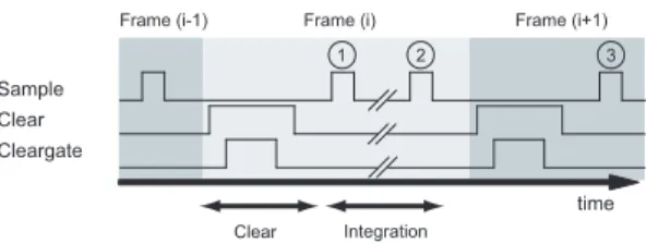
– Complete clear
The proposed readout scheme employing Fast Correlated Double Sampling (CDS) (Fig. 2) ne- cessitates a complete clear. For Correlated Dou- ble Sampling, the drain current is sampled twice within one frame . Immediately after clearing the pixel, the pedestal current is sampled (see
- backside contact deep n
internal gate
Cross section see Fig. 3
Fig. 1. Schematic view of a DEPFET pixel.
Cleargate Clear Sample
time
Frame (i-1) Frame (i) Frame (i+1)
Clear Integration
1 2 3
Fig. 2. Fast Correlated Double Sampling and typical clear- ing scheme.
Fig. 2, sample (1)). After some time of integra-
tion, for the foreseen ILC mode of operation in
the order of 50 µs, the sum of the signal and the
pedestal current is measured (sample (2)). To
obtain the signal current, the pedestal current
has to be stored and afterwards subtracted from
the second sample (2)-(1). Complete clear means
that every reset results in the same pedestal
current. Therefore the DEPFET device is in-
trinsically free of reset noise. As complete clear
has already been shown [7][8] another readout-
scheme is favored. Every reset yields the same
pedestal current, therefore it is possible to sub-
tract the pedestal current measured in the sub-
sequent frame instead of the sample in the orig-
inal frame((3)-(2)), thus resulting in the same
signal current. This sampling scheme makes a
row-wise operation possible, without storing an
entire data-frame during the CDS.
– Fast clear
Another stringent requirement concerns the du- ration of the clear pulse. The proposed row-rate of several ten MHz implies that the CDS includ- ing one clear in between the two samples can be completed in less than 15 ns.
Furthermore, there are some favored properties that could simplify the readout.
– Low clear-voltages
The appropriate clear-voltage swing up to 20 V is supplied by the steering chip SWITCHER II [9]. This chip has been produced using the 0.8 µm AMS high-voltage process which probably gives rise to problems with radiation tolerance.
If the clear-voltage swing could be lowered, the steering chip can be produced using a reduced structure-size which will yield in improved radi- ation hardness.
– Static cleargate operation
As pointed out below, up to now the prototype’s clearing scheme includes the clocking of an ad- ditional MOS-structure, the cleargate. This of- fers full control of the clear process during pro- totype development. If complete clear is achiev- able with a static cleargate potential, the ad- ditional clocked signal becomes obsolete, which will improve the timing scheme for the clear, as no timing substructure of the clear is needed.
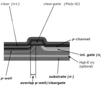
4. A deeper look into the clear process As the clear process is one of the crucial points for the ILC application of DEPFET devices, the underlying mechanisms will now be presented in more detail (cf. Fig. 3). In order to avoid charge loss into the clear n
+-implantation during charge collection, the clear is shielded by a deep p-well implantation. For this implantation gives rise to a potential barrier, the process of clearing becomes more difficult. In order to control this potential barrier and the potential of the substrate neigh- boring the internal gate, a cleargate-structure has been introduced (see Fig. 1). In the prototype op- eration mode, the cleargate is clocked in order to ease the clear process. During charge collection, the
cleargate has to be kept on a low potential because of possible charge loss underneath the cleargate.
The typical timing scheme consists of a longer clear-pulse and a shorter cleargate-pulse which is embedded in the clear-pulse duration (Fig. 2). If both, clear and cleargate are switched to upper po- tential, two mechanisms contribute to the removal of the electrons from the internal gate.
First, the positive cleargate gives rise to a n - channel in the p-well connecting internal gate and clear. Second, the potential of the clear can reach- through the p-well potential barrier via punch- through. But whereas the n-channel is situated at the surface, the punch-through is also effective in the depths of the internal gate. When applying the appropriate voltages, no electrons will be left in the internal gate after a very short time. Now low- ering the cleargate potential, some electrons which might have remained underneath the cleargate are moved into the clear via punch-through, prevent- ing them from flowing back into the internal gate.
This effect occurs, if the clear-pulse does not em- bed the cleargate-pulse. Finally, all electrons are successfully removed and the clear potential can be lowered, again.
5. Optimizing the DEPFET device
5.1. Geometry of the cleargate region
The performance of the clear strongly depends
on the geometry of the cleargate region. In order
to optimize the cleargate geometry, a number of
device simulations have been performed. Several
single pixel test-structures with varying length of
the cleargate (L CG) and different overlap between
cleargate and p-well (L CG DP) have been pro-
duced. It is expected that with increasing overlap
(L CG DP) the clear-voltage needed for complete
clear increases as the potential barrier widens. The
overall length of the cleargate (L CG) alters the ca-
pacitive coupling of the cleargate’s potential to the
substrate and the p-well, thus easing the punch-
through if the cleargate length is reduced. So op-
timizing the cleargate geometry is a key to low
clear- and cleargate-voltage swings, while main-
Fig. 3. Cross section of the cleargate region as marked by the line in Fig. 1.
tainign the full clearing capability.
5.2. High-Energy Implantation
Another possible solution to decrease the cleargate-voltage swing is the introduction of an additional implantation. A high energy n
+- implantation in the depth of 1.2 µm moves the internal gate 0.4µm down to a depth of 1.0 µm underneath the surface. As the electrons now flow deeper in the substrate, the punch-through be- comes easier because in that depth, the p-well’s capacitive coupling to the cleargate is reduced.
This results in a lower cleargate-voltage swing, thus enabling static cleargate operation. Another effect is a reduced g
Q≈240 pA/e
−due to reduced capacitive coupling of the internal gate to the p-channel.
6. Principle of the Measurements
In order to verify the above statements by measurements, the completeness of the clear de- pending on the clear and cleargate-voltages has been studied. The basic idea is to use the absence of reset noise as a proof of complete clear. If the clear is complete, every clear process yields the
same pedestal current. Thus the pedestal spread contribution due to reset noise vanishes. Then, the system noise only determines the pedestal spread.
In order to measure the pedestal spread, approx- imately 30.000 electron-hole-pairs have been gen- erated in the substrate by using a pulsed infrared Laser (λ=808nm, ∆t
pulse=12ns). The electrons are collected in the internal gate during an inte- gration time of 2,9 µs. Then a clear-pulse was ap- plied and afterwards, the pedestal current I
pedhas been measured using a discrete transimpedance- amplifier and an ADC. This process was repeated up to 100.000 times. If there was no noise of the readout-electronics, the pedestal spread would be equal to the reset noise. As the noise contributions of the readout electronics and the reset noise add quadratically, a global minimum of the pedestal spread corresponds to vanishing reset-noise and therefore to complete clear. The absolute minimal value equals the system noise. Such a measure- ment of the pedestal spread has been repeated for up to 2500 different clear and cleargate-voltage combinations.
7. Results
7.1. Low clear-voltages and static cleargate operation
The first focus of measurements is the influence
of the pixel geometry on the clear process. There-
fore, single pixel test-structures with a pixel-size
of 25x35µm
2and different clear geometries have
been tested. The duration of the clear pulse was
208 ns with a 125 ns embedded cleargate pulse and
a rise time in the order of 15 ns. U(Clear off)=3V
and U(Cleargate off)=0V have been chosen such
that charge losses are minimized. Figure 4 shows
the dependence of the pedestal current spread as
a function of U(Clear on) and U(Cleargate on)
for a typical clear geometry. The noise given by
the pedestal spread, σ, is measured in nA as the
DEPFET returns a current. Complete clear can be
obtained for U(Clear on) > 13V and U(Cleargate
on) > 4V. Figure 5 shows the same measurement
on a pixel with a shorter cleargate (reduced L CG).
6 8 10 12 14 16 18 0
1 2 3 4 5 6
(noise)
[nA]
U (Clear on) [V]
U (Cleargate on) [V]
0
15
30
45
60
75
90
100 Complete
Clear
Fig. 4. Pedestal spread for a single pixel without High-E implantation L CG=7.2µm, L CG DP=1.5µm, U(Clear off)=3V, U (Cleargate off)=0V.
6 8 10 12 14 16 18
0 1 2 3 4 5 6
Complete
Clear
U (Clear on) [V]
U(Cleargateon)[V]
(noise)
[nA]
0
15
30
45
60
75
90
100
Fig. 5. Pedestal spread for a single pixel without High-E implantation L CG=4.2µm, L CG DP=1.5µm, U(Clear off)=3V, U (Cleargate off)=0V.
As stated above, with less L CG complete clear can also be achieved with lower U(Cleargate on) ≈ 0V at the drawback of higher U(Clear on) ≈ 16V.
With U(Cleargate off)=0V, this geometry offers static cleargate operation, but nevertheless a clear- voltage swing of 13V is not satisfactory. Figure 6 shows a pixel with reduced overlap between clear- gate and p-well. In this case the voltages needed for complete clear can be reduced to U(Clear on) ≈ 6V, U(Cleargate on) ≈ 4V, thus resulting in a re- duced clear-voltage swing of 3V. Because there are
6 8 10 12 14 16 18
0 1 2 3 4 5 6
Complete
Clear Complete
Clear
(noise)
[nA]
U (Clear on) [V]
U(Cleargateon)[V]
0
15
30
45
60
75
90
100
Fig. 6. Pedestal spread for a single pixel without High-E implantation L CG=6.2µm, L CG DP=0.5µm, U(Clear off)=3V, U (Cleargate off)=0V.
no test pixels with small L CG and small L DP CG as well, it is impossible to check wether small clear- voltage swing and static cleargate operation can be obtained at the same time only due to variations of the pixel geometry.
The increase of the noise for high U(Clear on) as seen in Figures 4 and 6 can be identified as an artifact due to the single pixel form of the test- structures. A high U(Clear on) attracts leakage- current electrons from the surrounding substrate which are subsequently collected in the internal gate after the clear potential is lowered.
An additional High-Energy implantation mainly effects the U(Cleargate on) needed for complete clear. Because the structures with High-E offer sta- tic cleargate operation, small matrices of 4x8 Pix- els with a pixel-size of 24x36 µm have been pro- duced which posess a common cleargate contact for all pixels. Its pixel geometry is: L CG=6.2 µm, L DP CG=1.7µm. Fig. 7 shows the dependence of the pedestal current variations on U(Clear on) and U(Cleargate), which is operated in a static mode.
Complete clear can be observed for U(Clear on)
> 8V and U(Cleargate) > -1V. In contrast to sin-
gle pixels without High-E, U(Cleargate)=0V dur-
ing charge collections does not correspond to min-
imal charge losses. Only at U(Cleargate)=-2V the
maximum charge collection is assured. To achieve
6 8 10 12 14 16 18 -4
-3 -2 -1 0 1 2 3
U (Clear on) [V]
U(Cleargate)[V]
0
15
30
45
60
75
90
100 (noise)
[nA]
Complete Clear
Fig. 7. Pedestal spread for a pixel within a small ma- trix with High-E implantation and static cleargate oper- ation. L CG=6.2µm, L CG DP=1.7µm, U(Clear off)=3V, U (Cleargate off)=-2V.
complete clear at this cleargate potential, U(Clear on) has to be raised to 12V, thus enabling static cleargate operation.
7.2. Fast Clear
All results presented above have been measured using a width of the clear pulse of ∆
t(Clear)=208ns.
The DEPFET-ILC-concept relies on a fast clear with ∆
t(Clear)<20ns. Fig. 8 shows the depen- dence of the pedestal current variations on the clear pulse duration. These measurements have been performed on the small matrix with High- E already known from Figure 7 and with static cleargate. In contrast to the measurements pre- sented so far, the clear-pulse was generated by a fast pulse-generator with a rise time of 2 ns.
At U(Clear on)=14V where complete clear with
∆
t(Clear)=208ns has been achieved, the com- pleteness of the clear is independent of the pulse duration. This means, that complete clear can be achieved for 10 ns pulse duration, which is short enough for the ILC readout scheme. For clear- voltages U(Clear on)=10V and U(Clear on)=8V which only result in an incomplete clear, the clear performance deteriorates for shorter clear pulses.
0 20 40 60 80 100 120 140 160 180 200 220
14 15 16 17 18 19 20 21 22
14 15 16 17 18 19 20 21 22
U Clear on
= 8V
U Clear on
= 10V
U Clear on
= 14V
(noise)[nA]
t (Clear) [ns]