Technische Universität München Fakultät für Physik
Max-Planck-Institut für Physik (Werner-Heisenberg-Institut)
Master Thesis
Influence of the Metallization on the Charge Collection Efficiency of
Segmented Germanium Detectors
Einfluss der Metallisierung auf die Ladungssammlungseffizienz von segmentierten Germaniumdetektoren
Lukas Hauertmann
March 30, 2017
Supervisor: Dr. I. Abt
Contents
Introduction and Motivation 1
1. Germanium Detectors 3
1.1. Semiconductor Detectors . . . 3
1.1.1. Band Structure in Crystals . . . 3
1.1.2. Impurities and Doping . . . 4
1.1.3. p-n Junction, Diode . . . 5
1.1.4. Detectors . . . 6
1.1.5. Electrodes and Metallization . . . 6
1.1.6. Signal Creation . . . 7
1.2. Siegfried III . . . 8
1.2.1. Electrical Field . . . 9
1.2.2. Surface Map . . . 10
2. GALATEA 13 2.1. General Setup . . . 13
2.1.1. Vacuum and Cooling . . . 13
2.1.2. Mechanics . . . 15
2.2. Hat Positioning System - HPS . . . 16
2.3. Read-out Electronics . . . 18
3. Data Taking 19 3.1. Background Radiation . . . 19
3.2. Uncollimated Thorium-228 Source . . . 19
3.3. Collimated Americium-241 Source . . . 21
3.3.1. Size of the Beam Spot . . . 22
4. Data Acquisition and Processing 23 4.1. Data Acquisition System (DAQ) . . . 23
4.2. Pulse Preprocessing . . . 23
4.2.1. Baseline Correction . . . 24
4.2.2. Decay Correction . . . 24
4.3. Measured Pulse Amplitudes . . . 25
4.4. Cross-talk and Amplifications . . . 26
4.5. Reconstruction of the Energies . . . 27
4.5.1. Core Energy . . . 27
4.5.2. Segment Energies . . . 28
4.6. Crosscheck of the Energy Reconstruction Procedure . . . 31
5. Detector Positioning 35 5.1. Location of Segment Boundaries . . . 35
5.2. Location of Crystal Axes . . . 38
5.2.1. Determination of Rise Times . . . 38
5.2.2. Determination of the Location of the Crystal Axes . . . 39
6. Detector Characterization with Respect to Metallization 41 6.1. Observed Energy for Alpha Radiation . . . 41
6.2. Count Rates and Beam Spot . . . 43
6.2.1. 59.5 keV Gammas . . . 43
6.2.2. Alpha Particles . . . 44
6.3. Width of Peaks . . . 49
6.3.1. Gamma Peaks . . . 49
6.3.2. Alpha Peaks . . . 49
6.4. Continuum to Peak Ratios . . . 50
6.5. Charge Trapping and Truncated Mirror Pulses . . . 52
6.6. Rise Times . . . 56
Summary and Outlook 59
A. Screws - N-470.V PiezoMike Linearaktors 61
B. Tau Decay Constants τi of the pre-amplifiers 63
Introduction and Motivation
Radiation and particle detectors are of great importance in industry, medicine and science.
In industry and medicine, they are often used together with radioactivity introduced into the system under investigation. For example, the flux inside pipes can be analyzed, the mixture of gases or liquids inside closed containers can be determined and fill levels can be measured. The search for fractures in solid bodies is another application. In medicine, they are mainly used to look into the human body, identify injuries and tumors, and monitor radiation therapy. In particle physics, they are used to locate and identify particles produced by colliders, by cosmic radiation and by radioactive decays.
Complex assemblies of thousands of detectors are needed to make discoveries like the ob- servation of neutrino oscillations and the recent discovery of the Higgs boson. Radia- tion detectors are also used to search for new physics like neutrinoless double beta decay (0νββ) [1] and the scattering of dark matter off ordinary matter [2]. Such searches require an extremely low background. Germanium detectors, which are the subject of this thesis is focused, are a preferred technology for such so-called low-background physics.
The GERmanium Detector Array (GERDA)[3] is the currently leading germanium based experiment searching for neutrinoless double beta decay of 76Ge:
A
ZX→Z+2AX + 2e− . (0.1)
The reduction of the background was the biggest challenge for GERDA and will be for future projects. So far, 0νββ has not been observed and the expected event numbers are very small. Therefore, the germanium detectors themselves have to be extremely well understood. They act as source and detector. The energy expected to be observed from the two electrons emitted in 0νββ is equal to the energy released in the decay. The excellent energy resolution of germanium detectors makes it possible to distinguish 0νββ from the standard neutrino accompanied double beta decay where part of the energy is carried away by the two neutrinos.
The observation of 0νββ would reveal a lot about neutrinos. Foremost, it would prove that they are Majorana and not Dirac particles. This would mean that they are their own antiparticles. In addition, it would give information about the effective neutrino massmee. If 0νββ is not observed above a level corresponding to mee ≈ 10 meV, an inverted mass hierarchy within the framework of Majorana neutrinos is excluded. However, 0νββ might also occur through new physic mechanisms, with other particles than neutrinos exchanged.
Different isotopes are used to search for 0νββ. The main focus is on 76Ge and 136Xe [4].
Xenon can also be used as source and detector, both in the liquid and the gaseous phase.
Germanium detectors are compact and have a better energy resolution compared to gaseous or liquid detectors. However, individual detectors have limited mass and they have to be operated at cryogenic temperatures. They are semiconductor detectors where radiation deposits its energy inside the germanium by creating electron-hole pairs. The positive and negative charge carriers are separated by an external electrical field and collected at
electrodes on the surface of the detector. The surface of germanium detectors is usually metallized to stabilize the electrical field and assure a good charge collection efficiency.
In this thesis, results on the influence of the metallization are presented. The true-coaxial n-type germanium detector Siegfried III with partially and fully metallized segments was irradiated with alpha particles and low energy photons from an Americium-241 source.
Alphas penetrate the detector only a few microns and deposit all their energy in extreme proximity to the surface. Low energy photons penetrate a few millimeters and probe a different volume than the alphas. Thus, any effects due to missing metallization can be studied directly at the surface and in the volume underneath.
The measurements were performed in the test facility GALATEA (GermAnium LAser TEst Apperatus) at the Max Planck Institute for Physics in Munich. The test stand mechanics was upgraded to perform the surface scans presented.
The thesis is structured in the following way:
Chapter 1: The functionality of germanium detectors in general is described. The special germanium detector Siegfried III with different types of segment metallization is introduced.
Chapter 2: The experimental setup GALATEA is introduced. The focus is on an upgrade of the mechanics, i.e. the hat positioning system (HPS), which made safe rotational scans of the detector possible.
Chapter 3: Natural background radiation as well as sources based on the isotopes 241Am and 228Th are described. The scans performed to study the detector are introduced.
Chapter 4: The data acquisition system and the pulse preprocessing-procedure are de- scribed. In addition, improvements to the cross-talk correction and calibration procedure are explained and verified.
Chapter 5: The determination of the detector position and orientation with data is pre- sented. The exact position of the detector is important for further detailed studies.
Chapter 6: The analysis of the data with respect to the metallization is presented. The analysis concentrates on events induced by alpha particles and photons from the 241Am source, which was used to illuminate different spots on the detector surface. It includes investigations of the energy response, the resolution, the charge collection efficiency and the rise times of the charge pulses.
1. Germanium Detectors
1.1. Semiconductor Detectors
Germanium is a semiconductor similar to silicon. There is a wide range of literature about semiconductors and semiconductor detectors, e.g. [5, 6], in which the subject is discussed in detail. Here, a brief summary is given.
1.1.1. Band Structure in Crystals
Semiconductors are solids with a crystalline structure. The periodic structure of the atoms in crystals results in a band structure of the allowed energy states of the electrons. There are two main bands, the valence band and conduction band. The electrons inside the valence band are bound to atoms or are part of covalent bonds and don’t contribute to the electrical conductivity of the material. In contrast, electrons inside the conduction band are free to move inside the material. However, not only these excited electrons are responsible for the conductivity. When an electron is excited, a vacancy in the valence band is created.
This "hole" can be seen as a positive charge, which also contributes to the conductivity.
Therefore, one often speaks of "electron-hole pairs".
The concept of band structure allow a separation of crystalline materials into three groups:
conductors, semiconductors and insulators. The key quantity of this separation is the bandgap, Eg. This is the energy difference between the highest state of the valence band and the lowest state of the conduction band. Figure 1.1 illustrates the differences between the band structures of these three groups. In absence of any excitation, all electrons of
Figure 1.1.: Simplified illustration of the difference between the band structures of insula- tors, semiconductors and conductors. The key quantity is the bandgap Eg. the material are in the valence band, which is completely filled, while the conduction band is completely empty. Hence, the electrical conductivity is zero. In reality, with finite temperatures, thermal excitations lift electrons from the valence band to the conduction band, resulting in a finite conductivity.
Equation 1.1 gives the probability per unit time that an electron-hole pair is created by thermal excitation, where T is the absolute temperature, kB the Boltzmann constant and C is a characteristic constant of the material.
p(T) =CT3/2exp− Eg 2kBT
(1.1)
The probability strongly (exponential) depends on Eg. For larger bandgaps, like in insu- lators, the probability is close to zero, resulting in a high electrical resistance. Insulators usually have Eg >5 eV, whereas for semiconductors Eg ≈1 eV. Without an external elec- tric field, any electron-hole pairs recombine after some time and an equilibrium develops.
Therefore, a finite concentration of free charge carriers is present for a given temperature.
The bandgap of germanium is 0.665 eV and for silicon 1.115 eV, both at 300 K [6]. In con- trast to silicon detectors, germanium detectors cannot be operated at room temperatures due to their small bandgap. The free charge carrier density is too high to allow for a working diode. Therefore, they must be cooled down to liquid nitrogen temperatures (T<100 K).
In addition, germanium detectors cannot be operated in air, since water would condensate on the detector surface.
1.1.2. Impurities and Doping
Perfect crystals without impurities or vacancies do not exist. In reality, the impurities strongly influence the electrical properties, because they add allowed energy states for the electrons between the valence and the conduction band. These states make it easier to lift electrons into higher states and create free charge carriers, because the required energy is decreased. This can be used to engineer the electrical properties by intentional adding impurities, so-called doping. There are two possibilities: n-type and p-type doping.
In case of n-type doping, atoms of an element with one more valence electron than the intrinsic element are added into the crystal lattice. Since there are still far more intrinsic atoms, the lattice remains in its previous structure. Thus, the extra electron of the dopant is just lightly bound to the added atom, since it isn’t part of any covalent bond. Therefore, only a small amount of energy is needed to lift this electron into the conduction band.
These added atoms are called donors, since they donate their extra electron. In the picture of bands, they create allowed energy states closely beneath the conduction band. Thermal excitation is therefore enough to lift nearly all those extra electrons into the conduction band.
In case of p-type doping, atoms of an element with one less valence electron are added.
These are called acceptors. In the band picture, they create energy states just above the valence band. Thus, not all states in the valence band are filled.
In both cases, charge neutrality is conserved. In n-type semiconductors the free electrons in the conduction band are responsible for the electrical conductivity and the holes are fixed (positive space charges). In p-type semiconductors it is the other way around. The holes in the valence band are responsible for the conductivity and the electrons are fixed at the locations of the acceptors (negative space charges).
1.1. Semiconductor Detectors
1.1.3. p-n Junction, Diode
The bulk, the body, of a crystal is either p-type or n-type. A p-n-junction, diode, is formed by creating a thin layer of n-type or p-type material, respectively. A simple p-n junction and its electrodynamics are illustrated in Fig. 1.2. The free charge carriers of
Figure 1.2.: Illustration of the electrodynamics of a p-n junction. On the left, the differently doped areas in a crystal are shown. Towards the right, the resulting fixed space charge density, ρ(x), the electric potential, ϕ(x), and the electric field strength,E(x), are shown. The positive and negative charges in the doped areas represent the free charge carriers (holes in the valence band and electrons in the conduction band). The contact potential, VC, is the difference of the potential between the ends of the depletion region, with depth d, over which the space charge density extends, see text.
either charge diffuse to regions where their concentration is lower. Hence, electrons (holes) diffuse from the n-type (p-type) to the p-type (n-type) region, where they recombine with holes (electrons). This results in a fixed positive space charge in the n-type region and a fixed negative space charge in the p-type region. The fixed space charge density, ρ(x), creates an electric potential,ϕ(x), and an electric field, E(x),
d2ϕ
dx2 =−ρ(x)
(1.2) , E(x) = −dϕ
dx (1.3) , where is the dielectric constant of the medium.
The electric field ends the diffusion when an equilibrium is reached. The region over which ρ(x) extends has no free charge carriers inside and is called the depletion region with the depth, d. The doping concentrations determine d. If the p-type doping concentration is higher than the n-type doping, it penetrates deeper into the n-type than into the p-type.
Thus, the doping concentration of the thin layer must be of much higher concentration, than the bulk, in order to deplete the bulk completely. The difference in potential at the two ends of the depletion region is called the contact potential VC and is of the order of magnitude ofEg (divided by the elementary charge).
1.1.4. Detectors
A p-n junction without biasing could serve as a detector, but, for most applications, would have very poor properties. The depleted region would be small and hence, the efficiency of detecting certain particles (e.g. photons) would be small too. In addition, many of the created electrons and holes would get trapped on the way to the collecting electrodes, since the electric field would not be strong (VC ≈1 V) and the velocity of electrons and holes is proportional to the electric field.
Therefore, an external field is applied to increase the depletion region and the electric field strength. A positive potential is applied to the side with n-type doping. This results in a reverse bias, which closes the diode. Any current observed is called a leakage current.
The depth d can be approximated as
d≈
s2VB
eN =q2VBµe,hρb (1.4)
whereis the dielectric constant of the medium,VB (B for biased) is the externally applied voltage, e is the elementary charge, N is the doping concentration of the bulk, µe,h is the electron or hole mobility, depending on the doping type of the bulk, and ρb is the electrical resistivity of the bulk. If the bulk of a detector is n-type (p-type) the detector is referred to as an n-type (p-type) detector.
Equation 1.4 shows that d is proportional to √
ρb. This resistivity can be increased by using high-purity materials. Germanium can be produced to a much higher purity than silicon. That is why it is possible to build detectors with d of the order of centimeters out of germanium, but not out of silicon.
High-purity germanium (HPGe) detectors have typical impurity levels of 10−10cm−3, thus voltages of a few kV can establish depletion depths of several centimeters. Such large crystals of high purity are pulled via the Czochralski-method [7].
1.1.5. Electrodes and Metallization
To apply the bias voltage equally over the hole detector, both surfaces of the detector must provide a well defined potential. Since the doping concentration of the thin layer is much higher than the doping concentration of the bulk, the thin layer isn’t depleted completely and its surface is therefore conductive and of equal potential. This area is referred to as the p+-contact/-electrode. On the other side of the detector, a depletion of the surface is prevented by increasing the doping concentration at this surface. Thus, also this surface is conductive and of equal potential. This conductive area is referred to as the n+-contact/- electrode. In both contacts the electrical field is zero. The different areas and the net doping concentration, Nnet, are illustrated in Fig. 1.3 for an n-type detector. In germanium detectors, the n+-contact is usually done through a lithium drift and the p-type layer is usually done through boron implantation. Then+-contact is about a millimeter thick while the boron implant is just a few micrometer thick. Both are, however, much thinner than the bulk. Since there is no electrical field inside these layers, they are also called "dead layers". In dead areas, the electron-hole pairs won’t get separated and recombine after a short time and are not detected.
In principle, the boron implanted and lithium drifted zones should be at the same potential at all points. However, the conductivity of the implant is not well known and there could be
1.1. Semiconductor Detectors
Figure 1.3.: Illustration (not to scale) of the different areas in an n-type detector. Both reddish areas are n-type, but the darker one has a much higher concentration to prevent the depletion of the surface. The gray area is a p-type layer of very high doping concentration, and thus, just partially depleted. The dashed line illustrates the net doping concentration Nnet.
effects due to the fuzzy edges caused by diffusion. Therefore, the electrodes are normally metallized. The p+-contacts of Germanium detector are usually coated with aluminum.
Any differences in the potential in an electrode could effect the charge collection efficiency and the detector resolution. This has not yet been investigated for germanium detectors.
It is important, because material reduction is important for low-background experiment and aluminum is not ultra-pure [8].
1.1.6. Signal Creation
The working principle of semiconductor detectors is that incoming radiation interacts (ion- ization, photoelectric absorption, Compton scattering, pair production) with the material and deposits its energy inside by creating electron-hole pairs. The number of electron-hole pairs created is proportional to the deposited energy:
Npairs =Edeposited/ε , (1.5)
where ε is the ionization energy. The value of ε depends on the material and is always larger thanEg [6]. For germanium, ε= 2.96 eV at 77 K.
The electrons and holes induce mirror charges on the n+- and p+-electrodes. As long as the pairs are not separated, the mirror charges on the electrodes compensate each other.
But as soon as the electrical field separates the electron-hole pairs and the electrons start drifting towards then+-contact and the holes towards thep+-contact, the different weight- ing potentials of the electrodes result in observable net charges Qindi in electrode i. The theory behind this is the Shockley-Ramo theorem [9, 10].
The induced charges, Qindi , are read-out by charge-sensitive amplifiers connected to the electrodes. The charge observed in a collecting electrode, after the charge carrier drift is completed, is proportional to the deposited energy. Such pulses are called regular pulses.
The observed charge at a non-collecting segment is zero after the drift is completed. Dur- ing the drift, however, the pulse amplitude can be significant, depending on the distance
between the drifting charge and the electrode. Such pulses are called mirror pulses.
1.2. Siegfried III
Siegfried III is an n-type true-coaxial high-purity germanium detector, illustrated and depicted in Fig. 1.4. Since it is cylindrical, polar coordinates are a good choice to de- scribe it. It has a height,h, of 70.1 mm, an outer radius,ro, of 37.5 mm, an inner ra- dius,ri, of 5.0 mm and a mass,mD, of 1662 g. The bulk impurities have a concentration of Nbottom = 1.35×1010cm−3 and Ntop = 0.61×1010cm−3 in the bottom and top of the detector, respectively. True-coaxial means, that the bore-hole in the center of the detector completely penetrates. At the top and the bottom, the bore-hole widens. That is used to mount the detector.
The core, without the areas where it widens, is lithium drifted and forms the n+-contact.
The outer mantle has p-type boron implants forming 18 segments (p+-contacts) in a 6×3 geometry in φ and z. Each segment has a height of ≈23.3 mm and a width of ≈39.3 mm (60◦). The segmentation of the mantle allows the reconstruction of the z- and φ-position of the energy deposition [11].
The segments of the center and bottom row are completely metallized with aluminum, whereas the top row is partially metallized. There, the metallization is confined to a dot with a diameter of 1.5 cm in the middle of each segment. This was done to make a study on the influence of the metallization possible.
Figure 1.4.: Illustration (left) and picture (right) of the HPGe Detector Siegfried III. The outer mantle has p-type boron implants forming 18 segments in a 6×3 geometry inφ and z. In the picture, the Kapton printed-circuit-board (PCB) is visible, which is used to read out the segments. The holder depicted here was not used for measurements presented in this thesis. In addition, in the current setup in GALATEA, the broad Kapton part with all 18 copper lines is bent at the top of the detector leading downwards again.
1.2. Siegfried III Siegfried III is operated with a bias voltage ofVB = 4 kV in order to be fully depleted. The segment electrodes are connected to charge-sensitive presamplifiers through a custom made Kapton printed-circuit-board (PCB) [11][12], visible in the picture of Fig. 1.4. Copper pads, at the end of thin copper lines on the PCB, are folded into springs and press against the electrodes to form "snap contacts" [11][12]. The segment electrodes are grounded by the amplifier circuit. The core has its own AC coupled connection to apply high voltage and to be read-out.
Between the metallizations on the mantle and on the top and bottom of the detector, the surface is passivated to protect the germanium from corrosion. This is schematically shown in Fig. 1.5. The bottom and top surfaces are floating areas where the electrical potential falls off and is not well defined.
Figure 1.5.: Cross-section (not to scale) of Siegfried III. Indicated are the different zones: n- type bulk (white), lithium drift (red), passivation layers (blue), boron implants (light gray) and the aluminum metallization (darker gray).
1.2.1. Electrical Field
The electric field,E~, of Siegfried III is quite simple compared to the field of detectors with other geometrical configurations, e.g. broad energy germanium (BEGe) detectors [13]. As the detector is φ-symmetric, the field only depends on r andz. It points radially outwards with a smallz-component due to the changing impurity level. Figure 1.6 shows the electrical field as expected without taking the z-component into account. The impurity levels of Siegfried III are such, that no significant trapping of charge carriers in the bulk is expected.
However, charge trapping is expected underneath the top and bottom plates, because the widening of the core bore-hole and possible space charges in the floating passivation layer distort and weaken the electric field. Charge trapping underneath the top plate of a similar detector has already been investigated [14]. If charges get trapped, the resulting induced charges, Qindi , are no longer proportional to the deposited energy.
Figure 1.6.: Illustration (not to scale) of the expected electric field E~ of Siegfried III. The color-indicated zones are the same as in Fig. 1.5. At the bottom and top of the detector, the field is distorted and weak due to the passivation layer and the widening of the core bore-hole.
1.2.2. Surface Map
The unfolded mantle of Siegfried III is illustrated in Fig. 1.7, including the numbering scheme for the 18 segments. The core has the number 0. The vertical segment boundary between segments 1, 4, 7 and 18, 15, 12 was chosen as the origin of the φ-axis and the bottom of the detector was chosen as the origin of the z-axis.
The metallized areas are also shown. Each segment boundary is covered by a 3 mm broad Kapton tape. They have a thickness of≈50 µm. On top of that, lies the PCB. The Kapton of the PCB has a thickness of 50 µm and its copper pads have thicknesses of 35 µm [11].
The thin copper lines on the PCB, visible in Fig. 1.4 (right), are not shown in Fig. 1.7.
The vertical part of the PCB collecting all read-out lines is located around φ= 180◦. The position and the geometry of the PCB are approximated, a detailed decription can be found elsewhere [11]. Also mapped are three metal rods, which are part of the detector holder used for the measurements presented in this thesis. They are not in contact with the detector.
1.2. Siegfried III
..
0 .
30 .
60 .
90 .
120 .
150 .
180 .
210 .
240 .
270 .
300 .
330 .
360 .ϕ/◦ .
0 .
10 .
20 .
30 .
40 .
50 .
60 .
70 .
/mm z
.
1 .
2 .
3 .
16 .
17 .
18 .
4 .
5 .
6 .
13 .
14 .
15 .
7 .
8 .
9 .
10 .
11 .
12 .
Segmentboundaries .
Metallization .
KaptontapesandPCB .
Copperpads .
Metalbars Figure1.7.:SurfacemapofSiegfriedIII.Thesegmentsarenumberedandtheirdifferentmetallizationsareshown.Allsegmentboundaries areprotectedby3mmwideKaptontape.TheapproximatepositionandroughgeometryofthePCBarealsoshown.In addition,threemetalrods,whicharepartofthedetectorareshown.NotshownarethethincopperlinesprintedonPCB tocarryawaythesignalsfromthecopperpads.ThePCBisthatwideatφ=180,becauseinthecurrentsetupthebroad Kaptonpartwithall18copperlinesisbentatthetopofthedetectorleadingdownwardsagain.
2. GALATEA
GALATEA (GermAnium LAser TEst Apperatus) is a test facility [15, 16, 17] to study the properties of high-purity germanium detectors.
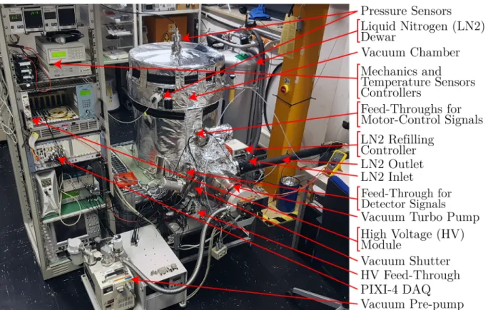
Its special advantage is the possibility to use β- and α-radiation and potentially also a LASER to examine a detector. This is possible because the detector and the sources of radiation are located together in one big vacuum chamber. A picture of GALATEA is shown in Fig. 2.1 while the inside of the vacuum chamber is depicted in Fig. 2.2.
Figure 2.1.: Picture of GALATEA taken October 17, 2016. The most important compo- nents of the test stand are annotated.
2.1. General Setup
2.1.1. Vacuum and Cooling
A vacuum pre-pump and a turbo pump create a vacuum inside the vacuum chamber with a pressure as low as ≈10−7mbar. A cryo tank is located inside the vacuum chamber, right above the bottom plate. It is automatically refilled with liquid nitrogen (LN2) from
an external dewar. The detector under study is thermally connected to the cryo tank through a cooling finger. An issue is infrared radiation from the outer wall, which would increase the leakage current of a germanium detector to a non-acceptable level. Therefore, an electropolished and silver coated copper "hat" surrounds the detector and acts as an infrared shield. Additionally, a cryogenic multilayer foil "COOLCAT 2", close to the outer wall of the chamber, acts as a thermal isolation [15]. When thermal equilibrium is reached during normal operation, the detector has a temperature of ≈90 K.
To start operation, the chamber is pumped down to ≈ 10−7mbar. Then the cryo tank is filled. Its surface acts as an additional cryo pump. This improves the vacuum to levels down to ≈10−9mbar.
The vacuum pumps are shut down for data taking, since they would cause microphonic noise. Therefore, a shutter is closed which separates the pumps from the chamber. Con- sequently, the pressure in the chamber stabilizes around ≈ 10−5mbar during data taking.
This is good enough for detector operation and can be maintained over several weeks.
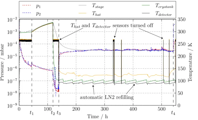
There are two pressure sensors and ten temperature sensors inside and outside of the chamber to monitor the environmental conditions continuously. A typical situation is shown in Fig. 2.3.
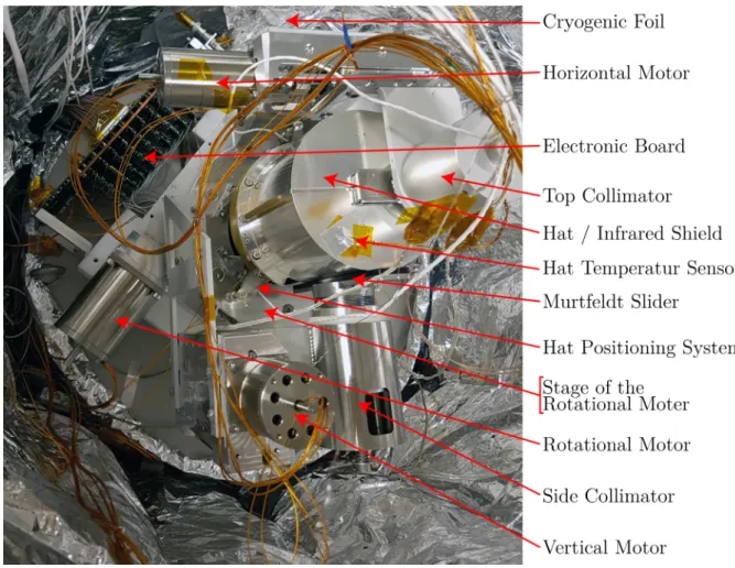
Figure 2.2.: Picture of the inside of the vacuum chamber of GALATEA taken August 3, 2016. The most important components are annotated.
2.1. General Setup
0 100 200 300 400 500
hBK2 f ? 10−9
10−8 10−7 10−6 10−5 10−4 10−3 10−2
S`2bbm`2fK#`
p1
p2
Tstage
That
Tcryotank
Tdetector
0 50 100 150 200 250 300 350
h2KT2`im`2fE
t1 t2 t3 t4
sensors turned off
automatic LN2 refilling Tdetector
Thatand
Figure 2.3.: Pressures and temperatures as observed inside GALATEA, starting August 9, 2016. The two pressuresp1andp2are measured with two pressure sensors. The temperatures,Ti, are measured with four Pt100 sensors. They are placed on the stage of the rotational motor (Tstage), on the top of the cryo tank (Tcryotank), on the top of the hat (That) and on the detector holder (Tdetector). Between t= 0 h and t1, the vacuum turbo pump was switched on, reducing the pressure to≈10−6mbar. Att1, a bake-out process was started, rising the temperature to ≈ 330 K and causing a temporary increase in pressure. At t2, this process was stopped and the automatic LN2 refilling was switched on, decreasing the temperatures and pressure rapidly. Tdetector went down to ≈ 90 K. At t3, the shutter was closed and the turbo pump was switched off. The pressure rose, but became stable at an acceptable level. Data taking started at t3 and ended at t4.
2.1.2. Mechanics
Three remotely controlled motors facilitate almost complete surface scans of the detector under study. They are designed to work at LN2 temperatures and in ultra-high vacuum.
A rotational motor located below the detector holder supports the infrared shield and two linear motors. One motor is mounted vertically and moves a collimator up and down at the side of the hat. The other one is mounted horizontally and moves a collimator radially above the hat. By combining the three motors, nearly every position on the detector surface can be irradiated.
The collimators create beamspots of a few millimeters in diameter. The hat has two slits, along which the two collimators are moved. In order to reduce friction, Murtfeldt layers cover the sliding parts of the collimators.
2.2. Hat Positioning System - HPS
In December 2013, a problem with the rotational movement occurred [14]. According to the original design, the hat was resting on the base plate of the detector holder and had to slide during the rotation of the stage. The problem was, that the friction became too large and the hat dragged the holder along. This damaged the setup, including the detector. As a solution, three screws with stepper motors (Appx. A) were installed below the hat which are used to lift the hat up. In this configuration, the hat can be rotated safely. The hat is lowered for data taking to close the infrared shield. The two configurations that have to be established and verified for secure operation are:
1. The hat must be fully lifted for rotation.
2. The hat must be fully lowered for data taking.
After the initial installation, the screws were able to lift and lower the hat, but it was impossible to verify the required conditions. The problems with the screws are:
• The screws move at different velocities.
• Their movements are not reproducible.
• The number of turns which are set to be executed can not be converted into a distance.
• The screws get stuck when they reach their end positions.
As the screws themselves are not equipped with a positioning system, an external hat positioning system (HPS) had do be designed. Each screw is equipped with an independent HPS as shown in Fig. 2.4.
Each HPS consists of a threaded rod, two steel plates, washers, nuts, two spring contacts and Kapton shielded cables. The two contacts are glued to the steel plates with an isolating glue (Araldite) such that they are electrical isolated from the rest of the HPS. The two steel plates can be fixed at different heights on the rod by precisely adjusting the nuts.
The whole HPS is mounted on the stage of the rotating motor with an extra metal plate.
The two steel plates with the contacts have to be adjusted such, that one is above and the other one is underneath the lower end-piece of the screw, see Fig. 2.4 (left). The two Kapton shielded cables are soldered to the two contacts. These cables have additional mesh shielding and are connected to a D-SUB feed-through. The mesh shielding is connected to the ground pin of the feed-through and to the rod of the HPS, which is in electrical contact with the stage of the rotational motor, which is also grounded.
A voltage can be applied remotely to both contacts through the corresponding pin of the D-SUB feed-through. As soon as the screw touches one of the contacts, a current is measured in the corresponding circuit. The electrical configuration of the HPS is illustrated in Fig. 2.5.
Each HPS has to have its two spring contacts adjusted such that the top (bottom) contact indicates that the hat is sufficiently lifted (lowered) to assure configuration 1. (2.).
2.2. Hat Positioning System - HPS
Figure 2.4.: Photos of a mounted (left) and unmounted (right) HPS. The threaded rod, nuts, washers and steel plates are in electrical contact with the stage of the rotational motor and are grounded over the cable shielding and over the stage to the ground of GALATEA. Two spring contacts are glued to the metal plates with an isolating glue (Araldite) and two Kapton signal cables are soldered to them. On the left, the screw including its stepper motor is also visible.
Figure 2.5.: Illustration of the electrical configuration of the HPS. The gray areas of the HPS, the screw and the rotational stage are in electrical contact. The screw is moved up and down until it makes contact to the upper or lower spring contact closing the corresponding circuit.
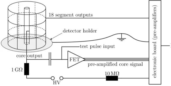
2.3. Read-out Electronics
As stated in section 1.2, Siegfried III is operated at a bias voltage of VB = 4000 V. The segments are grounded by DC coupled amplifiers through the Kapton printed-circuit-board (PCB), visible in Fig. 1.4. The whole electronics configuration is shown in Fig. 2.6.
The core is capacitively coupled to a field effect transistor (FET), directly underneath the detector in its holder. The FETs for the segments are not located directly at the detector, but on the electronic board. There is a significant cross-talk from the core to the segments, because the core read-out cable with the larger signal cannot be kept far away from the segment signal cables. The amplified signals are brought from the electronic board to a data acquisition (DAQ) system outside of the vacuum chamber, for details see [15][14].
Figure 2.6.: Schematic of the read-out electronics of GALATEA. The electronics board contains 19 pre-amplifiers for the core and the 18 segments. The core has the first stage of the pre-amplifier in the detector holder. The segments and core cables are mounted in close proximity in some places. This was unavoidable, because of the rotating parts.
3. Data Taking
The recording of an event is triggered by an energy deposition above a set threshold.
The events originate from different sources. The natural background radiation is always present. Radioactive sources are placed close to the detector to investigate special aspects of the detector response. Two sources were used for the studies presented in this thesis:
228Thorium and 241Americium.
3.1. Background Radiation
The natural background radiation originates from unstable isotopes in the environment and from cosmic radiation. High energetic cosmic radiation produces many particles of lower energy (cosmic showers) when it enters the earth’s atmosphere. Unstable isotopes decay through alpha or beta decays until they become stable isotopes. After each decay, the nuclei are usually in excited states, which deexcite through emission of characteristic photons of discrete energies Eγ.
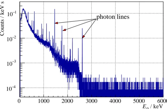
The energy spectrum (number of events with a certain energy per unit time vs. energy) of the background radiation shows characteristic peaks associated to photon lines at char- acteristic values of Eγ. Several background measurements were taken in GALATEA. The spectrum from one of these measurements, BGM, with a duration of 4 h is shown in Fig. 3.1.
A multitude of gamma lines is clearly visible. Five of the most prominent lines are listed in Table 3.1. Each gamma line also produces a continuous contribution to the spectrum due to Compton scattering. In GALATEA, the background causes an event rate of ≈ 90 Hz with a core threshold of ≈20 keV.
Isotope Eγ / keV
214Pb 351.932±0.002
214Bi 609.312±0.007
40K 1460.830±0.011
214Bi 1764.494±0.014
208Tl 2614.533±0.013
Table 3.1.: Dominant gamma lines in the natural background radiation as measured in GALATEA. The values of Eγ are taken from [18][19].
3.2. Uncollimated Thorium-228 Source
Thorium-228 is an unstable isotope, which decays via the228Th decay chain with alpha and beta decays until it becomes 208Pb [19]. The most dominant gamma lines from this chain are listed in Table 3.2 [18]. For this study, a two-hours long 228Th measurement (THM)
/ keV E0
0 1000 2000 3000 4000 5000 6000
Counts / keV s
−4
10
−3
10
−2
10
−1
10
photon lines
Figure 3.1.: Energy spectrum of the core channel from a an four-hours long background measurement measured in GALATEA. The photon lines have discrete energies.
was performed, where the thorium source was placed on top of the vacuum chamber, illuminating the whole detector.
Isotope Eγ / keV
212Pb 238.632±0.002
208Tl 510.77±0.10
212Bi 727.330±0.009
208Tl 860.564±0.005
208Tl 2614.533±0.013
Table 3.2.: Unstable isotopes of the Th decay chain and their corresponding gamma ener- gies. Only the most dominant ones are listed.
3.3. Collimated Americium-241 Source
3.3. Collimated Americium-241 Source
Americium-241 is an unstable isotope, which decays via the241Am decay chain with alpha and beta decays until it becomes209Bi [19]. The first decay has several alpha decay channels to237Np with discrete energies,Eα. The most dominant decay hasEα = 5485.56±0.12 keV, with a branching ratio of 84.5 %. The resulting237Np nucleus is in an excited state and de- cays through the emission of one gamma with an energy ofEγ = 59.5412±0.0002 keV [18].
Alpha particles are double-positively charged bare helium nuclei and experience a strong electromagnetic interaction with matter. In air, alphas of a few MeV only penetrate a few centimeters and in solid matter, like germanium, they penetrate just a few micrometers.
Therefore, alphas are suitable to investigate surface effects of germanium detectors. For photons in the lower keV region, like the 59.5 keV gammas from241Am, the most dominant interaction is photoelectric absorption. Most of these gammas are absorbed within≈5 mm of germanium, so they also interact relatively close to the surface.
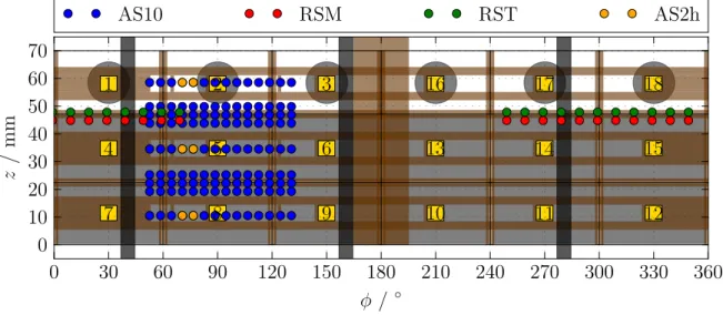
A241Am source was placed inside the side collimator of GALATEA. For this study, several side scans, listed in Table 3.3 and mapped in Fig. 3.2, were performed.
Label tm Description
RST 1 h Rotational scan over 180◦ in the top row of segments.
RSM 1 h Rotational scan over 180◦ in the middle row of segments.
AS10 10 min 126 measurements in a 14×9 geometry covering segments 1 to 9.
AS2h 2 h 6 measurements in segments 2,5 and 8.
Table 3.3.: Side scans of Siegfried III with a collimated 241Am source. tm is the duration of each measurement within the scan.
..
0
.
30
.
60
.
90
.
120
.
150
.
180
.
210
.
240
.
270
.
300
.
330
.
360
.
ϕ / ◦
.
0
.
10
.
20
.
30
.
40
.
50
.
60
.
70
.
z/mm
.
1
.
2
.
3
.
16
.
17
.
18
.
4
.
5
.
6
.
13
.
14
.
15
.
7
.
8
.
9
.
10
.
11
.
12
.
AS10
.
RSM
.
RST
.
AS2h
Figure 3.2.: Map of measurements performed with a collimated 241Am source. The dot sizes do not reflect the size of the beam spot for reasons of clarity. At the positions of the AS2h measurements (orange), also measurements belonging to AS10 (blue) were performed.
3.3.1. Size of the Beam Spot
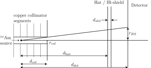
The collimator consists of five coaxial copper segments. Copper was chosen as the col- limating material, because it does not introduce X-Rays close to the 59.5 keV line. The collimator creates a narrow beam, shining onto the detector mantle. A detailed study on different collimator configurations and resulting beam spots can be found in [15]. The principle of the calculation to determine the radius of the beam spot, rBS, is illustrated in Fig. 3.3.
Figure 3.3.: Illustration (not to scale) of the collimator and detector geometry. The source is located inside the collimator, which is mounted to the vertical motor inside GALATEA. The collimator creates a narrow beam directed onto the mantle of the detector.
Assuming a point source, rBS for low energy photons is rBS ≈ rcol
dcolddet = 2.7 mm , (3.1)
whereas dcol = 40 mm is the distance from the source to the end of the last collimator segment, ddet = 67 mm is the distance from the source to the detector mantle and rcol = 1.6 mm is the inner radius of the collimator segments.
For the alphas, also the copper hat with a thickness of 4 mm acts as a collimator, but only in horizontal direction. The slit of the hat has a width of dslit= 2 mm and the distance of the source to the hat is dhat = 47 mm. Therefore, by adapting Eq. 3.1, an elliptical beam spot with a vertical radius of 2.7 mm and a horizontal radius of 1.5 mm, is produced.
4. Data Acquisition and Processing
4.1. Data Acquisition System (DAQ)
As explained in section 2.3, the charged induced signalsQindi of each channel i (i∈[0,18], 1 core plus 18 segments) are amplified inside the vacuum chamber and than brought to a (PIXIE-4 [20]) DAQ outside the chamber. The DAQ has an analogue to digital converter (ADC) which digitizes the analog signals into 14-bit long unsigned integers, counts, with a sampling rate of 75 MHz. It stores the last 1023 samples (≈ 13.64 µs) of all channels temporarily in a small memory, called the buffer. The samples have a temporal distance of
≈ 13.33 ns. If an event occurs, the entire buffer is stored to a hard disk. Thus, one event consists of 19×1023 data points prawi (k), k ∈ [1,1023], or prawi (t) with t = k ·13.33 ns respectively. These prawi (k) represent the pulses.
The algorithm, with which the DAQ recognizes an event (trigger), is the so-called sliding trapezoidal filter [20]. The DAQ is set to trigger on the core pulse, since the core is the single n-contact of the detector, and therefore, an event always creates a recognizable pulse in the core channel. A feature of the sliding trapezoidal filter is that the signal pulse occurs always roughly at the same samplek, i.e. the same time.
The ADC is set to have an offset, because noise can causeprawi (k) to be negative and this information would be lost by the conversion into positive integers. The polarity of the core channel is always flipped, because it would always show a negative signal, since the core collects electrons. The signals from the amplifiers always show an exponential decay due to discharging processes. The offset and the decay are corrected for during the pulse preprocessing.
4.2. Pulse Preprocessing
Figure 4.1 shows the different stages of the pulse preprocessing-procedure for a regular pulse in the core channel. A regular pulse has a flat baseline until the signal starts, rising rapidly as soon as the electron hole pairs start drifting. After the charge carriers are fully collected, the decay of the pulse becomes visible.
..
0
.
2
.
4
.
6
.
8
.
10
.
12
.
t /µs
.
0
.
5000
.
10000
.
15000
.
20000
.
ADC
.
praw
.
pbls
.
ptdc
Figure 4.1.: The different stages of the pulse preprocessing of a regular pulse in the core channel are shown. The green line represents the raw data and the red line the interim result after baseline subtraction (bls). The black line is the final result after decay correction (tdc).
4.2.1. Baseline Correction
The offset is calculated by determining the level of the baseline for each pulse. It is defined as the average of the first 337 samples:
¯
pBLi = 1 337
337
X
k=1
prawi (k) . (4.1)
This offset is removed by subtracting it from each sample
pblsi (k) = prawi (k)−p¯BLi , (4.2) where bls stands for "baseline subtracted". The result is shown in Fig. 4.1 (red line).
4.2.2. Decay Correction
The decay constants of the pre-amplifiers are ≈ 50 µs, but differ slightly from channel to channel. The exact values for each channel are calculated by fitting an exponential to the decay part (≈ last 7 µs) of a large sample of regular pulses. The resulting decay constants form Gaussian distributions with mean values, which are taken as the decay constants, τi, of pre-amplifier, i. The values forτi are listed in App. B.1. They were calculated from the BGM data set, see section 3.1, and were applied to all pulses for this study.
4.3. Measured Pulse Amplitudes
The decay correction is applied iteratively:
ptdci (1) =pblsi (1) (4.3)
ptdci (2) =pblsi (2) +ptdci (1)−pblsi (1)·exp−13.33 ns τi
(4.4)
...
ptdci (k) = pblsi (k) +ptdci (k−1)−pblsi (k−1)·exp−13.33 ns τi
, (4.5)
whereastdc stands for "tau decay corrected". The result is shown in Fig. 4.1 (black line).
The decay correction is already applied during the rise of the pulse. This is correct because the discharge already starts as soon as charge is collected.
4.3. Measured Pulse Amplitudes
After the pulse preprocessing, the measured pulse amplitude in dimensionlessADCcounts, Mi, are determined. They correspond to the induced chargesQindi and therefore also to the energy Ei deposited in segment i. Two time windows are defined to determine Mi. The first one is the baseline window, ranging from sample 1 to sample 337. The second one covers samples 525 to 1023. Both windows are illustrated in Fig. 4.2.
..
0
.
2
.
4
.
6
.
8
.
10
.
12
.
t / µs
.
0
.
2000
.
4000
.
6000
.
8000
.
10000
.
12000
.
ADC
.
baseline window
.
signal window
.
ptdc
Figure 4.2.: Illustration of the two time windows defined for the determination of the pulse amplitude,Mi. The baseline window extends fromk= 1 tok = 337, the signal window fromk = 525 to k = 1023.
Mi is defined as the difference of the pulse averages from the two windows:
Mi = 1 498
1023
X
k=525
ptdci (k)− 1 337
337
X
k=1
ptdci (k) , (4.6)
where the second term on the right should be 0, since the window is the same as used for the baseline subtraction. For an ideal event (complete and fast charge collection in one
segment i and core) without any cross-talk, the relation
Edeposited ∝Qind0,i ∝M0,i (4.7)
would hold and for all other channels (j 6= 0, i),Mj = 0. But due to cross-talk, this relation does not hold and the reconstruction of events becomes more complex.
4.4. Cross-talk and Amplifications
For Siegfried III in GALATEA, there are two sources of cross-talk. The first one is intrinsic cross-talk due to the capacitive coupling between the detector electrodes. This cross-talk can be described with a matrix Ci
Ci =
1 ci0,1 . . . ci0,18 ci1,0 1 ... ...
... ... ... ci17,18 ci18,0 . . . ci18,17 1
. (4.8)
The second one is the cross-talk due to the capacitive coupling between the signal cables.
It is described with the matrix Ce
Ce=
1 ce0,1 . . . ce0,18 ce1,0 1 ... ...
... ... ... ce17,18 ce18,0 . . . ce18,17 1
. (4.9)
For the proper treatment of these two sources of cross-talk, the different stages of signal amplification have to be taken into account. As mentioned in section 2.3, the core FET is mounted close to the detector, whereas the segment FETs are integrated on the electronics board. This can be described with the matrices F
F=
f0 0 . . . 0 0 1 ... ...
... ... ... 0 0 . . . 0 1
(4.10)
for the core amplification close to the detector andAfor the amplification on the electronics board:
A=
a0 0 . . . 0 0 a1 ... ...
... ... ... 0 0 . . . 0 a18
. (4.11)
Under the assumption of linearity (neglecting second order cross-talk), the following relation between the vector of channel energies #»
E = (E0 ... E18) and the vector of measured pulse
4.5. Reconstruction of the Energies amplitudes # »
M = (M0 ... M18) holds:
E#»·Ci ·F·Ce·A = # »
M , (4.12)
E#»·C0 = # »
M , (4.13)
where the four matrices Ci, F,Ce and A can be combined to one 19×19 matrix C0 with matrix elements c0i,j.
4.5. Reconstruction of the Energies
By inverting C0, a set of 19 equations is obtained to reconstruct the channel energiesEi: E#»= # »
M ·C0−1 . (4.14)
The problem is to determine the coefficients c0i,j. In order to do so, two assumptions were made:
• The core energy is equal to the sum of the segment energies:
E0 =X18
j=1
Ej . (4.15)
• The cross-talk from each segment to the core is the same:
cj,0 =const.=c1,0 ∀ j ∈[1,18] . (4.16) The first assumption reflects conservation of energy. The second one is needed to allow for determiningE0 fromM0 only. The argument for this condition is that the cross-talk from the core to the segments is much stronger than the cross-talk from the segments to the core. Therefore, the small deviations between the cj,0 are neglected.
4.5.1. Core Energy
The core energy E0 is determined as proportional to M0. According to Eqs. 4.13, 4.15 and 4.16,
M0 =X18
i=0
Ei·c0i,0 =E0·c00,0+X18
i=1
Ei·c0i,0 (4.17)
=E0·c00,0+c01,0·
18
X
i=1
Ei =E0·(c00,0+c01,0) =E0·ccore , (4.18) whereccore is defined as c00,0+c01,0.
Known photon lines, listed in Table 4.1, in the core ADC-spectrum of all events are fitted to determine ccore. The mean ADC-values and the known photon energies are input to a linear fit providing ccore. E0 is calculated as
E0 =M0/ccore (4.19)