lows building very thin detectors with high spatial resolution and low power consumption. However, high readout speeds of 50 MHz line rate and 20 kHz for the full detector must be reached. A pro- totype system is presented, using a new DEPFET pixel matrix (128 64 pixels), fast steering chips (Switcher II) for row wise oper- ation and a fast current based readout chip (CURO II). The sen- sors with small linear DEPFET pixels(22 36 m2)are opti- mized for fast readout and high spatial resolution. Measurements show that the complete removal of the accumulated signal charge from the internal gate (complete clear), which is fundamental for the foreseen readout mode, is feasible. The current based readout chip CURO II, containing current memory cells, pedestal subtrac- tion and on chip zero suppression for a triggerless operation has been fabricated and tested. First results of a full prototype system are presented.
Index Terms—Active pixel sensor, CURO, DEPFET, Interna- tional Linear Collider (ILC), vertex detector.
I. INTRODUCTION
THE HIGH energy electron-positron collider ILC (Inter- national Linear Collider) is the ideal complement to the hadron collider LHC, allowing excellent efficiency and purity in the flavor identification of hadronic jets. The separation be- tweenb andcdecay tracks and the distinction between their primary, secondary, and tertiary vertex should become possible.
In order to minimize multiple scattering contribution to the im- pact parameter resolution the reduction of material of sensor and cooling in the detector area requires close attention. Conse- quently a thin detector with high signal to noise and low power consumption is needed.
In addition the background conditions and time structure of the accelerator influence the the design of the vertex detector.
Due to very prominent beamstrahlung near the interaction point the number of hits in layer 1, typically situated at a radius of 15 mm just outside the beam pipe, for each bunch crossing and per mm is 0.03 (0.05) for and a magnetic field of 4 T [1]. With a bunch structure of 2820 bunches within 950 s it becomes inevitable to keep the pixel size small and
Manuscript received November 15, 2004; revised March 22, 2005. This work was supported by the Ministerium für Wissenschaft und Forschung (BMBF) of Germany under Contract 05 HS2PD1/1.
R. Kohrs, M. Karagounis, H. Krüger, L. Reuen, C. Sandow, M. Trimpl and N.
Wermes are with the Physikalisches Institut, Universität Bonn, D-53115 Bonn, Germany (e-mail: kohrs@physik.uni-bonn.de).
L. Andricek, G. Lutz, H. G. Moser, M. Porro, R. H. Richter and L. Strüder are with the MPI Halbleiterlabor, D-81739 München, Germany.
P. Fischer, M. Harter and I. Peric are with the Insitut für Technische Infor- matik, Universität Mannheim D-68131 Mannheim, Germany.
Digital Object Identifier 10.1109/TNS.2005.852719
Fig. 1. Schematic cross section of the DEPFET pixel detector.
read out the detector several times during the train in order to keep the detector occupancy at a level that does not compromise the track reconstruction.
II. Depleted Field Effect Transistor (DEPFET) CONCEPT FOR
A -LINEARCOLLIDER
In the DEPFET Pixel concept as shown in Fig. 1 the first am- plifying p-channel transistor is integrated into a fully depleted high resistivity silicon substrate [2].
By sideward depletion and an additional -implantation below the FET, a potential minimum for electrons is created right underneath the transistor channel which can be considered as an internal gate of the FET. The signal electrons created by an impinging particle are collected and stored in the internal gate, which leads to a change in the potential of the internal gate resulting in a modulation of the transistor channel current. As the operating state of the FET has no impact on the collection of signal charge, the dead time and the power consumption can be held extremely low. Due to the nondestructive readout of the pixel device the charge in the internal gate has to be removed from time to time. This “clearing” is obtained by periodically applying a positive voltage pulse to a separate contact at the border of each pixel (pulsed clear mechanism). Other clear mechanisms have also been studied [3].
In this concept, stray capacitances due to connections be- tween sensor and amplifier are vastly reduced and a very small input capacitance can be realized. This leads to an excellent noise performance which allows high energy resolution and
0018-9499/$20.00 © 2005 IEEE
1172 IEEE TRANSACTIONS ON NUCLEAR SCIENCE, VOL. 52, NO. 4, AUGUST 2005
Fig. 2. Principle of operation of a DEPFET pixel matrix.
thin sensors. With single isolated DEPFET pixels, an equivalent
noise charge of at room temperature has
been measured [4]. For a large DEPFET matrix operated at the high readout speed required for the ILC, a total noise figure of or less is aimed for. In addition to the excellent signal to noise ratio new sensor devices enable small pixel sizes in large matrices and low power consumption. These features make DEPFET pixels very attractive for future particle physics experiments, especially those at a planned linear collider.
The readout concept for arrays of DEPFET pixels is illus- trated in Fig. 2. The gate and clear contacts of the pixels are interconnected row-wise by aluminum traces, wire bonds are used for the connection with the steering chips. The drains of the transistors are interconnected column-wise and can be con- tacted at the bottom and/or top of the matrix to the readout chip.
The pixels are read out row-wise by applying a voltage to the external gates of the DEPFETs. As mentioned above, switching off the pixels is possible independently of the amount of charge carriers in the internal gate, in particular the sensitivity is not affected by the operating condition of the FET. At the bottom of each column the current of the active pixel is transferred to one channel of the readout chip. This allows random access to the individual pixels in the matrix.
The expected occupancy at the innermost layer of the ILC vertex detector requires a readout rate of 20 kHz [1]. For an envisaged matrix size of 400 5000 pixels this leads to line rates of 50 MHz with the matrix being read out from both sides.
The total power consumption has been calculated using mea- sured currents and voltages of the chips and matrices described below and assuming that they can be switched off between sub- sequent bunch trains, as a duty cycle of 1/200 is foreseen at the ILC. Scaled to the total pixel vertex detector [1] primarily de- signed for TESLA with five layers, the sensor is expected to have a power consumption of 0.3 W, while the integrated cir- cuits (ICs) consume 3–4 W (steering) and 1–2 W (readout),
respectively. Hence, we consider a total power budget of less than 5 W for the entire vertex detector is feasible.
III. THEPROTOTYPESYSTEM
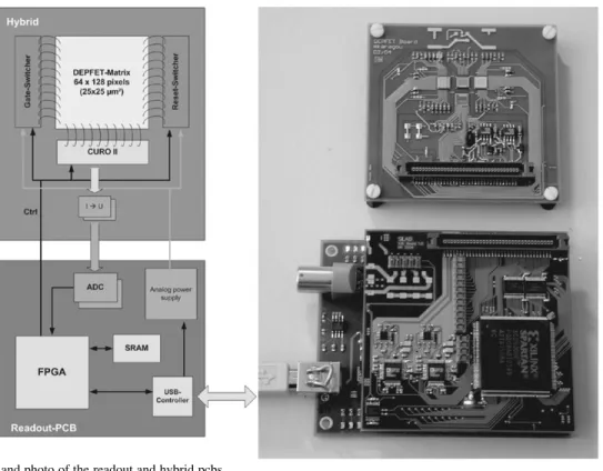
In the development to this goal a USB-based prototype system, including a new DEPFET matrix with small pixels and dedicated ASIC chips for fast steering and current based readout, has been developed. The main components of the system are shown in Fig. 3.
For greater flexibility with regard to laser or testbeam setups it is subdivided into two parts, connected by a ribbon cable.
The sensor matrix as well as the ASICs for steering (Switcher II) and readout (CURO II) are assembled on one hybrid PCB, while the digitally parts like FPGA, USB controller, ADCs and RAM are assembled on a separate PCB. Besides those PCBs only external power supplies and a PC are needed for operation.
In the following the main components of the system will be discussed.
A. Switcher II
The selection of a particular row as well as the Clear are con- trolled by the 2 64 channel SWITCHER II chips, which are developed in Bonn in 2002 and fabricated with an AMS 0.8 m high-voltage process. The chip is capable of switching voltages up to 20 V with frequencies of 30 MHz. A RAM on the chip stores the control sequence allowing operation modes with no external control signals. Several chips can be daisy chained if more than 64 channels are to be addressed. For a detailed de- scription of the Switcher chip see [5].
B. Curo II
The 128 channel CUrrent Readout Chip (CURO II) was de- veloped in Bonn and fabricated at TSMC in a 0.25 m CMOS
Fig. 3. Block diagram and photo of the readout and hybrid pcbs.
technology with a radiation tolerant design. The readout archi- tecture is based on a current mode signal processing scheme, well adapted to the output of the DEPFET pixels, which are currents, not voltages. The principle of the readout is shown in Fig. 4.
The functionality of the readout chip can be separated into two major parts.
In the first part, a regulated cascode keeps the pixel drain at a constant potential, eliminating the influence of the large sensor capacitance and the effect of the limited output conductance of the pixel transistor itself. After selecting one row of the matrix, the current is stored in a fast current memory cell. By applying a positive voltage pulse to the Clear contacts of the same row the accumulated signal charge is removed from the internal gate.
The so derived pedestal current is subtracted from the buffered current automatically at the output node of the memory cell due to its inverting character. The resulting signal current is stored in a further memory cell.
In the second part of the readout chip, a digital hit pattern is determined by comparing the buffered currents of a row with individual thresholds in parallel. Since only those memory cells with values above the threshold are needed, all other cells are switched off in order to save power. A digital hit finder identi- fies up to two hits in the digital pattern of a row per cycle and processes a row until no more hits are found. The pixel address, i.e., row and column, of an identified hit is stored in a digital hit buffer, while the corresponding analog value is multiplexed to one of the two output channels immediately. A more detailed description is given in [6].
C. Readout Board
The output current of CURO is converted into a differential voltage signal by an external low noise and fast transimpedance amplifier, then digitized by a 14-bit analog-to-digital (ADC) and
Fig. 4. Readout principle of CURO II.
stored in SRAM cells for a subsequent readout. The slow con- trol and readout of the chips, the sophisticated timing, the fast
1174 IEEE TRANSACTIONS ON NUCLEAR SCIENCE, VOL. 52, NO. 4, AUGUST 2005
Fig. 5. Circuit of a Test Matrix pixel cell.
storage of ADC values in the RAM and the data transfer to the PC via USB is managed by a SPARTAN 3 FPGA. Furthermore, a software-programmable Sequencer inside the FPGA is used to control and optimize readout modes easily. The main system clock is digitally adjustable in a wide range. In order to mini- mize crosstalk all clock signals are distributed as LVDS signals.
D. CMOS Test Matrix
In order to show the functionality of the readout system in- dependently from the properties of a new DEPFET matrix, a dedicated CMOS Test Matrix has been developed [7] and fab- ricated in CMOS 0.35 m technology. Since the CMOS 3.3-V technology is well understood, such a test matrix is much easier to integrate in a new system than a DEPFET matrix and is thus very valuable for debugging purposes. The Test Matrix has 64 128 cells with an identical pad layout as the DEPFET coun- terpart. Every pixel cell contains an NWELL-PSUB photodiode and a circuitry that generates an offset current and an illumina- tion dependent current, analog to an increase of DEPFET cur- rent caused by an impinging particle.
The circuit of a pixel cell is shown in Fig. 5. The offset cur- rent of A is generated by a constant current source M2, whereas the voltage controlled signal current source is regulated by the voltage across capacitor M5. Capacitor M5 is charged by the photo current generated in the photo diode. By closing the Select switch M3 the sum of signal and offset current is applied to the output of the pixel cell. The reset mechanism is designed in a way, that the capacitor M5 is not discharged to zero, but to the threshold voltage of transistor M1. Thus, the illumination of a pixel cell after a reset leads to an increase of the output current instantaneously. The normal way of discharging M5 to the threshold voltage of M1 would be using a very small refer- ence current of the current mirror given by M9. But that slows down the reset procedure. Therefore, a larger reference current of A is used but the W/L of transistor M6 is chosen 30 times larger than the W/L of transistor M1. Thus, the signal cur- rent after a reset is in the regime of nano amperes and is therefore negligible compared to the offset current. The time required for the reset has been measured to 6 ns [7].
Fig. 6 shows a picture taken with the prototype system, using a simple webcam lens mounted on the hybrid equipped with a CMOS Test Matrix. The readout of the 128 64 pixels was done within 1 ms, which is equivalent to 120 ns per pixel.
Fig. 6. Picture taken with full prototype system equipped with CMOS Test Matrix and webcam lens. (from left to right: R. Kohrs, C. Sandow, M. Trimpl, and H. Krüger.
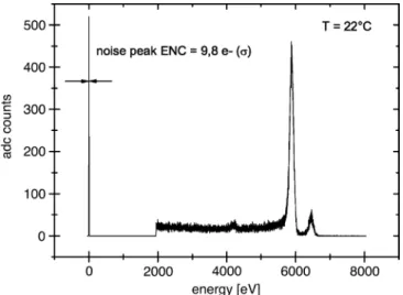
Fig. 7. F e spectrum taken with a linear DEPFET structure at room temperature.
E. DEPFET Matrix
The DEPFET matrices are processed in a MOS technology with two polysilicon and two metal layers on high ohmic n- substrate, developed and fabricated in 2004 at the semicon- ductor laboratory of the Max-Planck-Institutes in Munich [8].
Along with the R&D for HEP vertexing, the DEPFET tech- nology was changed from JFETs to MOSFETs as MOSFETs have a number of advantages, e.g., allowing much smaller pixel sizes, providing a better homogeneity and a potentially higher internal amplification. A very compact linear pixel cell geometry has been introduced, where the implanted drain, source and clear regions are shared by neighboring cells (double pixels). Furthermore, a polysilicon structure, the so called “clear gate,” supports the clear process, and acts as an isolation frame between clear region and internal gate during the charge collection. A variety of slightly different structures were processed in order to determine the optimal parameters by means of the fabrication process, pixel size, charge collection efficiency and clear efficiency. The smallest pixel size so far is m . Simulations have confirmed that no potential pockets, which can trap signal charges during charge collection and clearing, exist in the design. A more detailed description is given in [8].
The figure of merit of the DEPFET is the transconductance of the internal gate , where is the change of
Fig. 8. Readout sequence of a DEPFET with “on the fly” pedestal subtraction.
Fig. 9. Difference between two current samples. The hatched area indicates an efficient clear.
the drain current and dQ is the collected charge in the internal gate. A value of has been measured in very good agreement with the simulations.
Equivalent Noise Charges of have been
measured with a linear double pixel structure at room tempera- ture (Fig. 7).
One contribution to the overall noise of the signal is the in- complete removal of charges of the internal gate, as the pedestal subtraction in CURO is done “on the fly” (see Fig. 8).
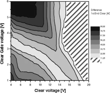
The difference of the two current samples taken by CURO is thus not just the pure signal value but also the uncertainty of charge left in the internal gate after an incomplete clear. There- fore, a complete clear is essential. Measurements on double pixels and small matrices show that a complete clear is feasible with moderate voltages of 14 V, which is easily achievable with the Switcher chip.
Shown in Fig. 9 is the difference of two current samples, with a charge injection by laser and a subsequent clear pulse in be- tween. In the case of a residual current of zero the charge in the internal gate is the same before and after the clear, but not nec- essarily zero. The proof of acompleteclear is shown in Fig. 10, where the width of the noise peak obtained by measuring the DC DEPFET drain current is plotted, using two different readout op- erations: 1) a single Clear pulse followed by 500 samples and 2)
Fig. 10. Evidence for a complete clearing of the internal gate for voltages larger than 14 V.
500 individual Clear pulses, immediately followed by a readout sample. If the charge removal is complete the clear noise con- tribution vanishes and the noise level drops, thus, the widths of the noise peaks in both cases should be the same.
IV. CONCLUSION
A full prototype system including a new DEPFET matrix and dedicated ASIC chips for steering and readout have been devel- oped addressing the demanding requirements of the ILC.
Performance measurements on the main components of the system can be summarized as follows:
• the steering chip Switcher 2 is versatile and works fine up to 30 MHz providing voltage levels sufficiently for a complete clear;
• all measurements done on the readout chip CURO with its fast current memory cells, correlated double sampling, on-chip pedestal subtraction and triggerless zero suppres- sion are in agreement with the simulated performance;
• the new DEPFET matrices with small pixel sizes show low noise, complete clear, and an improved internal gain.
The functional efficiency of the prototype system was ad- duced with a dedicated CMOS Test matrix. It is now ready for operation with the new DEPFET matrices, which have already been tested separately. The full system will be characterized in a testbeam in the beginning of 2005.
REFERENCES
[1] “TESLA—Technical Design Report,” DESY, Germany, ISBN 3-935702-00-0, 2001.
[2] J. Kemmer and G. Lutz, “New semiconductor detector concepts,”Nucl.
Instrum. Meth. A, vol. 253, p. 365, 1987.
[3] P. Kleinet al., “Study of a DEPJFET pixel matrix with continous clear mechanism,”Nucl. Instrum. Meth. A, vol. 392, p. 254, 1997.
[4] N. Wermeset al., “New results on DEPFET pixel detectors for radiation imaging and high energy particle detection,”IEEE Trans. Nucl. Sci., vol.
51, no. 3, pt. 3, pp. S. 1121–1128, Jun. 2003.
[5] I. Peric, “Design and realization of integrated circuits for the readout of pixel sensors in high-energy physics and biomedical imaging,” Ph.D.
dissertation, Physical Institute, Bonn, Germany, 2004.
[6] M. Trimplet al., “A fast readout using switched current techniques for a DEPFET-pixel vertex detector at TESLA,”Nucl. Instrum. Meth. A, vol.
511, p. 257, 2003.
[7] M. A. Karagounis, “Entwicklung analoger integrierter Schaltungen für pixeldetektoren,” Diploma thesis, Physical Institute, Bonn, Germany, 2004.
[8] R. H. Richteret al., “Design and technology of DEPFET pixel sensors for linear collider applications,”Nucl. Instrum. Meth. A, vol. 511, p. 250, 2003.