First results of DEPFET based Active Pixel Sensor prototypes for the XEUS Wide Field Imager
J. Treis
a, P. Fischer
b, O. H¨ alker
a, M. Harter
b, S. Herrmann
a, R. Kohrs
c, H. Kr¨ uger
c, P.
Lechner
d, G. Lutz
e, I. Peric
c, M. Porro
f, R. H. Richter
e, L. Str¨ uder
a, M. Trimpl
c, N. Wermes
ca
Max-Planck-Institut f¨ ur extraterrestrische Physik, Giessenbachstraße, 85748 Garching, Germany;
b
Lehrstuhl f¨ ur Schaltungstechnik und Simulation, Universit¨ at Mannheim, D7 2-4, 68159 Mannheim, Germany;
c
Physikalisches Institut der Universit¨ at Bonn, Nußallee 12, 53112 Bonn, Germany;
d
PNSensor GmbH, R¨ omerstraße 28 , 80803 M¨ unchen, Germany;
e
Max-Planck-Institut f¨ ur Physik, F¨ ohringer Ring 6, 80805 M¨ unchen, Germany;
f
Dipartimento di Elettronica e Informazione, Politecnico di Milano, Via Golgi 40, 20133 Milano, Italy
ABSTRACT
The concept of an Active Pixel Sensor (APS) based on the integrated detector/amplifier structure DEPFET (DEpleted P-channel Field Effect Transistor) has been developed to cope with the challenging requirements of the XEUS Wide Field Imager. The DEPFET-APS combines high energy resolution, fast readout, and random accessible pixels allowing the application of flexible readout modes. First prototypes of DEPFET-based Active Pixel Sensors with a 64 x 64 pixel format and 75 µm x 75 µm pixel area have been produced at the MPI semiconductor laboratory. The APS is read out row by row, i.e. the pixel signals of one row are processed in parallel by a 64 channel CMOS amplifier/multiplexer chip of the CAMEX type. The addressing of one row of pixels for readout and reset is done by two control chips of the SWITCHER type fabricated in a high-voltage CMOS technology. The processing time for one row is of the order of a few micro-seconds. APS operation, the control and data acquisition system are described, and first experimental results are presented.
Keywords: XEUS, X-Ray, DEPFET, Active Pixel Sensor, Imaging, Data acquisition, Spectroscopy
1. INTRODUCTION
The DEPFET concept was introduced in 1987,1 first prototype devices were manufactured soon after.2 By now, several prototypes have been manufactured and were subject to intense studies,3, 4 and DEPFET APS based sensors turned out to be a promising new concept for both imaging applications and high resolution spectroscopy. With the advancement of technology,5 DEPFET based large-area sensors come within reach, and a design concept for the Wide Field Imager (WFI)6, 7 of the X-ray Evolving Universe Spectroscopy (XEUS)8, 9 mission has been proposed, which includes an APS array with an area of 76.8 ×76.8 mm2, divided into 1024
×1024 pixels.10 A prototype production of DEPFET sensors dedicated to XEUS has recently been finished at the MPI semiconductor laboratory in Munich.
In contrast to earlier devices, which used JFETs as amplifying transistors, the sensors of the new production use MOSFETs instead, for the sake of homogeneity and reproducibility for future large area sensors. Besides various single pixel test structures, a number of prototypes of DEPMOSFET matrices have been produced.
First experimental results with single DEPMOSFET structures have been presented earlier10; the progress made on operating and understanding DEPMOSFET structures is presented elsewhere.11 Here, the concept of the DEPMOSFET matrices, their integration into a readout system and very first results of prototype tests are described.
Further author information: (Send correspondence to J. Treis)
J. Treis: E-mail: jft@hll.mpg.de, Telephone: +49 89 83940045, Fax: +49 89 83940013
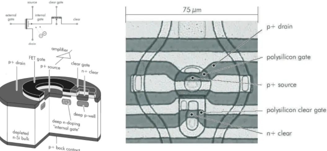
Figure 1.Cutaway (left) and microscope photography of a DEPMOSFET pixel. (right). The pixel consists of a p-channel MOSFET with attached clear region, which can be considered as an additional ’parasitic’ n-channel MOSFET contacting the internal gate. The circular polysilicon gate has a width of 5µm and a circumference of 40µm. The bright horizontal lines are the metal connections of drain, gate, clear and cleargate. The source is connected in vertical direction by the curved polysilicon gates.
2. DEPMOSFET DEVICES 2.1. Principle of operation
A DEPFET (DEpleted P-channel Field Effect Transistor) basically consists of a p-channel field effect transistor, which may either be a MOSFET or a JFET, integrated on the surface of a high resistivity n-type silicon bulk.
Making use of the principle of sideways depletion,12 the silicon bulk can be fully depleted using the reverse biased p+-doped backside diode and the p+-doped source and drain contacts of the FET. By applying an appropriate backside voltage, a parabolic potential distribution with a minimum close to the upper surface of the bulk for electrons is generated. The minimum can be further confined in lateral direction to the area below the transistor channel by an additional n-doped region, which also increases the depth of the potential minimum.
Whenever electron-hole pairs are generated in the silicon bulk they will be separated by the electric field. The holes drift to the backside contact and the electrons are collected in the potential minimum below the transistor channel. Here, they modify the charge carrier density by inducing an additional amount of holes. Thus, the FET channel conductivity is a function of the amount of charge stored in its potential minimum, which is therefore called internal gate. Depending on the biasing condition of the transistor, a change of the channel conductivity may either cause a change of transistor current or a voltage step at, for instance, the source terminal of the FET.
As charge is accumulated in the internal gate, the potential minimum continuously fills up until a dynamic equilibrium is reached, in which the internal gate loses its charge storage capability. Thus, the accumulated charge has to be removed from the internal gate regularly by applying positive voltages to the so-calledclear- contact, an n+-doped region close to the internal gate.
Recently, a first production of DEPFET prototype structures has been finished at the MPI semiconductor laboratory in Munich, which use a MOSFET as transistor. The structures are designed as prototypes for the XEUS WFI and have circular transistor geometry. The clear region for these structures consists of the clear contact and an additional surrounding MOS structure, the so-calledcleargate. The cleargate is kept at negative voltages during integration to prevent charge loss to the clear contact. During the clear process, positive voltages are applied to remove the potential barrier between internal gate and clear, thus ensuring the complete transfer of the internal gate charge to the clear. The clear contact is additionally separated from the detector bulk by a deep p-implanted well. Clear and cleargate together can be considered as a parasitic n-channel MOSFET with the internal gate as source and the clear contact as drain. Figure 1 shows a cutaway of a circular DEPMOSFET structure with attached clear region and a microscope photography of a pixel.
The DEPMOSFET structures for XEUS are dedicated for source follower readout, a readout mode suitable for
Figure 2.Simplified interconnection scheme of pixels on the DEPMOSFET matrix protoypes for XEUS. All pixel drains are connected to a common drain contact. The gates, cleargates and clear contacts of the pixel of a row are connected together, while the pixel sources are connected column-wise. Each column is biased by an external current source. If only one pixel row is active, the signal of a pixel in that row can be taken from the corresponding column source node.
high resolution spectroscopic measurements. Drain and gate voltages of the pixel are fixed, and the pixel source is contacted by a constant current source. A change in the MOSFET channel conductivity yields a voltage step at the source node proportional to the amount of charge collected.
The internal gate of a pixel is capable of storing signal charges regardless of the presence of a transistor current, so the transistor current can be turned off if the signal information is not read out to reduce power consumption.
Additionally, signal detection can be done by comparing the current levels before and after a certain signal integration interval. As the complete clear provides for a reproducible baseline, comparing the current levels in the pixel before and after the clear process provides the signal information.
For building large area sensors with DEPFET pixels, a pixel array is integrated onto a single die with common bulk and back contact. By applying a suitable interconnection scheme between the individual transistor terminals, groups of pixels can be formed and randomly accessed. For the current DEPMOSFET structures, a simple interconnection scheme has been chosen, which is shown in figure 2. All matrix pixel are connected to a common drain. Gate, clear and cleargate contacts are connected row-wise and the sources of all transistors within one pixel column are connected as well. For the source follower mode operation, every column is contacted by an external current source. By applying appropriate voltages to the gate contacts, only a single row of pixels can be turned on. This ensures, that voltage changes at the column-individual source node are due to changes of the internal gate fill level of the pixel in the currently active row.
If all the pixels of a matrix have to be read out, readout is done row-wise, i.e. the signal information of all pixel in that row is processed simultaneously. All pixels integrate signal charges for a fixed time interval. As all matrix pixels are sensitive all the time, the minimum interval equals the time needed to read out all other pixel rows. For readout, the transistor currents in the respective row are turned on with the external gate voltage.
The voltage level at the source node, which corresponds to the signal level with filled internal gate, is read out.
Next, the clear operation is performed in the row by using clear and cleargate contacts. The voltage level at the source node now corresponds to the baseline information, the pixel signal with empty internal gate. The transistor current in this row can then be turned off, and the next row to be read out is turned on.
The XEUS DEPMOSFET matrix prototypes consist of matrices of 64 × 64 pixel of 75× 75µm2. The most favored structures have a nominal gate width by design of 5µm. The circular transistor gate has a circumference of 40 µm. The internal gate geometric size and doping concentration are dimensioned to store more than 105 electrons in a pixel. The pixel sensitivity on charges stored in the internal gate is expressed in ’current change per electron’, a quantity which is calledgq. For the current structures,gq-values of ≈200 - 300 pA /e− have been measured, depending on parameters like implantation profile and effective channel length. In figure 3, a layout view of a matrix is shown together with a microscope photography of a 16×12 pixel area of a prototype
Figure 3.Layout view of XEUS prototype DEPMOSFET matrix (left) and microscope photography of a matrix prototype (right). The layout view shows the interconnections of the pixel as displayed in figure 2. The microscope photography shows a 16×12 pixel area of a pixel sensor. The bright metal rectangles are aluminum pads for wire bonds of the source columns (below) and the clear contact and the cleargate (left). The wire bond pads for the gate contacts are wired to the opposite side of the matrix.
Figure 4. (Left) Close-up of the central area of a ceramic-type hybrid, with the sensor (middle), the Clear switcher (right), the Gate switcher (left) and the CAMEX IC at the lower egde of the sensor. The wire bond interconnections between the different ICs are visible. (Right) Overview over a PCB type hybrid with the connector pins to the peripheral readout electronics and a coin showing the proportions.
matrix. The pads for wire bond interconnections of source columns are located below and those for cleargate and clear contacts to the left.
3. READOUT HYBRIDS
A prototype matrix is integrated together with the required front end ICs and additional filter circuitry onto a hybrid carrier. For switching the gate, cleargate and source voltages the SWITCHER II IC is used, the analog front end IC is the so-called CAMEX 64. The hybrid carrier acts as interface between front end ICs and sensor and the peripheral readout system. Two types of hybrid carriers have been realized. PCB type carriers are dedicated for pre-characterization of the different designs at room-temperature or temperatures warmer than -5 C. Ceramic type carriers are designed for high-performance tests of selected structures at very low temperatures and in vacuum. Figure 4 shows a photography of a fully assembled ceramic hybrid and a PCB type hybrid respectively.
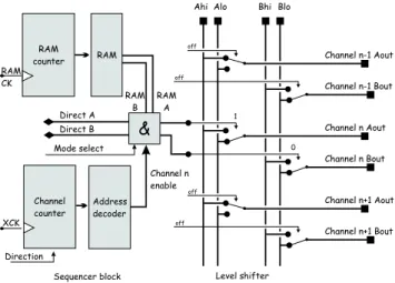
The SWITCHER II is a 64 channel, dual output, high voltage switching circuit manufactured in an AMS high voltage CMOS process. It has been designed for the purpose of DEPMOSFET matrix readout. Figure 5 shows a simplified block diagram of the SWITCHER II IC. The IC consist of a digital control part, a sequencer block and a high voltage levelshifter part. The IC provides two outputs for every channel, theAand theB port. Each port can be switched between two externally applied voltages, Ahi and Alow, and Bhi and Blow respectively.
The voltages can take any value between the positive and negative analog supply rails,V DDAandGN DA. The total voltage difference can be as large as 20 V.
Figure 5. Simplified block diagram of the SWITCHER II IC. The channel selection is done by the channel counter.
Depending on the configuration, the state, active or inactive, of the two channel outputs is determined either by the content of the integrated sequencer RAM or by the state of the so-calleddirectpins. The outputs of non-selected channels are ininactive-condition.
The channel selection is done using thechannel counter, which selects the individual channels consecutively. If a channel is selected, the state of the output ports will be defined by the state of either two discrete input pins, or by the content of the built-in sequencer RAM cells. Various operation modes allow for flexible timing of the switch processes. The polarity of the output ports, i.e. the assignment of the active and inactivestate to the voltages, is defined in the port-individual configuration. If a channel is not selected, its output ports are kept in inactivecondition. Additionally, a number of configuration registers can be used to define the behavior after reset or startup, the sequence, in which the channels are selected and the levelshifter bias currents.
The IC provides facilities to integrate a number of SWITCHER ICs to a daisy chain both for operation, for instance in a case where larger sensor arrays are to be read out, and for configuration, which allows to reduce the number of digital signals for configuration to minimum extend.
On a readout hybrid, two SWITCHER ICs are operated on a single hybrid. Configuration of both SWITCHER ICs happens in a single daisy chain. To ease timing and synchronization of the different ICs, both switchers are operated in direct mode. Switcher #1 generates clearand cleargate voltages, switcher # 2 generates only the gate voltages. An example for typical operation and supply voltages of such a switcher group is shown in figure 6. The clear behavior of DEPMOSFET structures with respect to voltage levels, sequence and timing of clear voltage pulses has been studied on single pixel structures11 and the parameter window where complete clear is possible has been determined. A schematic example for clear timing is shown in figure 6. No limitations in terms of switching speed of the SWITCHER ICs have been encountered so far. Thegatevoltage is active all the time the channel is selected. The signals samples are taken before, the baseline samples right after the clear. The overall clear process has been found to be complete even for a duration as short as 30 ns.
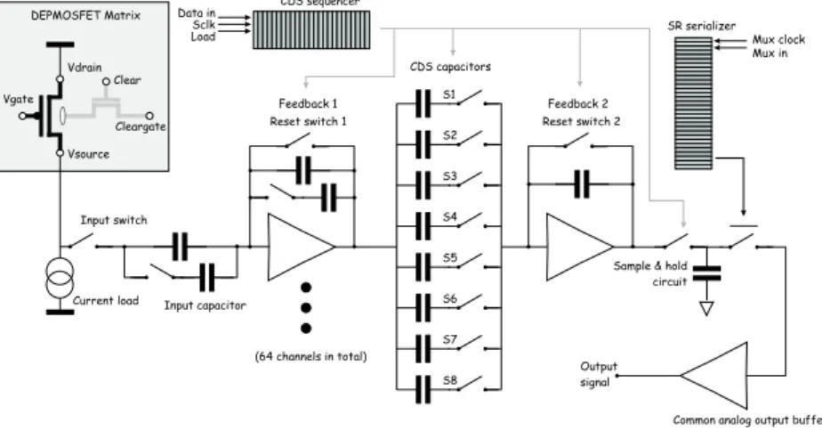
The CAMEX (Charge Amplifier MultiplEXer) 64 G is a 64 channel parallel voltage amplifier with an 8 fold correlated double sampling stage and serial analog readout. It is a variant of the CAMEX family,13 which has been adapted to the requirements of DEPMOSFET pixel readout. It has a PMOS current source integrated in every channel for proper biasing of the source-follower operated pixel columns. Figure 7 shows a simplified schematic of a single CAMEX 64 G channel.
The gain of the CAMEX is defined by the ratio in front of and in the feedback of the two amplifying stages, which can be changed to adapt the dynamic range of the system to different kinds of signals. The maximum gain value of the CAMEX has been measured to be≈120.
The timing of the various switch processes during CDS is generated by a build-in shift register sequencer, the CDS sequencer. It can be programmed arbitrarily allowing for very flexible readout schemes of the device pixels.
The analog signal voltage information is stored on the sample and hold capacitor at the end of the CDS process
Figure 6. Example for SWITCHER voltage settings (left, in volt) and operation indirectoperation mode (right) for a system consisting of two ICs as needed for DEMOSFET matrix readout. The digital part floating with respect to the analog supplies allows for operation of both ICs from a single supply with a common ground. One SWITCHER provides clear and cleargate voltages, the second one only the gate voltage. The XCK signal increments the channel counter. If a channel is no longer selected, all output port voltages return to their inactivelevel. Here, clear and cleargate are active high, the gate voltage is active low.
Figure 7.Simplified channel schematic of the CAMEX 64 G used for DEPMOSFET matrix readout. Every channel has an integrated PMOS current source to bias source follower operation of the pixel columns and an 8-fold-CDS stage with sample and hold. CDS circuitry and S&H are operated by an integrated shift register sequencer, theCDS sequencer, which can hold arbitrary sampling sequences. The nominal gain value of 160 can be changed by adding additional capacitors at the first sampling stage. While the sampling takes place in parallel, readout is done serially using a shift register serializer circuit, which operates independent from the CDS sequencer and multiplexes the sampled voltages to the input of the analog output buffer.
and is read out using a serializer circuit, which operates independently from the CDS sequencer. Usually, readout of the voltage information of a channel takes place in parallel to the CDS process of the next channel to increase system speed. The CAMEX sequencer can be operated at SCLK speeds of up to 10 MHz, the influence of sequencer speed, CAMEX amplifier bandwidth and overall integration time on the system noise are discussed elsewhere.14 At the moment, the minimum processing time for one row is about 12 µs.
4. PERIPHERAL READOUT SYSTEM
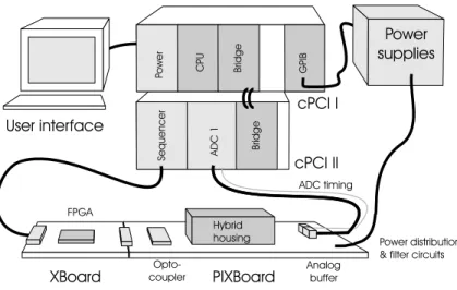
Figure 8 shows a simplified schematic overview over the peripheral readout system. The setup is controlled by
Figure 8. Simplified schematic overview about the system setup. A cPCI CPU controls the sequencer card and the ADC card responsible for data acquisition. The control sequence is transferred via the XBoard digital interface to the PIXBoard, which holds the hybrid inside a light-tight HF shielding box and which performs galvanic decoupling, level shifting, bias generation and distribution and filtering for the various operation voltages. The analog output signals of the hybrids are transferred via an analog buffer to the ADC card, which performs formatting and digitization of the data.
The ADC sample timing is also provided by the sequencer card.
a cPCI CPU running the Windows XP operating system. All digital signals required by the readout system are generated by the sequencer, which is a commercially available NU-DAQ 7300 cPCI sequencer card manufactured by ADLink. The card is used in a configuration, where it provides a 16 track TTL output pattern generator, which is capable of a maximum output frequency of 20 MHz. Additionally, an interface for the implementation of a software controlled slow control and configuration protocol is provided.
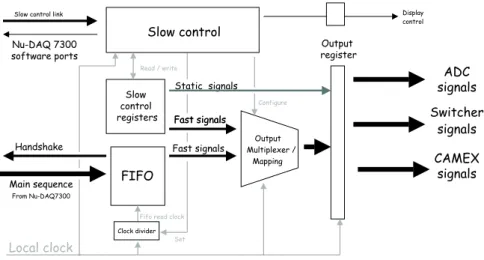
An additional digital interface, the XBoard, was inserted between sequencer and hybrid. The XBoard (XILINX- Board) is a multi-purpose digital interface card holding a XILINX Spartan II FGA. The XBoard FPGA config- uration for the DEMOSFET matrix readout setup was designed to overcome several limitations of the NU-DAQ sequencer card and to provide additional flexibility in readout timing. A simplified block diagram of the XBoard configuration is shown in figure 9.
The XBoard is responsible for configuration and slow control; configuration and programming of, for instance, the sequencers of both switchers and CAMEX, is done with the implemented slow control. The XBoard re- distributes sequencer signals, and as the number of sequencer channels provided is limited, additional signals, statical during operation, can be set via slow control. Also, additional signals can be derived from the pattern stream. The XBoard also resynchronizes the signals, the output frequency of the sequence behind the XBoard FPGA can be set to arbitrary values, and additional integration time can be introduced ad libitum by pausing sequence execution for adjustable time intervals.
The XBoard generated signals are transferred to the so-called PIXBoard (PIXel Board), which decouples gal- vanically from XBoard and sequencer card via a bench of optocouplers. The PIXBoard holds the readout hybrid within an electrically shielded, light-tight housing. The digital signals dedicated to the readout hybrid are con- verted to the appropriate signal standard and distributed to the corresponding pins. The ADC clock and timing control signals are transferred to the ADC timing connector. The PIXBoard also distributes all supply and bias voltages and currents to the ICs and the sensor on the readout hybrid. For this purpose, various filter circuits and biaas generators are present. Finally, the PIXBoard provides digital monitor output for surveillance of system operation as well as analog output buffers for the transmission of the analog output of the CAMEX to the ADC.
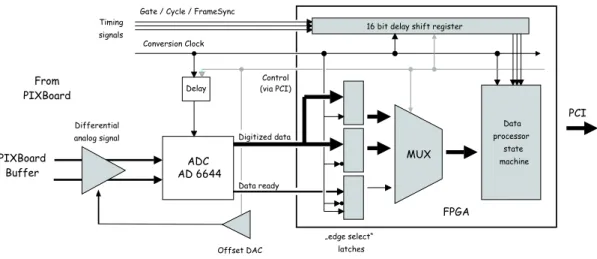
The ADC board is designed for acquisition of DEPMOSFET matrix data with high frequency. It consists of a commercially available cPCI base board, holding an PCI bridge IC and an FPGA with an attached, custom made ADC piggy-back. A block diagram of the ADC-FPGA is shown in figure 10. Main focus was put on correct signal sample timing of the ADC signals and on proper synchronization of ADC output and FPGA
Figure 9.Simplified block diagram of the XBoard FPGA configuration. The local clock, used for resynchronization, can be sourced either from an external clock generator or by the on-board PLL. Due to the handshake mechanism, the signal output frequency can be set to arbitrary values below the maximum output frequency of the pattern generator, which currently is 20 MHz. The slow control block controls the assignment of the static output signals and the configuration of the output multiplexer and the front end ICs of the hybrid.
input. Various ADC control signals allow for storage of data in a frame-compatible format. The ADC used is the AD 6644, which is capable of a maximum digitization speed of 66 MHz. The AD 6644 has 14 bit resolution;
integrated on the ADC piggy-back an effective resolution of 11.7 bit was measured. An integrated offset DAC allows optimum usage of the ADC dynamic range, and several delay stages allow for precise setting of ADC sample timing. Once transferred to the FPGA, the data is transferred to the PCI main memory via fast DMA transfer. The system is capable to cope with a data rate of 40 MByte/s. To avoid interference from mainly the CPU, NU-DAQ sequencer and ADC card are located in a separate cPCI rack. A cPCI-GPIB interface permits control of the system power supplies. Control over ADC card and sequencer is possible using two independent C++ applications.
5. FIRST RESULTS
The system described in the previous sections is operational. Tests of various readout hybrids are in progress. For the analysis of the acquired data it is made use of the HLL-SAS (HLL- Standard Analysis Software) framework, which was originally developed for analysis of data acquired by fully depleted PN-CCDs. After adding some additional pixel related tasks, the HLL-SAS turned out to be a powerful and versatile tool for DEPMOSFET readout hybrid data analysis.
During data analysis, data files are read and, applying a simple threshold algorithm, the noise and offset values of the different pixels are determined together with common mode fluctuations. Then, photon event patterns are detected from the corrected data to recover split events yielding a pulse height spectrum, which is separated according to event patterns. In the third step, photon events identified as singles, i.e. all charge was collected within one pixel, are used to calculate the energy calibration, corresponding to an individual gain value for every pixel. This yields the energy spectrum. The energy resolution of the system is calculated from the energy spectrum of the singles. Additional analysis tasks provide data on the charge splitting behavior, about the linearity of the system and the stability in time.
In the following, selected results from an example dataset taken from hybrid #6 is presented. The hybrid is equipped with a depletion mode device with one metal layer and the FET drain in the center of the respective pixel. For devices with only one metal layer, the current flowing in the source column causes a voltage drop, which can lead to a row-variation of certain parameters, so the transistors have to be operated at low currents.
If the transistor drain is in the center of the pixel, the charge collection of the device is improved. The device was illuminated with an55Fe source for a temperature of -40◦ C with a frame rate of 300 Hz, corresponding to
Figure 10. Block diagram of the ADC module. The differential analog data arriving from the PIXBoard drivers are shifted by an adjustable offset before digitization. The ADC conversion clock is derived from the ADC timing clock generated by the XBoard by an adjustable delay for a more precise setting of sample timing. Synchronization between ADC input and FPGA output is done by a 16 tap pipeline delay to account for ADC-internal delays and by an clock- edge-selective input multiplexer. Once transferred to the FPGA, formatting data generated by the ADC timing signals is added to the data, which is then transferred to PCI main memory using fast DMA.
a single row processing time of 30 µs. The energy resolution is determined by considering both the noise peak information and the FWHM of the Kα-peak.
5.1. Offset and noise distributions
Offset and noise distributions of Hybrid #6 are shown in figure 11. Offset variation is due to spatial variations in leakage currents, gain variations of the pixels leading to a different response to leakage current, voltage drop along the source lines and channel variations in CAMEX gain. From the offset distribution it can be seen that the major contribution comes from variation in CAMEX channel gain, leading to a column dependence of the offset values. However, the measured width of the offset variation is at the order of 100 ADU, which is below 1% of the dynamic range of the ADC and thus tolerable.
The noise is distributed homogeneously over the matrix; the mean value is about 16 ADU, which, regarding the energy calibration information (see figure 13), yields an equivalent noise charge of 4.4 electrons.
5.2. Pulse height spectra
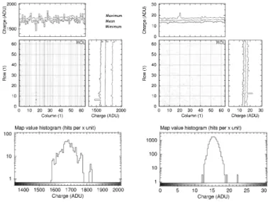
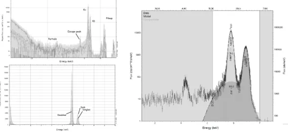
Figure 12 shows the raw pulseheight distribution (left) acquired from the matrix without any correction applied.
As the gain and offset variations are small compared to the total pulseheights, some of the spectral features can be recognized from the raw spectrum. The event entries at pulseheights more negative than the noise peak are misfit-events, which occur accidentally in the time interval between the clear and the time, the CAMEX finishes taking the signal samples. In contrast to out-of-time events occurring during CCD readout, signals like these cannot be mistaken for real photon signals, and they also only assigned to the pixel of their occurrence. After offset correction and event pattern classification (right), the two55Mn-peaks can be clearly separated.
5.3. Energy calibration
An example for a pixel gain map taken for energy calibration is shown in figure 13. To determine the gain value, a pulseheight spectrum containing only photon events classified as singles are taken. The gain value is determined from the position of the Kα-Peak of the respective spectrum. To obtain a reliable gain calibration for every pixel, about 200-300 entries in the respective calibration pulseheight spectrum are required. The resulting distribution is a superposition of CAMEX gain variation, which yields a column-dependence of the gain, and pixel effects. A slight row dependence can be observed, which is due to the voltage drop along the source line.
The overall gain variation is at the order of 5%.
Figure 11. Offset (left) and noise (right) distributions for hybrid #6. As the offset value strongly depends on the column, the major contribution comes from the variation of CAMEX channel gain. The noise distribution over the matrix is homogeneous. The measured mean noise value corresponds to an ENC of 4.4 electrons.
Figure 12. Pulseheight spectra of an 55-source taken with hybrid #6 before (left, logaritmic scale) and after (right, linear scale) offset and common mode correction were applied. The raw spectrum already shows most of the spectral features; for a clearer separation of Mn-Kαand Mn-Kβpeak an offset correction has to be performed. The Al-Kαis due to an aluminum absorber in front of the source. Additionally, the contributions of different event patterns to the overall spectrum are displayed in the corrected pulseheight spectrum.
Figure 13. Example of a gain map of hybrid #6. For determining the gain values, only photon events recognized as Kα photon with no charge splitting were taken. The gain value was determined from the peak position. The measured gain distribution is a superposition of CAMEX gain variation and variations over the pixel matrix. The overall gain variation is at the order of 5%
Figure 14.Energy spectra (left) obtained from the pulseheight spectrum shown in figure 12 after energy calibration in a double-logarithmic (upper) and a linear (lower) plot. The total energy of split events is reconstructed, the resulting energy spectra are displayed separately. Taking the energy spectrum of single pixel events only (right), the energy resolution at the Kα-peak can be determined to be 136.2 eV FWHM, which corresponds to an equivalent noise charge of 7.4 electrons.
5.4. Spectral resolution
The gain map can be used to perform an energy-calibration of the pulseheights. The resulting energy spectrum is displayed in figure 14. The double-logarithmic plot (upper left) shows that the energy resolutions for pile-up events worsens, due to the limited dynamic range of the CAMEX. The linear plot (lower left) shows, that both Kαand Kβ peak for reconstructed doubles are slightly shifted towards higher energies with respect to the peak positions for singles, which is also an effect of CAMEX nonlinearity. From the singles spectrum (right) a value for the energy resolution can be taken. A fit to the Kαpeak applying a simple model for the background yields a FWHM of 136.2 eV, which, after subtraction of the Fano noise contribution, corresponds to a system noise of 7.4 electrons ENC. The discrepancy to the noise value determined from the noise peak is likely to be due to selection effects during the analysis, the very simple background model and charge collection inefficiencies due to improper pixel biasing.
6. SUMMARY AND OUTLOOK
A readout system for evaluation of XEUS DEPMOSFET prototypes has been set up. First prototype devices were integrated together with front end and control ICs into the system and have been successfully taken into operation. In this very early stage, a system noise of 4.4 electrons ENC has been measured at a temperature of -40◦ C, corresponding to an energy resolution of 16.5 eV at the noise peak and 136.2 eV or 7.4 electrons ENC respectively at the Mn Kα.
Next steps include the evaluation of the different design variants in terms of performance and the optimization of matrix operation parameters. For evaluation of matrix devices, the current setup will be further improved and adapted for operation on a vacuum setup allowing for measurements under vacuum at liquid nitrogen temperature.
A second prototype production with a different technology allowing for two metal layers is on the way and will be finished soon, which overcomes the problems of finite source resistance and is expected to allow for an efficient clear for all pixel designs. Additionally, an improved CAMEX version will allow for more sophisticated readout modes and better noise characteristics.
REFERENCES
1. J. Kemmer and G. Lutz, “New detector concepts,”Nucl. Instr. and Meth. A253, p. 356, 1987.
2. J. Kemmer, G. Lutz, U. Prechtel, K. Schuster, M. Sterzik, L. Strueder, and T. Ziemann, “Experimental verification of a new detector concept,”Nucl. Instr. and Meth. A288, p. 92, 1990.
3. P. Klein, G. Cesura, P. Fischer, G. Lutz, W. Neeser, R. Richter, and N. Wermes, “Study of a depjfet pixel matrix with continuous clear mechanism,”Nucl. Instr. and Meth. A392, p. 254, 1997.
4. P. KLein, T. Aurisch, P. Buchholz, P. Fischer, M. Loecker, W. Neeser, L. Strueder, M. Trimpl, J. Ulrici, J. Vocht, and N. Wermes, “A depfet pixel detector system for the use in autoradiography,”Nucl. Instr. and Meth. A454, p. 152, 2000.
5. R. Richter, L. Andricek, P. Fischer, K. Heizinger, P. Lechner, G. Lutz, I. Peric, M. Reiche, G. Schaller, M. Schnecke, F. Schopper, H. Soltau, L. Strueder, J. Treis, M. Trimpl, J. Ulrici, and N. Wermes, “Design and technology of depfet pixel sensors for linear collider applications,”Nucl. Instr. and Meth. A361, p. 250, 2003.
6. X-ray Evolving Universe Spectroscopy-The XEUS Telescope, The XEUS Telescope Working Group, ESA SP-1253, 2001.
7. X-ray Evolving Universe Spectroscopy-The XEUS Instruments, The XEUS Instrument Working Group, ESA SP-1273, 2003.
8. X-ray Evolving Universe Spectroscopy-The XEUS Science case, The XEUS Astrophysics Working Group, ESA SP-1238, 2000.
9. X-ray Evolving Universe Spectroscopy-The XEUS Mission Summary, The XEUS Steering Commitee, ESA SP-1242, 2000.
10. L. Strueder, G. Hasinger, P. .Holl, P. Lechner, G. Lutz, M. Porro, R. Richter, H. Soltau, and J. Treis, “Xeus wide-field imager: first experimental results with the x-ray active pixel sensor depfet,” in High-Energy Detectors in Astronomy, A. D. Holland, ed.,SPIE proceedings5501, 2003.
11. P. Lechner, K. Heinzinger, G. Lutz, M. Porro, R. H. Richter, G. Schaller, M. Schnecke, F. Schopper, H. Soltau, L. Strueder, and J. Treis, “Depfet integrated amplifiers for x-ray imaging and spectroscopy active pixel sensors,” inHigh-Energy Detectors in Astronomy,SPIE proceedings, 2004.
12. E. Gatti and P. Rehak, “Semiconductor drift chambers-an application of a novel charge transport scheme,”
Nucl. Instr. and Meth. A225, p. 608, 1984.
13. W. Buttler, G. Lutz, V. Liberali, F. Maloberti, P. Manfredi, V. Re, and V. Speziali, “Evolution in the criteria that underlie the design of a monolithic preamplifier system for microstrip detectors,”Nucl. Instr.
and Meth. A288, p. 140, 1997.
14. N. Hoernel, S. Herrmann, and M. Porro, “Filter performance of a multiple correlated double sampling system with finite reset,” IEEE transactions on circuits and systems II: Analog and Digital Signal Processing(In preparation).