TECHNISCHE UNIVERSITÄT MÜNCHEN
Max-Planck-Institut für Physik (Werner-Heisenberg-Institut)
Development of thin sensors and a novel interconnection technology for the upgrade
of the ATLAS pixel system
Michael Beimforde
Vollständiger Abdruck der von der Fakultät für Physik der Technischen Universität München zur Erlangung des akademischen Grades eines
Doktors der Naturwissenschaften (Dr. rer. nat.) genehmigten Dissertation.
Vorsitzender: Univ.-Prof. Dr. A. J. Buras Prüfer der Dissertation:
1. Hon.-Prof. Dr. S. Bethke 2. Univ.-Prof. Dr. St. Paul
Die Dissertation wurde am 22.06.2010 bei der Technischen Universität München
eingereicht und durch die Fakultät für Physik am 19.07.2010 angenommen.
Abstract
To extend the discovery potential of the experiments at the LHC accelerator a two phase luminosity upgrade towards the super LHC (sLHC) with a maximum instantaneous luminosity of 10 35 /cm 2 s 1 is planned. Retaining the reconstruction efficiency and spatial resolution of the ATLAS tracking detector at the sLHC, new pixel modules have to be developed that have a higher granularity, can be placed closer to the interaction point, and allow for a cost-efficient coverage of a larger pixel detector volume compared to the present one. The reduced distance to the interaction point calls for more compact modules that have to be radiation hard to supply a sufficient charge collection efficiency up to an integrated particle fluence equivalent to that of (1 − 2) · 10 16 1 MeV-neutrons per square centimeter ( n eq /cm 2 ).
Within this thesis a new module concept was partially realised and evaluated for the operation within an ATLAS pixel detector at the sLHC. This module concept utilizes a novel thin sensor production process for thin n-in-p silicon sensors which potentially allow for a higher radiation hardness at a reduced cost. Furthermore, the new 3D- integration technology ICV-SLID is explored which will allow for increasing the active area of the modules from 71% to about 90% and hence, for employing the modules in the innermost layer of the upgraded ATLAS pixel detector.
A semiconductor simulation and measurements of irradiated test sensors are used to optimize the implantation parameters for the inter-pixel isolation of the thin sensors.
These reduce the crosstalk between the pixel channels and should allow for operating the sensors during the whole runtime of the experiment without causing junction break- downs. The characterization of the first production of sensors with active thicknesses of 75 µm and 150 µm proved that thin pixel sensors can be successfully produced with the new process technology. Thin pad sensors with a reduced inactive edge demonstrate that the active sensor area fraction can be increased to fulfill the requirements for the detector upgrades. A subset of sensors, irradiated up to the fluence expected at the sLHC demonstrated that thin sensors show a higher charge collection efficiency than expected from current radiation damage models. First thin diodes equipped with the SLID metallization and first test structures that were connected with SLID indicate that this novel interconnection as part of the ICV-SLID technology could be a suit- able replacement for the present bump-bonding technology. Finally, a new calibration algorithm for the ATLAS pixel readout chips is presented which is used to lower the dis- criminator threshold from 4000 electrons to 2000 electrons, to account for the reduction of the signal size due to radiation damage and the reduced sensor thickness.
Keywords:
ATLAS, Pixel detector, sLHC, 3D-integration, Radiation damage
Zusammenfassung
Um das Entdeckungspotenzial der Experimente am LHC zu erweitern, ist ein mehrstufi- ger Ausbau des Beschleunigers zum super LHC (sLHC) mit einer maximalen instantanen Luminosität von 10 35 /cm 2 s 1 geplant. Zur Erhaltung der Rekonstruktionseffizienz und der Ortsauflösung des ATLAS Spurdetektors am sLHC müssen neue Pixelmodule ent- wickelt werden, die im Vergleich zu den derzeitigen eine höhere Granularität aufweisen, dichter am Wechselwirkungspunkt installiert werden können und ein größeres Volumen kosteneffizient abdecken. Der geringe Abstand zum Wechselwirkungspunkt erzwingt den Bau von kompakteren Modulen, die bis zu einem integrierten Teilchenfluss äquivalent zu dem von (1 − 2) · 10 16 1 MeV-Neutronen pro Quadratzentimeter ( n eq /cm 2 ) eine aus- reichende Signalausbeute gewähleisten.
Im Rahmen der vorliegenden Arbeit wird ein neues Modulkonzept in Teilen verwirk- licht und für den Einsatz im ATLAS Pixeldetektor am sLHC evaluiert. Dieses umfasst mit einem neuartigen Prozess hergestellte gedünnte n-in-p Siliziumsensoren, die eine höhere Strahlenresistenz bei geringeren Herstellungskosten erwarten lassen. Desweite- ren wird das neue 3D-Integrationsverfahren ICV-SLID eingesetzt mit dessen Hilfe der aktive Flächenanteil der Module von 71% auf ca. 90% erhöht werden kann, um den Einsatz in der innersten Lage des zukünftigen Pixeldetektors zu ermöglichen.
Eine Halbleitersimulation und Messungen an bestrahlten Sensoren werden dazu ein- gesetzt, um die Implantationsparameter der Zwischenpixel-Isolation für die dünnen Sen- soren zu optimieren. Diese soll das Übersprechen zwischen den Pixelkanälen und die Entstehung von elektrischen Durchbrüchen während der gesamten Laufzeit des Experi- ments verhindern. Die Charakterisierung der ersten Produktion von Sensoren mit ak- tiven Dicken von 75 µm und 150 µm belegt, dass dünne Pixelsensoren mit dem neuen Verfahren erfolgreich hergestellt werden können. Dünne Dioden mit reduzierten inakti- ven Randbereichen zeigen, dass der aktive Flächenanteil der Sensoren vergrößert werden kann, um sich für die zukünftigen Detektoren zu qualifizieren. Die Untersuchung einer Teilmenge der Sensoren, die bis zu dem am sLHC erwarteten integrierten Teilchenfluss bestrahlt wurden, zeigt, dass die dünnen Sensoren eine höhere Signalausbeute ermög- lichen als es derzeitige Modelle für Strahlenschäden vorhersagen. Desweiteren wird mit einer ersten Produktion von dünnen Dioden, die mit der SLID-Metalisierung versehen wurden, und ersten SLID-Verbindungen gezeigt, dass die neuartige Verbindungstech- nologie des ICV-SLID Integrationsverfahrens einen Ersatz für das derzeitige Bump- Bonding darstellen könnte. Zuletzt wird ein optimierter Kalibrationsalgorithmus des ATLAS Auslesechips vorgestellt, der dazu verwendet wird, die Diskriminatorschwelle von 4000 Elektronen auf 2000 Elektronen zu senken, um die Auslesechips an die durch die Strahlenschäden und die verringerte Sensordicke reduzierten Signalgrößen anzupas- sen.
Schlagwörter:
ATLAS, Pixeldetektor, sLHC, 3D-Integration, Strahlenschäden
Contents
1 Luminosity upgrade plans for the Large Hadron Collider 3
1.1 Physics motivation . . . . 4
1.1.1 Measuring the parameters of the SM Higgs boson . . . . 4
1.1.2 Precision measurements of Standard Model parameters . . . . 5
1.1.3 Physics beyond the Standard Model . . . . 5
1.2 The LHC accelerator and the luminosity upgrade plans . . . . 6
1.2.1 The first LHC collision runs . . . . 6
1.2.2 Upgrade phase 1 - the LINAC4 . . . . 8
1.2.3 Upgrade phase 2 - the sLHC . . . . 10
1.3 The ATLAS detector at the Super LHC . . . . 10
1.3.1 Upgrades of the ATLAS detector components . . . . 13
1.4 The novel MPP pixel module concept . . . . 16
1.4.1 Requirements for a new pixel module . . . . 16
1.4.2 Improvement of the present module concept . . . . 17
2 Pixel sensors and radiation damage 21 2.1 Working principles of silicon pixel sensors . . . . 22
2.1.1 The pn-junction . . . . 23
2.1.2 N-in-p pixel sensors . . . . 25
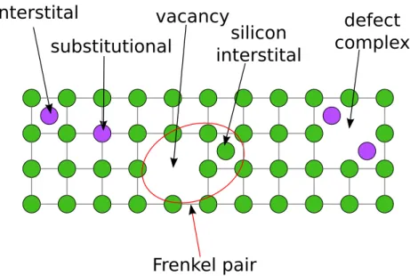
2.2 Crystal defects from irradiation and their implications . . . . 29
2.2.1 Surface defects . . . . 30
2.2.2 Bulk defects . . . . 31
2.2.3 The NIEL scaling hypothesis . . . . 35
2.2.4 Defect annealing . . . . 37
2.3 Approaches towards more radiation tolerant pixel sensors . . . . 38
2.3.1 Thin planar sensors . . . . 39
3 Production and evaluation of thin sensors 41 3.1 Production of thin sensors . . . . 42
3.1.1 The HLL thin sensor production process . . . . 42
3.1.2 Thin FZ sensor production overview . . . . 44
v
3.1.3 Epitaxial thin sensor production . . . . 48
3.2 Simulations of p-spray implant parameters . . . . 50
3.2.1 Semiconductor device simulations with DIOS . . . . 51
3.2.2 Simulation of the potential and electric field distribution . . . . . 55
3.2.3 Simulation results . . . . 57
3.3 Measurements of low dose inter-strip isolations . . . . 64
3.3.1 Sensors under test . . . . 65
3.3.2 Experimental setup . . . . 65
3.3.3 Inter-strip isolation before and after X-ray irradiation . . . . 66
3.3.4 Final choice of production parameters . . . . 69
3.4 Electrical characterization of thin sensors . . . . 70
3.4.1 Initial characterization . . . . 71
3.4.2 Slim guard-ring studies . . . . 79
3.4.3 Characteristics of irradiated thin sensors . . . . 82
3.4.4 Epitaxial sensors . . . . 87
3.5 Charge collection efficiency - simulation and measurements . . . . 91
3.5.1 Charge collection efficiency simulation . . . . 91
3.5.2 Simulation results . . . . 93
3.5.3 Charge collection measurements . . . . 97
3.5.4 The Alibava readout chain . . . . 99
3.5.5 The data taking procedure . . . 101
3.5.6 Results of the charge collection measurements . . . 105
3.5.7 Interpretation of the results . . . 110
3.6 Conclusions . . . 111
4 3D-integration technology for future pixel modules 113 4.1 Solid-Liquid InterDiffusion and Inter-Chip Vias . . . 114
4.1.1 Solid-Liquid InterDiffusion . . . 115
4.1.2 IZM Inter-Chip Vias . . . 117
4.2 Influence of the SLID process on silicon sensors . . . 119
4.3 Efficiency and alignment precision of the SLID interconnection . . . 122
4.3.1 Wafer-to-wafer interconnection . . . 125
4.3.2 Chip-to-wafer interconnection . . . 127
4.4 ICV-SLID for a single-chip demonstrator module . . . 129
4.5 Conclusions . . . 130
5 Optimization of the ATLAS FE-I3 readout chip for small signals 133 5.1 Operation of the FE-I3 . . . 134
5.1.1 The FE-I3 readout chip . . . 135
5.2 The FE-I3 tuning procedure . . . 138
5.2.1 The modified tuning procedure . . . 140
vi
5.3 Tuning results . . . 140
5.3.1 Discriminator threshold and noise . . . 140
5.3.2 Time over threshold . . . 143
5.3.3 Crosstalk . . . 143
5.3.4 Investigations of correlated noise patterns at low thresholds . . . . 144
5.4 Conclusion . . . 145
6 Conclusion and outlook 147
Bibliography 157
vii
viii
Overview
The Large Hadron Collider (LHC) will reach a maximum instantaneous luminosity of 10 34 /cm 2 s leading to an average of 25 proton-proton collisions per bunch crossing and creating a total of around 1000 tracks in the ATLAS inner detector every 25 ns. Already before the start of the LHC, the planning for a two phase luminosity-upgrade program had been started targeting a peak luminosity of 2.3·10 34 /cm 2 s after the phase 1 and up to 10 35 /cm 2 s after the phase 2 upgrade to the super LHC (sLHC). For both collider upgrade phases, also upgrades of the ATLAS pixel detector are needed to allow for efficient tracking despite the increased track multiplicity and the radiation damage caused by secondary particles.
For the phase 1 upgrade an additional innermost pixel layer will be inserted into the present pixel detector which will have suffered from radiation damage. With a reduced instrumentation radius and pixel size of the new layer, the full tracking performance of the present device is planned to be recovered. For the phase 2 upgrade, the complete ATLAS inner detector is planned to be replaced with a new silicon tracking detector also covering the volume of the present gas-based transition radiation tracker. In this scenario the pixel detector will have a smaller inner- and a larger outer radius compared to the present layout. This calls for very compact and also inexpensive pixel modules to efficiently populate the whole foreseen pixel detector volume at affordable cost.
Especially in the innermost tracking layers of the pixel detector, where the track density is very high, the interaction of high energetic particles with the silicon sensors leads to a considerable damaging of the crystal lattice structure. Normalized to the radiation damage of 1 MeV neutrons (n eq ), modules of the innermost layer of the ATLAS pixel detector at the sLHC will be exposed to an integrated radiation dose of (1 − 2) · 10 16 n eq /cm 2 . The resulting radiation damage in the pixel sensors leads to high leakage currents and a reduction of the signal size. The most demanding challenge of the module upgrades is to develop sensors and readout electronics that allow for an operation with a high signal efficiency in this extreme environment.
Within this thesis, the development towards a novel ATLAS pixel module is presented
that is proposed by the Max-Planck-Institut für Physik (MPP). The module will include
the new 3D-interconnection technology ICV-SLID and a reduced guard-ring structure
for the sensors to reach a higher active fraction and compactness to fulfill the criteria
2
for the innermost pixel layer of the upgrades of the pixel detector. To still use the more efficient electron readout, the sensors will use the n-in-p doping concept while allowing to reduce the number of processing steps during the sensors fabrication compared to the present n-in-n sensors. This will lower the production costs to allow for large area detectors. Furthermore, the sensors will be produced with a new production process for thin sensors which was developed at the semiconductor laboratory HLL of the Max- Planck-Gesellschaft (MPG). Thin sensors are expected to deliver a higher signal after large irradiation doses compared to sensors of standard thickness due to their different electric field configurations. Nevertheless, the signal sizes of the sensors at the sLHC are expected to decrease due to the radiations damage. Therefore, to allow for successful module operation at high signal to noise ratios, the threshold of the pixel readout chips has to be lowered.
This thesis is organized as follows: Chapter 1 gives a short summary of the physics
prospects of the sLHC and introduces the phase 1 and phase 2 upgrade plans of the LHC
collider. Chapter 2 describes the basic functionality of semiconductor sensors as well as
the processes leading to radiation damage and highlights the benefits of the novel MPP
module concept for the operation at the sLHC. In Chap. 3, the results from a semicon-
ductor simulation and measurements of pre-production sensors are presented that have
been conducted to define the most promising implant parameters applied for the main
thin sensor production. The characterization of the first thin pixel and strip sensors
from the main production is shown and especially the results of measurements of the
signal size before and after proton irradiation are presented. Measurements of diodes
with a reduced guard-ring structure indicate that a decrease of the inactive edge to less
than 500 µm can be achieved. Chapter 4 summarizes the results obtained so far towards
the use of the ICV-SLID 3D-integration technology. A proof of principle for the com-
patibility of this technology with semiconductor sensors is given and the interconnection
efficiency is characterized with test structures. Future steps of the ongoing R&D are
outlined. Chapter 5 recapitulates the most important results on the optimization of the
discriminator threshold of the present ATLAS readout chips with a modified calibration
algorithm. At the end, a summary concludes the results of this thesis.
Chapter 1
Luminosity upgrade plans for the Large Hadron Collider
"What I cannot create, I do not understand."
R. Feynman, written at his blackboard at the time of his death in 1988 [1]
The Large Hadron Collider (LHC), located at the Conseil Européen pour la Recherche Nucléaire (CERN) [2] near Geneva, is the largest and most powerful proton collider in existence today. Colliding protons at a foreseen center of mass energy of 14 TeV, ele- mentary particles are created and used to study the physics of the fundamental building blocks of nature and their interactions. In an alternative operation mode the LHC ac- celerator can also be used for lead-lead heavy ion collisions at an energy of 2.76 TeV per nucleon or 574 TeV per ion, surpassing the energies reached at the Relativistic Heavy Ion Collider (RHIC) [3] at the Brookhaven National Laboratory by almost a factor of 30. Detailed reviews of the physics opportunities at the LHC can be e.g. found in [4, 5].
With a nominal luminosity of 10 34 /cm 2 s 1 the LHC will surpass the peak luminosity
of the Tevatron collider at the Fermilab by over a factor of 30 [6]. The luminosity in-
tegrated over the first 5 years of LHC operation time is expected to reach 300 fb −1 [7],
compared to the 8 fb −1 produced during the Tevatron Run-II so far [8]. Nevertheless,
an upgrade of the LHC luminosity is currently being planned, targeting a peak value
of 10 35 /cm 2 s 1 and an integrated luminosity of up to 3000 fb −1 [7] at the so called Su-
per LHC or sLHC. The motivation behind this upgrade is to extend the measurement
precision of particle parameters as well as the discovery potential for physics beyond
the Standard Model (SM) of elementary particle physics. As major hardware upgrades
of the accelerator and detectors have to be carried out to increase the luminosity by
a factor of ten, a prolonged operation shutdown period is needed. This is planned to
4 Chapter 1. Luminosity upgrade plans for the Large Hadron Collider coincide with the mandatory shutdown after about 10 years of data taking at the nom- inal luminosity which is needed to replace detector components and focussing magnets which will suffer from radiation damage [9].
In this chapter, Sec. 1.1 gives a short introduction to the physics cases that can be investigated with a ten-fold luminosity at the sLHC. Section 1.2 introduces the LHC accelerator complex and possible scenarios for reaching the targeted peak luminosity in a two step upgrade. In Sec. 1.3, the ATLAS detector is briefly introduced with an explicit focus on the sLHC upgrade strategies for the different sub-detector components. Finally, Sec. 1.4 gives an overview of the pixel module concept proposed by the Max-Planck- Institut für Physik (MPP) for use in the ATLAS detector during the sLHC operation.
This novel module concept, being the main research target of the presented thesis, is expected to allow for the production of radiation hard, very compact, and cost-effective pixel modules for large scale tracking detectors.
1.1 Physics motivation
There are several physics cases that call for a luminosity upgrade of the present LHC accelerator. Some of them are already foreseeable at this point in time, while others depend much on the physics actually realized in nature and probed by the LHC. In general, the discovery reach of the experiments at the sLHC accelerator can be extended to higher particle masses by (20 − 30)%, and the statistical error halving time, which will have reached around 5 years at the time of the foreseen upgrade, can be reduced with the increased luminosity [9]. More specific examples of measurements which profit from the higher luminosity at the sLHC are listed in the following.
1.1.1 Measuring the parameters of the SM Higgs boson
The Higgs boson was proposed in 1964 [10, 11, 12] to explain the origin of the masses of the W and Z bosons via the Higgs-Mechanism. Also the massive fermions of the SM could acquire their mass by coupling to the Higgs field via the Yukawa coupling.
The Higgs boson is the last particle of the SM which has not been discovered yet.
The current upper limit for the Higgs boson mass in the SM, deduced from precision measurements of the W-boson and top quark masses, is m H ≤ 157 GeV/c 2 at 95%
CL [13]. By direct searches for the Higgs boson, the LEP experiments have set a lower limit of m H ≥ 114.4 GeV/c 2 on the Higgs mass also at 95% CL. Recently the mass range of 163 GeV/c 2 < m H < 166 GeV/c 2 was excluded at a 95% CL by experiments conducted at the Tevatron [14]. Taking into account the exclusion limits from the direct searches, the upper limit for a SM Higgs is currently m H ≤ 186 GeV/c 2 [13].
For the multi-purpose experiments ATLAS [15, 16] and CMS [17] at the LHC, search
strategies have been established over the last years to be sensitive to Higgs boson sig-
1.1. Physics motivation 5 natures over a large mass range up to m H = 1 TeV/c 2 , also covering the mass range predicted for a supersymmetric Higgs boson [18, 19]. If the Higgs boson has been dis- covered, its parameters have to be precisely measured. These include the mass, the spin, the CP-quantum numbers, and the couplings to itself as well as to other fermions and bosons. The Higgs boson mass can be measured over a wide mass range using the elec- tromagnetic γγ or 4-lepton final states. The spin and the CP quantum numbers can be deduced by the angular distribution of the four leptons in the decay H → ZZ → 4l [20].
Since the coupling strengths cannot be measured directly, the couplings to bosons and fermions will be normalized to the H → WW → lνlν rates [21]. At the sLHC the rela- tive couplings of fermions and bosons to the Higgs are expected to be measured at an accuracy of (10 − 20)%, an improvement by a factor of two compared to the LHC [9].
Furthermore, new rare decay channels will become accessible including H → µµ and H → Zγ [22].
To fully prove or disprove the Higgs mechanism, the Higgs self-coupling strength λ HHH has to be measured to deduce the shape of the Higgs potential. Due to the limited production rates, measuring the Higgs self-coupling is not possible at the LHC. The self-coupling strength enters in the Higgs pair-production and it has been suggested to look for HH → WW WW decays at the sLHC if m H > 140 GeV [23].
1.1.2 Precision measurements of Standard Model parameters
At the end of the LHC operation, most measurements of SM parameters will not be limited by the statistical uncertainties, but rather by the systematic uncertainties of the Monte Carlo simulations, the detector performance, and the physics models. However, there are measurements of rare processes in the SM that benefit from the increased statistics collected at the sLHC. One example are the rare top quark decays which are mostly believed to be beyond the reach of the LHC. There is a class of theories beyond the SM that predicts branching ratios of top quark decays by flavor changing neutral currents (t → qγ, t → qZ, and t → qg where q = u, c) of 10 −5 − 10 −6 [22]. Especially for the decay process t → qZ, the sensitivity depends almost linearly on the luminosity and therefore can be improved significantly at the sLHC. Nevertheless, to reach this enhanced sensitivity the performance of identifying b-quarks, i.e. the b-tagging, must be kept at the same level as for the present detectors. This poses a strong challenge to the future detectors which will have to cope with a much higher track density.
1.1.3 Physics beyond the Standard Model
The LHC will be the first accelerator to probe physics processes at energies well above
the electroweak symmetry breaking scale. Several Beyond-the-Standard-Model (BSM)
models exist that could already be probed at the LHC. These are for example SUper
SYmmetry (SUSY), extra dimensions, technicolor and leptoquarks. Reviews can be
6 Chapter 1. Luminosity upgrade plans for the Large Hadron Collider found, e.g. in [24, 25, 26, 27] and references therein. The physics case of the sLHC strongly depends on the physics discovered at the LHC, but the sLHC will in general be able to extend the discovery potential for the given models to higher masses. Fur- thermore, the sensitivity of the rate-limited processes will be increased giving excess to higher precision measurements at the highest energies.
If for example SUSY is discovered at the LHC, the masses and the model parameters will have to be measured. Depending on the energy scale where SUSY will reveal itself, this will not be possible at the LHC. The precise measurement of SUSY particles requires in most cases the selection of exclusive decay modes containing leptons or b-jets, being in some cases rate-limited. For these, the sLHC will provide an improvement in the statistical uncertainties if the detector, especially the trackers will show the same tracking performance as the present ones. In the case of no observation of SUSY particles at the LHC, the upgrade to the sLHC can extend the discovery reach by about 0.5 TeV up to 3.0 TeV [9].
1.2 The LHC accelerator and the luminosity upgrade plans
The present accelerator complex of the LHC is shown in Fig. 1.1. Only one of the two LINear ACcelerators (LINACs) can be used at a time to either introduce protons or heavy ions into the accelerator system. In the case of using the LHC as a proton accelerator, the LINAC2 accelerates the protons up to an kinetic energy of 50 MeV and injects them into the accelerator chain of the Proton Synchrotron Booster (PSB, 1.4 GeV), the Proton Synchrotron (PS, 26 GeV), and the Super Proton Synchrotron (SPS, 450 GeV). From the SPS the protons are injected into the main LHC accelerator.
Here, for the first time they are circulating in opposing directions and thus, can be collided at the four interaction points at the experiments ATLAS, CMS, ALICE [28], and LHCb [29]. In the heavy ion runs, the linear accelerator LINAC3 is used to inject the lead atoms with an energy of 4.2 MeV per nucleon into the Low Energy Ion Ring (LEIR). From here, they follow the same acceleration process through the PS and SPS into the LHC which they enter with an initial energy of 177 GeV per nucleon.
1.2.1 The first LHC collision runs
After the first LHC startup in late 2008 and the following shutdown due to a technical
failure, the collider was successfully repaired and restarted in 2009. Starting with first
injection tests in October of that year, the LHC circulated first proton beams in Novem-
ber when also first collisions were seen. On the 30 th of November, both proton beams
were accelerated to 1.18 TeV setting a new world record for proton accelerators. The
first collisions at this record energy were initiated in December and first collision data
1.2. The LHC accelerator and the luminosity upgrade plans 7
Figure 1.1: The LHC accelerator complex [2].
8 Chapter 1. Luminosity upgrade plans for the Large Hadron Collider was taken by all four main experiments. From early 2010, a long physics run has started collecting the first 1 fb −1 with a beam energy of 3.5 TeV. On the 30 th of March, the first collisions and successful physics data taking of all four main experiments at this new record energy set the start of this run which is planned to last up to the end of 2011.
After this, a shutdown will follow to prepare the accelerator for the nominal beam energy of 7 TeV. At this energy it is planned to reach a maximum instantaneous luminosity of 10 34 /cm 2 s 1 . The LHC will be operated with these parameters for several years, until an integrated luminosity of about 100 fb −1 is collected in 2014 to 2015 [30]. At this point, a first longer shutdown is planned to start with the first of the two luminosity upgrade phases.
1.2.2 Upgrade phase 1 - the LINAC4
The maximum luminosity for ideal head-on collision L head of the LHC accelerator de- pends on the beam current I, the beam brightness B , and the beam geometry at the interaction point:
L head = γ
4πβ ∗ · B · I, with γ = 1
p 1 − β 2 and β = v/c. (1.1) Here v is the particle velocity, c the vacuum speed of light, and β ∗ is the beta function at the interaction point [31]. The brightness
B = N b
n (1.2)
depends on the number of protons per bunch N b , and the normalized transverse emit- tance n = βγ. The beam current
I = N b · n b · f rev (1.3)
also depends on the number of protons per bunch, the number of bunches per beam n b , and the revolving frequency f rev of the protons. At the Interaction Points (IPs) located within in the detectors, ideal head-on collisions are not possible, due to the crossing- angle θ c between the beams. This introduces a geometric reduction F of the maximum luminosity leading to
L = L head · F = L head · 1 q
1 + θ 2σ
cσ
∗z. (1.4)
Here, σ ∗ = √
β ∗ is the RMS of the transverse beam size and σ z is the RMS of the bunch
length.
1.2. The LHC accelerator and the luminosity upgrade plans 9
LINAC 2
LEIR
LINAC 3
Figure 1.2: The new LINAC4 injector and the present PSB-PS accelerator system [33].
For the planned luminosity upgrades, several of these parameters will be optimized.
In the first phase to extend the physics reach of the LHC, the luminosity is going to be increased by replacing the LINAC2 with a new proton injector. This approach is followed since the main bottleneck for the current luminosity is the beam brightness, which is limited by space charge effects at the injection of protons from the LINAC2 into the PSB [30]. Figure 1.2 shows the schematics and the location of the new LINAC4 [32], already being under construction to overcome this problem. It is 100 m long and injects the protons through a transfer line into the PSB. The orientation of the LINAC4 is chosen to allow for a future upgrade to higher energies and direct proton injections into the SPS accelerator.
The LINAC4 will accelerate negatively charged H − -ions instead of protons to a ki- netic energy of 160 MeV. Before the protons are injected into the first ring accelerator, a stripping foil is used to remove the electrons. With this well proven technology and the increased energy, protons can be accumulated in the accelerators at smaller transverse emittances n . For the same number of protons per bunch the LINAC4 will be able to deliver an improvement of the brightness, and thus the luminosity, by a factor of two.
With additional optimizations of the focussing magnets at the experiments, leading to
a reduction of β ∗ , a maximum luminosity of 2.3 · 10 34 /cm 2 s 1 is planned to be reached
with this phase 1 upgrade [9]. Current planning foresees the finishing of the LINAC4
construction and the first delivered protons in 2014 or 2015.
10 Chapter 1. Luminosity upgrade plans for the Large Hadron Collider
(a) FCC (b) LPA
Figure 1.3: The Full Crab Crossing (FCC) scheme and the Large Piwinski Angle (LPA) approach [30].
1.2.3 Upgrade phase 2 - the sLHC
The second upgrade phase towards the sLHC is expected to be carried after around ten years of physics data taking. The primary goal of this upgrade is to increase the luminosity to the maximum value reachable, targeting a ten-fold increase to 10 35 /cm 2 s 1 . This will involve major changes to the beam- and IP parameters. However these have not been finalized so far, since only after gaining experience from the present accelerator operation the best upgrade approach can be assessed.
Nevertheless, two alternative upgrade scenarios are already thought of. Figure 1.3 shows the schematics of these two very different approaches. The first (Fig. 1.3(a)) will involve installing crab cavities [34, 35] close to the IPs. These reduce the effective crossing angle of the bunches to allow for almost head-on collisions, i.e. an effective reduction of θ c and hence, an increase of the geometric reduction factor F closer to 1. The second approach (Fig. 1.3(b)) does not try to decrease the crossing angle, but rather to increase the number of protons per bunch at a constant n . Here it is planned, to increase N b proportional to 1/F so that the product B · F remains constant. Since N b also enters in I, it follows L ∝ N b .
Both of these scenarios involve major rework, especially of the focussing magnets but could be realized with the new LINAC4 injector scheme presented above.
1.3 The ATLAS detector at the Super LHC
With a length of 44 m, a height of 25 m, and a mass of 7000 t, the ATLAS 1 detector (see e.g. [36] and references therein) is the largest detector ever built at a particle collider.
1
ATLAS: A Toroidal LHC ApparatuS
1.3. The ATLAS detector at the Super LHC 11 In Fig. 1.4(a) the main detector components of ATLAS are presented. Each of them is centered around the IP and consists of a cylindrical barrel section with endcaps on each side. Emerging from the collisions in the center of the detector, the secondary particles first pass the different sub-detectors of the inner detector (ID) [37, 38] (Fig. 1.4(b)) residing in a 2 T solenoidal magnetic field. These are the semiconductor pixel detec- tor [39], the SemiConductor Tracker (SCT) (e.g. [40] and references therein), and the Transition Radiation Tracker (TRT) [41]. Both, the pixel detector and the SCT consist of an arrangement of many detector modules, mounted on barrel and endcap support structures. Each of the modules consists of a patterned silicon sensor with attached readout electronics. The detection principle is based on the collection of electron-hole pairs created by ionizing particles in depleted silicon. The TRT consists of straw tubes with a diameter of 4 mm containing a gas mixture and a central gold plated tungsten anode wire. Penetrating particles ionize the gas atoms and the radial electric field con- figuration is used to amplify the drifting charges via avalanche multiplication. Between the straws a polypropylene-polyethylene fiber radiator is placed to cause the emission of transition radiation by penetrating particles. This is mainly used to discriminate between electrons and pions. A total of up to 47 hits are created by charged particles interacting with the ID detector components, most of them in the TRT. They can be assigned to one or several readout channels of the detectors and from this, the initial ver- tex as well as the momentum of the particles can be reconstructed. The pseudo-rapidity
η = − log θ
2
(1.5) with θ being the angle between the beam-axis and the particle momentum, is covered by the ID over a range up to |η| < 2.5.
Outside of the solenoid magnet, the electromagnetic and hadronic sampling calorime- ters follow [42]. The electromagnetic calorimeter is used to detect particle showers from electromagnetically interacting particles. The active material of the electromagnetic calorimeter is liquid argon which is interleaved with lead, used as the absorber material, in an accordion arrangement. The hadronic calorimeter follows the same principle but uses scintillating tiles and iron absorbers in the barrel part. Liquid argon and copper as well as tungsten absorbers are used in the endcap region. The hadronic calorimeter is designed to measure showers from strongly interacting particles, which are generally not stopped in the electromagnetic calorimeter. From the shape of the showers in both calorimeters the energy of the initial incident particle can be determined.
Surrounding the calorimeters, the ATLAS muon spectrometer follows [43]. It is en-
closed in a 4 T toroidal magnetic field, giving ATLAS its name, which is used to bend the
trajectories of the muons, usually not stopped in the calorimeters. The muon spectrom-
eter comprises the Monitored Drift Tubes (MDTs) and the Cathode Strip Chambers
(CSCs) for precision muon tracking. Resistive Plate Chambers (RPC) and Thin Gap
Chambers (TGP) are used for triggering and the later also to gain additional tracking
12 Chapter 1. Luminosity upgrade plans for the Large Hadron Collider
(a)
(b)
Figure 1.4: The ATLAS detector (a) and the barrel part of inner detector (b), both
from [16].
1.3. The ATLAS detector at the Super LHC 13 information in the forward region. The aluminum MDTs with a radius of 30 mm are gas filled and contain a central anode wire to create a radial electric field. Similar to the TRT detection principle, penetrating muons ionize the gas atoms and the generated charges are separated and eventually multiplied close to the anode wire. To increase the spatial resolution of the tubes also the drift time of the charges is determined.
Combining the results from all sub-detector components, most of the particles cre- ated in the collisions can be identified and their initial vertex and energy can be mea- sured. From the presently known particles, neutrinos which are solely weakly interacting manifest as missing energy.
1.3.1 Upgrades of the ATLAS detector components
Increasing the luminosity of the LHC accelerator inevitably leads to additional require- ments for some of the ATLAS sub-detectors. In general, the occupancy of all sub- detectors increases and especially for detectors with very high hit rates, i.e. those located close to the IP and in the high η regions, radiation damage will deteriorate the detector performance. The following discusses the planned upgrades of the individual detector components for the phase 2 upgrade. For the innermost pixel layer, even after the phase 1 upgrade, changes to the pixel detector are foreseen.
Muon system
Most parts of the muon system are far away from the interaction point and thus, are not expected to suffer from radiation damage. However, due to the comparably large area of the readout channels and their dead-time of at least 200 ns, the occupancy can reach more than 30% in most MDTs and CSCs [44]. This high occupancy is mainly caused by the large neutron and photon background stemming from secondary interactions in the calorimeter systems. To reduce the high occupancy in the most affected areas, i.e. especially in the forward direction close to the interaction point, a replacement of the present MDTs and some of the CSCs is planned, using aluminum tubes with a reduced radius of 15 mm. This shortens the maximum drift time from 700 ns to 200 ns and allows for an increase of the maximum hit rate per area by a factor of three. Instead of a three layer-design the thin tubes allow for a six-layer design, doubling the redundancy for reconstructing the muon tracks.
Calorimeters
As for the muon spectrometer, most components of the calorimeter system will not
suffer from radiation damage. The scintillator tiles in the barrel region of the hadronic
calorimeter are sufficiently far away from the IP and the liquid argon calorimeters are
intrinsically radiation hard. However, especially in the forward region, the radiation
14 Chapter 1. Luminosity upgrade plans for the Large Hadron Collider level will be significant and might cause a deterioration of the cold electronics in the Hadronic Endcap Calorimeter (HEC). Therefore, investigations to evaluate the radiation hardness of the electronics as well as research and development towards their upgrade are carried out [45]. Furthermore, especially the liquid argon Forward CALorimeter (FCAL), covering the pseudo-rapidity range of 3.1 < |η| < 5.0 at low z, faces two challenges. The first is the increased build-up of space charges in the active medium leading to a modification of the measured signal size. Even though the gap size between the absorbers filled with the active medium is only 250 µm, current developments aim at reducing this gap size down to 100 µm to decrease the build-up of space charges.
The second challenge, provoked by a ten-fold increase of luminosity is the increased heat load caused by the energy absorbed in the calorimeters. Current simulations fore- see a power dissipation of 400 W/m 2 which would lead to temperatures above the boil- ing point of the liquid argon, considering the current cooling system and operating parameters [46]. Replacing the forward calorimeter modules represents a serious lo- gistical challenge, since it would involve opening the endcap cryostats. Including the re-assembly, this would take up to three years [47], being too long for the anticipated upgrade shutdown. Therefore, new strategies are investigated that involve installing a new calorimeter, which does not need to be cooled, between the IP and the present forward calorimeter. It could be used for additional energy measurements and as a radiation shield, avoiding major upgrades of the present system. However, still under discussion is the availability of space and the impact of such a calorimeter on the ID in terms of increasing occupancy due to back-scattering.
Inner detector
For the sLHC, the upgrade of the ID will pose the highest technical challenge in terms of data processing, track discrimination power, and radiation damage. Already in the early phase of the planning towards the phase 2 LHC upgrade it was evident, that the gas-based TRT cannot cope with a ten-fold increase of the hit rate. Therefore, it was decided by the upgrade steering group [48], that during a complete upgrade of the ID, the TRT will be replaced by silicon based detectors with a much higher granularity.
An initial layout of the new ID has been proposed which is called the strawman,
being a flexible and rearrangeable first approach. Several iterations of this layout have
led to the current version shown in Fig. 1.5, which might still be subject to changes. The
outer part consists of a large volume n-in-p silicon strip detector with modules on five
layers in the barrel region and five endcap discs at each side. In the barrel region, the
outer two layers, spanning over a radial range of 74.3 cm < R < 100.0 cm, will comprise
long-strip sensors with an approximate cell size of 80 µm × 10 cm. The inner three layers
of short-strip sensors with a cell size of 80 µm × 2.5 cm will populate the volume within
38.0 cm < R < 62.2 cm. Each of the modules consists of two sandwiched single-sided
sensors with a small stereo angle to improve on the resolution along the strip direction.
1.3. The ATLAS detector at the Super LHC 15
Figure 1.5: The present strawman layout [48] of the inner detector for the ATLAS detector at the sLHC.
Encompassed by the strip detector, the pixel detector with four barrel layers with radii of 3.7 cm < R < 20.9 cm and five endcap discs is located. The outer two layers will have a pixel cell size of 50 × 250 µm 2 and the inner two of 50× ≤ 200 µm 2 for improved resolution and decreased hit occupancy. Like for the present ID, the strawman layout covers the pseudorapidity range up to |η| = 2.5.
With the replacement of the TRT by silicon sensors and the reduction of the pixel size in the innermost layers, the occupancy can be lowered to allow for efficient operation at the sLHC. However, especially the innermost pixel layers also face radiation damage that will accumulate during the LHC, and even faster, during the sLHC operation. For this reason already coinciding with the LHC phase 1 upgrade, an upgrade of the ATLAS pixel detector is planned. At this point in time the radiation damage is expected to impair the signal efficiency of the sensors in the innermost pixel layer, i.e. the so called b-layer. The shutdown for the LHC phase 1 upgrade is planned to last less than one year, forbidding a complete exchange of the present pixel detector. Therefore, only a new b-layer will be build, that is going to be mounted directly onto a new slimmer beam-pipe and will be slided into the present b-layer [49]. The foreseen mean sensor radius of the new b-layer is R = 3.2 cm. This phase 1 ATLAS pixel detector upgrade is commonly referred to as the Insertable B-Layer or IBL upgrade.
In both upgrade phases the innermost pixel detector layer will be closer to the IP
than the present b-layer, and the luminosity will be higher than the design luminosity
16 Chapter 1. Luminosity upgrade plans for the Large Hadron Collider of the LHC. Therefore, the new pixel modules will have to be optimized for radiation hardness, and compactness to achieve a large live-fraction, i.e. a large ratio of active sensor area to the total area of the modules. In addition, the material budget of the modules has to be reduced as much as possible since the effect of multiple scattering close to the IP significantly decreases the tracking performance. There are several research projects ongoing that try to develop pixel modules that meet the requirements for the IBL and sLHC upgrades. In the following, the pixel module concept developed at the MPP will be presented.
1.4 The novel MPP pixel module concept
In this section the requirements for the pixel modules for the upgrade scenarios and the approach of the MPP to meet these requirements are discussed. The target detector of this research is the ATLAS pixel detector for the sLHC, however, also a sensor production for the IBL upgrade is anticipated. The individual components of the new MPP module concept are described in the following.
1.4.1 Requirements for a new pixel module
Presently, the requirements for a pixel detector at the sLHC are only partly known since some of the effects of high luminosity operation can only be estimated after run- ning the present device at the LHC for some time. One of the key ingredients to a pixel detector close to the IP is the radiation hardness, i.e. the resistance to damages caused by high energetic particles penetrating the detector. Current estimations of the expected integrated fluence Φ eq , scaled to the radiation damage of 1 MeV neutrons per square centimeter ( n eq /cm 2 ), are extracted from a Monte-Carlo simulation [47]. This is presented in Fig. 1.6, as a function of the radial distance from the IP for different values of |z| (measured along the beam-axis with the IP located at z = 0), and assum- ing an integrated luminosity of 3000 fb −1 . Since the innermost pixel layer will likely be placed at a radius of 3 cm < R < 4 cm, it will be exposed to an equivalent fluence of Φ eq ≈ (1 − 2) · 10 16 n eq /cm 2 , depending on the safety factors multiplied to the simulation results.
Apart from the requirements with respect to radiation hardness, the smaller radius
of the innermost pixel, compared to the present ATLAS pixel detector also leads to
additional requirements for the module arrangement. While the layout of the ID for
the sLHC is not fixed yet, the one for the IBL upgrade is strongly restricted due to
the already present pixel detector. The foreseen radius envelope of the new b-layer is
so small that shingling in z, i.e. an overlap of the modules in the direction along the
beam-axis, like in the present detector, is not possible. This restriction is also expected
to hold for the detector for the phase 2 upgrade. If shingling along this direction is
1.4. The novel MPP pixel module concept 17
n /cm eq 2
Figure 1.6: Expected equivalent fluences Φ eq (in n eq /cm 2 ) in the tracking detector at the sLHC as a function of the radial distance from the beam-line [47].
not possible, the active area of the pixel sensors has to extend as far as possible to the module edges perpendicular to the z-axis. The target value for the width of the inactive edge on these two sides is (450 − 500) µm [50], being a reduction of 50% compared to the current sensors.
Another goal that is followed is the reduction of the material budget of the detectors.
Since multiple scattering causes a deterioration of the tracking performance especially in the innermost layers, it is planned to reduce the material budget of the pixel module support structures, the cooling system, and also the detector modules. Apart from the physics requirements, also the monetary aspect has to be considered for such a large scale semiconductor detector. Therefore, a cost optimization is much desired.
1.4.2 Improvement of the present module concept
The present ATLAS pixel module (Fig. 1.7) consists of three layers of active components
and has an area footprint of about 2.0 × 6.3 cm 2 . A 250 µm thick n-in-n silicon pixel
sensor forms the central layer of the module in which the penetrating charged particles
generate the signals. Bump-bonding is used to connect the contact pads of the individual
pixel cells of 50×400 µm 2 to the 46080 input pads of 16 FE-I3 ATLAS readout electronics
chips [51]. In the readout electronics the signals are amplified, digitized, and via wire-
18 Chapter 1. Luminosity upgrade plans for the Large Hadron Collider
Figure 1.7: Technical drawing of the ATLAS pixel module [16].
1.4. The novel MPP pixel module concept 19
(a)
p-substrate
thin readout chip
thin sensor n+
HV
SLID ICV
(b)
Figure 1.8: A schematic view of the present ATLAS pixel module concept (a) in com- parison to the proposed MPP concept (b).
bonds on the cantilever, running along the long side of the modules, transmitted to the uppermost module layer (side-view in Fig. 1.7). The top layer flexible printed circuit board (flex) is glued to the sensor and contains next to several surface mounted devices (SMDs) also the Module Control Chip (MCC), which collects the data from the 16 FE-I3 chips. Over the so called pigtail the data from the MCC is transmitted to the off-detector data acquisition system.
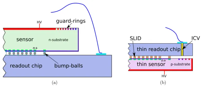
A schematic side view of the long edge of the present ATLAS pixel module is shown in Fig. 1.8(a). Compared to this, the MPP pixel module proposed [52] for the ATLAS pixel detector sLHC is shown in Fig. 1.8(b). It contains several new technologies and optimizations for a higher compactness and increased radiation hardness to meet the requirements for operation at the sLHC:
• Thin sensors: Particle irradiation induces crystal defects in silicon sensors that lead to a reduction of the signal and an increase of the noise contribution. Sensors with a thickness of less than the standard 250 µm are expected to be less affected by the signal reduction processes and therefore more radiation hard. In addition, since the radiation length of the sensors is proportional to their thickness, thin sensors reduce multiple scattering. To explore these advantages of thin sensors, a novel thinning technology, developed at the semiconductor laboratory HLL [53]
of the MPG, is used to produce sensors with a thickness, which can be optimized
for a maximum signal to noise ratio at the expected fluences. The preparations
preceding the production and the results of the first thin pixel sensor production
are presented in Chapter 3.
20 Chapter 1. Luminosity upgrade plans for the Large Hadron Collider
• N-in-p sensor design: The use of an n-in-p sensor design is foreseen (Fig. 1.8(b)).
This allows for less processing steps during the sensor production compared to the present ATLAS n-in-n design since the sensors only need a structured processing on one side. This should lead to a cost reduction, since the processing cost dominates the total sensor cost. Furthermore, in contrast to the equally complex p-in-n design, electrons instead of holes are the main charge carriers collected by the readout electronics. This leads to higher signals, especially after irradiation with high integrated fluences.
• Reduced guard-rings: The live-fraction of the pixel sensors can be optimized by the reduction of the inactive sensor edges. For the IBL upgrade the inactive edge, comprising the guard-ring structure and a safety margin towards the cutting edge of the sensors, has to be smaller than (450 − 500) µm. To estimate the feasibility of fulfilling this requirement, pad sensors with various guard-ring structures of reduced size were produced and tested. The results are presented in Sec. 3.4.2.
• 3D-integration: To further increase the live-fraction of the ATLAS pixel mod- ule [54] from the present 71% to more than 90%, a new 3D-integration technology is planned to be used. It replaces the current bump-bonding interconnection with the Solid Liquid InterDiffusion (SLID) process and introduces vertical InterChip Vias (ICVs) in thinned readout chips. With this ICV-SLID technology, the can- tilever needed for wire-bonding (Fig. 1.8(a)) can be avoided since the digitized signals are routed vertically through the readout chips (Fig. 1.8(b)). In addition, the ICV-SLID technology allows for stacking of several sensor and electronics lay- ers which can be explored for future, even more integrated pixel modules. Since less processing steps are needed for the SLID processing in comparison to the bump-bonding interconnection, a cost reduction might be achieved, once the SLID technology enters the industrial main stream market. Chapter 4, gives a more de- tailed introduction to the ICV-SLID processing and presents the first results on SLID connections for diodes and structures that resemble the ATLAS pixel sensor geometry.
• Low threshold readout electronics: As mentioned above, the introduction of
crystal defects in silicon sensors leads to a reduction of the signal. To be able to
detect the signals from highly irradiated sensors the readout electronics has to be
optimized to reach lower thresholds. This can be done by calibration algorithms
changing the operation parameters of the readout chip. An introduction to the
ATLAS FE-I3 readout chip and the results of a threshold optimization are shown
in Chap. 5.
Chapter 2
Pixel sensors and radiation damage
Since the invention of pixel sensors [55], CMOS sensors [56], and CCDs [57], patterned semiconductor sensors have been used in many applications in science and industry. For particle detectors in high energy physics semiconductor pixel sensors with a high gran- ularity are mostly used as tracking detectors reconstructing the trajectories of charged particles passing through the sensors.
The signal generation in semiconductor sensors is based on free charge carriers drift- ing in an electric field. As opposed to gaseous ionization chambers the active volume in which the charges are generated is a semiconductor whose surfaces are structured by photo lithographic processes. This allows for much smaller readout cells and hence a better resolution reaching for example less than 15 µm in the R − φ−direction of the present ATLAS pixel detector [39]. Details about the working principles of semicon- ductor sensors are introduced in Sec. 2.1 with an emphasis on n-in-p sensors, being the main sensor type investigated in this work.
At high luminosity hadron colliders, especially at the LHC and its proposed lumi- nosity upgrades to the sLHC, semiconductor sensors are exposed to intense high energy particle fluences. Next to the high signal rates which demand enormous data transport and processing capabilities the vast amount of secondary particles also introduces de- fects in the semiconductor crystals leading to a deterioration of the sensor performance.
The different defects and their implications are presented in Sec. 2.2.
The need for radiation hard high granularity tracking detectors has triggered inten- sive research towards new sensor concepts. Within this thesis a novel detector module concept containing thinned pixel sensors for increased radiation tolerance is investigated.
The beneficial properties of thin sensors and alternative approaches are introduced in
Sec. 2.3.
22 Chapter 2. Pixel sensors and radiation damage
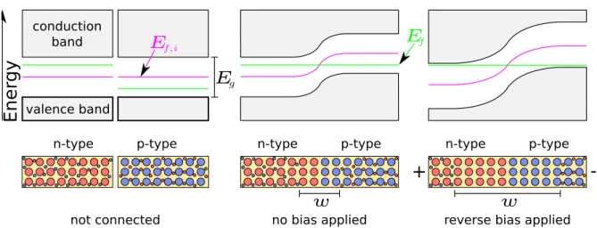
Figure 2.1: Working principle of the pn-junction. The upper images show the energy band structure in the n- and p-type silicon. The lower images visualize the acceptors, donors, electrons, and holes (large blue, large red, small blue, and small red circles, respectively) in the doped silicon materials. The width of the depletion zone is denoted by w.
2.1 Working principles of silicon pixel sensors
While for single atoms electrons are confined to discrete energy levels, in condensed matter the electron wave functions of many atoms overlap, leading to continuous but possibly separated energy bands of phase-space states. The uppermost completely filled band is referred to as valence band while the lowest partially or not occupied band is called conduction band (see left side of Fig. 2.1). The probability f e that a phase- space state of energy E is occupied by an electron can be described by the Fermi-Dirac statistics [58]:
f e (E) = 1
e (E−E
f)/kT + 1 . (2.1)
Here k is the Boltzmann constant and E f is the Fermi energy at which f e (E f ) = 1
2 . (2.2)
The temperature T determines the width in energy of the transition region between
f e (E) ≈ 0 and f e (E) ≈ 1. Depending on the band gap E g between the valence and
conduction band and the position of E f , condensed matter can be classified into insula-
tors, conductors, and semiconductors. The latter are defined as having a band gap of
0 eV < E g . 3 eV which contains E f . Hence, at T → 0 K all phase-space states in the
valence band are occupied, whereas the conduction band is empty. Since no electron
2.1. Working principles of silicon pixel sensors 23 in the valence band can change to a state with a different momentum, a current is not possible.
The energy supplied by ionizing particles can lift electrons from the valence band into the conduction band, where they can move through the crystal. In a semiconductor sensor, these free charge carriers are propagated towards attached readout electronics in an electric field, created by applying different potentials at opposing sensor surfaces.
This induces a time dependent current I e (t) in the electronics that forms part of the measured signal. At the same time the empty phase-space state in the valence band can be occupied by a neighboring valence electron. Hence, the empty space, usually interpreted as a positively charged particle called hole, is - compared to the electrons - propagating in the opposite direction and generates an additional hole current I h (t) 1 .
Silicon is the most prominent example of all semiconductor detector materials and it is used for the sensors relevant for the presented work. On average for each 3.6 eV energy lost or 12.5 nm travelled in silicon a minimum ionizing particle (MIP) lifts an electron from the valence band into the conduction band, i.e. creates an electron-hole pair. This leads to an average collectable charge corresponding to 8000 electrons (8 ke) per 100 µm of sensor thickness.
However, intrinsic silicon is not suitable as a sensor material, since at usual working temperatures many electrons occupy phase-space states in the conduction band and would cause a large current in the electric field. This leakage current would be far larger than the current induced by the electron-hole pairs created by penetrating MIPs. To reduce the leakage current and to create a sensor volume with very few free charge carriers, the rectifying properties of a junction between two extrinsic silicon materials is exploited.
2.1.1 The pn-junction
To create sensors with very low leakage currents and a low free carrier concentration, a combination of n-type and p-type silicon is used (Fig. 2.1). In the lattice of these materials, silicon atoms are replaced with dopant atoms having different electron con- figurations. For n-type silicon atoms with 5 valence electrons (e.g. phosphorus) are used to introduce almost free electrons while for p-type silicon atoms with 3 valence electrons (e.g. boron) are implanted to enrich the material with loosely bound holes.
These additional electrons and holes become the majority charge carriers of the respec- tive extrinsic silicon material. In both cases the Fermi energy E f is changed from the intrinsic value E f,i and moves closer towards the valence band or the conduction band for n- and p-type silicon, respectively. Joining these two silicon types the majority charge carriers recombine at the pn-junction between them until the Fermi energy is
1
![Figure 1.2: The new LINAC4 injector and the present PSB-PS accelerator system [33].](https://thumb-eu.123doks.com/thumbv2/1library_info/4015385.1541373/17.892.199.725.180.549/figure-new-linac-injector-present-psb-ps-accelerator.webp)
![Figure 1.5: The present strawman layout [48] of the inner detector for the ATLAS detector at the sLHC.](https://thumb-eu.123doks.com/thumbv2/1library_info/4015385.1541373/23.892.169.713.192.522/figure-present-strawman-layout-inner-detector-atlas-detector.webp)
![Figure 2.5: Monte Carlo simulation of the interaction of a PKA with an initial energy of 50 keV in silicon [75]](https://thumb-eu.123doks.com/thumbv2/1library_info/4015385.1541373/40.892.273.614.201.570/figure-monte-carlo-simulation-interaction-initial-energy-silicon.webp)
![Figure 2.8: Measured change of the effective doping concentration as a function of the time during controlled annealing at 60 ◦ C with fitted contributions of short term beneficial annealing, long term reverse annealing, and stable damage [92].](https://thumb-eu.123doks.com/thumbv2/1library_info/4015385.1541373/46.892.219.674.198.502/measured-effective-concentration-controlled-annealing-contributions-beneficial-annealing.webp)