Technical University of Munich
Max Planck Institute for Physics
Graduation paper from the Master of Science in Physics
Investigation of the Detector Response to Electrons of the TRISTAN
Prototype Detectors
Untersuchung der Detektorantwort auf Elektronen der TRISTAN Prototyp Detektoren
Daniel Benedikt Siegmann 03640314
15 April 2019
Faculty for Physics
Primary reviewer: Prof. Dr. S. Mertens Supervisors: Tim Brunst
Secondary reviewer: Prof. Dr. S. Sch¨onert
Abstract
Sterile neutrinos are a minimal extension to the standard model of particle physics and can tackle a large number of open questions. One of them is the composition of dark mat- ter in the universe, which could be explained by sterile neutrinos in the kilo-electron-volt mass range. Laboratory experiments that measure β-decay spectra to a high precision can be sensitive to these particles, since their mass eigenstate would manifest itself as a kink-like structure in the spectrum. To measure this imprint of sterile neutrinos the TRISTAN project aims to extend the KATRIN setup with a sophisticated multi-pixel detector system, which can handle high rates with an excellent energy resolution.
In the scope of this thesis, the first TRISTAN silicon drift detector prototypes were charac- terized with electrons. For this purpose a scanning electron microscope that can produce electrons between 0.5 keV and 30 keV has been used. Since the entrance window thickness of the silicon drift detectors influences the shape of the detector response, this detector property had to be minimized in the detector fabrication process and measured precisely.
To achieve this goal, two measurement techniques were developed and compared to es- timate the thickness of the entrance window. The first method uses the overall energy shift between the deposited energy in the sensitive detector volume and the true incoming energy to determine the entrance window thickness. For the second method the detec- tor has been tiled, which artificially increases effective entrance window thickness. This change of the effective entrance window is measured by an energy shift of the spectrum and is then correlated to the entrance window thickness. For both methods the entrance window is modeled as a completely dead layer. In the results presented in this thesis both methods are in good agreement with each other.
For the standard detector technology a dead-layer thickness of (52±7) nm were measured.
Additionally, two detectors with different entrance window technologies were investigated.
Nevertheless, no major advantage of these detectors for the TRISTAN project were found.
The first steps to model the response of the detector with Monte Carlo simulations of electrons in silicon were performed. In addition to this an empirical model was developed to describe the response with analytic functions.
Contents
1 Introduction to Neutrino Physics 1
1.1 Active Neutrino Physics . . . 1
1.1.1 Brief Summary of the Discovery of Neutrinos . . . 1
1.1.2 Neutrinos in the Standard Model . . . 2
1.1.3 Neutrino Oscillations . . . 3
1.1.4 Direct Neutrino Mass experiments . . . 4
1.2 Sterile Neutrino Physics . . . 6
1.2.1 Motivation from Particle Physics . . . 6
1.2.2 Motivation from Cosmology . . . 8
2 keV-Sterile Neutrino Search in a KATRIN-like Experiment 11 2.1 KATRIN Experiment . . . 11
2.1.1 Windowless Gaseous Tritium Source . . . 11
2.1.2 Transport and Pumping Section . . . 13
2.1.3 Spectrometers . . . 13
2.1.4 Focal Plane Detector . . . 14
2.2 Imprint of Sterile Neutrinos in β-Decay Spectra . . . 16
2.3 Requirements to a Novel Detector System . . . 19
3 Silicon Drift Detectors 23 3.1 Basic Principle of Semiconductor Detectors . . . 23
3.2 Working Principle of Silicon Drift Detectors . . . 25
3.3 Entrance Window and Partial Event Model . . . 30
4 TRISTAN Prototype Detector Setup 33 4.1 Detector System with the TRISTAN Prototype SDDs . . . 33
4.1.1 TRISTAN Prototype Detectors . . . 33
4.1.2 Readout-Chain . . . 37
4.2 Scanning Electron Microscope as Source for Mono-Energetic Electrons . . . 40
4.3 Optimization of the DAQ-Settings . . . 44
4.4 Reference Calibration with Photons from an 241Am-Source . . . 46
5 Investigation of Entrance Window Effects with Bremsstrahlung 49 5.1 Calibration of the SEM with Bremsstrahlung . . . 49
5.2 Determination of the Energy Shift . . . 52
5.3 Determination of Dead-Layer Thickness . . . 53
5.4 Conclusion . . . 54
6 Investigation of Entrance Window Effects with the Tilted Detector Method 57 6.1 Measurement of Energy Shift for the Tilted Detector Method with Mono- Energetic Electrons . . . 57
6.2 Determination of Dead-Layer Thickness . . . 59
6.3 Conclusion . . . 61
6.4 Comparison of Standard Technology Detectors . . . 61
6.5 Comparison of Entrance Window Doping Profiles . . . 63
7 First Steps Towards a Full Model of the Detector Response 67 7.1 Full Monte Carlo Simulation to Model the Detector Response . . . 67
7.2 Modeling an Analytic Detector Response . . . 70
8 Conclusion 75 A Appendix 77 A.1 Calculation for Fano-Limit of Silicon . . . 77
A.2 Error Calculation for Calibration . . . 79
A.3 Error Calculation for Energy Shift Measurements . . . 80
A.4 Current Status of the TRISTAN Project . . . 81
1 Introduction to Neutrino Physics
The properties of neutrinos are one of the main questions of modern particle physics.
They take a unique role in the Standard Model, since they only interact via the weak interaction and investigations of their mass and the possibility of them being Majorana particle are topic of current experiments.
To give insight to neutrino physics a brief introduction is given in this chapter, starting with the weakly interacting neutrinos, also called left-handed or active neutrinos. Thereby, the theory of the massless neutrino in the standard model and its extension to neutrinos with a mass, predicted by neutrino oscillations, is discussed. Section 1.1.4 briefly reviews some experimental methods to determine neutrino mass.
The second part of this chapter focuses on the theory of sterile neutrinos which can be right-handed. In detail the motivation, coming from particle physics and cosmological observations, for these particles is discussed in section 1.2.1 and 1.2.2. The main focus is set on keV-sterile neutrinos and current constrains by cosmology.
1.1 Active Neutrino Physics
At the beginning of this section, a brief summary of the discovery of the neutrino will be given, which leads to the role of neutrinos in the Standard Model. First, neutrinos are assumed to be massless, even though neutrino oscillations demonstrate that neutrinos have a non-zero mass as described in section 1.1.3. Experiments to measure the neutrino mass are described in section 1.1.4.
1.1.1 Brief Summary of the Discovery of Neutrinos
In 1930, the neutrino was first postulated by Wolfgang Pauli to explain the continuous spectrum observed inβ-decays. The observed spectrum contradicted the well understood mono-energetic lines seen inα- and γ-decays. The predicted particle had to be orders of magnitudes lighter than the nucleus and the electron, while it also had to be electrically
1 Introduction to Neutrino Physics neutral to explain the decay.[1]
Frederick Reines and Clyde Cowan detected the (electron anti-) neutrino via the inverse β-decay process in 1955.
νe+p−→e++n (1.1)
To obtain an intense anti-neutrino flux, they built their detector next to the Savannah River reactor. The detector consisted of a water tank and scintillators to detect the γ- rays created by the annihilation of the positron. An additional signal of photons with an energy of 2.2 MeV is created by capturing the neutron on cadmium in water. This process occures with a time delay of 200 ns. With this coincident signal the inverseβ-decay could be detected and the observed cross section agreed with the prediction by weak interaction theory [2].
In addition to the detection of the electron anti-neutrino, the team led by Leon Led- ermann, Melvin Schwartz and Jack Steinberg could show that more than one flavor of neutrinos exists. In 1962, they used the decay of charged pions to produce muons and their associated neutrino νµ. The third type of neutrino was discovered at the Stanford Linear Accelerator Center in 1975 and was identified as the tau neutrino ντ.
Studies on the decay of the Z-boson could determine the total number of light neutrinos.
The total decay width ΓZ of the Z0-resonance includes the hadronic decay width Γhad (Z0 →qq), the common partial leptonic width Γl (Z0 →ll) for the charged leptons and the invisible width Γinv =Nν ·Γµ for the neutrinos. From a combination of experiments at the Large Electron-Positron Collider at CERN, the number of light neutrinos has been obtained asNν = 2.9841±0.0083 [3], which is in excellent agreement with the theoretical expectation of three light active neutrinos[2].
1.1.2 Neutrinos in the Standard Model
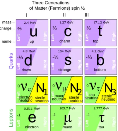
The Standard Model of particle physics includes six quarks of different flavors and three charged leptons, which all exist with left- and right-handed chirality. In addition to these fermions three neutral leptons, the neutrinos, are included with the same flavors as their charged leptonic partners. The model for all fermions can be seen in figure 1.1. In the further discussion only particles will be treated, even though the arguments can easily be transferred to their anti-partner.
Neutrinos are unique in the standard model in such a way that they solely interact through the weak interaction.[4] Since the weak interaction only couples to left-handed particles and neutrinos are electrically neutral, a right-handed neutrino would not interact at all.
1.1 Active Neutrino Physics
Figure 1.1: Standard model of elementary particle physics for fermions
In purple the six quarks are shown with left- and right-handed chirality, while all known leptons are marked in green. The charged leptons are represented in both chirality states like the quark, in contradiction to neutrinos, which are introduced in the Standard Model as massless and only left-handed. (Scheme adapted from [5])
Therefore, neutrinos can only exist as left-handed particles in this model.
1.1.3 Neutrino Oscillations
In the 1960s, the first neutrino detectors that could measure neutrinos from the sun were built. The measurements performed by experiments like the Homestake experiment [6]
by Ray Davis observed a deficite of a factor of three of the neutrino flux from the sun with respect to the predictions. This lead to the so-called solar neutrino problem in the late 1960s. These oberservations were confirmed by various experiments with different detector technologies like the experiments GALLEX [7] and Super-Kamiokande [8].
With the SNO Experiment [9] around the turn of the millennium, it was possible to mea- sure all neutrino flavors via the neutral current interactions. The total neutral rate was in agreement with the solar model, only the flavor was not in accordance, what can be explained by the capability of neutrinos to change their flavor on the way between the
1 Introduction to Neutrino Physics sun and the earth.
This phenomenom is called neutrino oscillation and is further confirmed by the obser- vations of reactor, accelerator and atmospheric neutrinos [10]. The oscillation is raised by the mixing between the flavor and the mass eigenstates of neutrinos. Neutrinos are produced and interact in their flavor eigenstates (νe, νµ, ντ) of the weak interaction, but they propagate in their mass eigenstates (ν1, ν2, ν3). To connect the two different types of eigenstates thePontecorvo–Maki–Nakagawa–Sakata (PMNS) matrix can be introduced.
νe νµ ντ
| {z }
flavor eigenstates
=
Ue1 Ue2 Ue3 Uµ1 Uµ2 Uµ3 Uτ1 Uτ2 Uτ3
| {z }
PMNS matrix
·
ν1 ν2 ν3
| {z }
mass eigenstates
(1.2)
The PMNS matrix for three neutrinos can be parameterized to three mixing angles (θ12,θ13,θ23) and a phase δCP. In the following the probability to oscillate from flavor eigenstate α to the then measured eigenstate β is given by (1.3). For simplicity reasons only the two-flavor case is shown, but it can be further extended to more flavors.
Pα→β = sin2(2θ)·sin2
1.27·∆m2[ eV2]·L[ km]
Eν[GeV]
(1.3) Ldenotes the traveled distance and Eν gives the energy of the neutrino, while the mixing angle between the mass eigenstates is given by θ. ∆m2 = m22 −m21 is assigned to the difference of the squared masses of the mass eigenstates. If neutrinos were massless
∆m= 0, no oscillation would be possible. Hence neutrinos have to have mass.
1.1.4 Direct Neutrino Mass experiments
With the discovery of neutrino oscillations, it is clear that neutrinos have to be massive.
Nevertheless, oscillations reveal only the mass differences ∆mij and the mixing anglesθij but are not capable of measuring the absolute mass of the neutrino mass eigenstates.
From cosmological models, limits to the neutrino masses can be set. Nevertheless since they depend on more parameters than the neutrino masses itself, the focus of this thesis will be on the direct measurement techniques in laboratory based experiments.
Single β-decay
One approach to measure the effective mass of the electron anti-neutrino are single β- decay experiments. Here the energy of β-decay electrons from e.g. tritium are measured
1.1 Active Neutrino Physics precisely close to their kinematic endpoint, as it depends on the neutrino mass and is shifted to lower energies compared to the massless case. The current resolution of the measurement of the endpoint of the spectrum is not precise enough to resolve all three mass eigenstates. Therefore, the effective electron anti-neutrino mass is introduced.
mνe = s
X
i
m2i|Uei|2 ≤2.05 eV (1.4)
Examples for experiments that measured the (single) β-decay precisely are the Mainz [11] and Troisk Experiment [12] that set the current best limit for the effective elec- tron anti-neutrino mass of 2 eV (95%C.L.) [12] [11]. TheKArlsruherTRItiumNeutrino (KATRIN) experiment [13] is expected to surpass this limit in the next years to reach a sensitivity of
mνe ≤0.2eV (90% C.L.) (1.5)
Neutrinoless double β-decay (0νββ)
Another method to measure the neutrino mass is the neutrinoless doubleβ-decay (0νββ).
This process is forbidden in the Standard Model due to the violation of the total lepton number and is only feasible, if the neutrinos are Majorana particles and therefore their own anti-particles.
For this second-order weak interaction process the nuclei has to have an even proton numberZ and even neutron numberN where the singeβ-decay is energetically forbidden.
The discovery of the hypothetical 0νββ-decay would be a direct detection of physics beyond the Standard Model and prove that neutrinos are Majorana particles. In addition to this, the effective Majorana massmee of the neutrino could be observed by the half-life of the decay [15].
mee =
P3
i=1Uei2mi
(1.6)
1 Introduction to Neutrino Physics
Figure 1.2: Feynman diagrams for double β-decays
On the left-hand side the Feynmann diagram for the double β-decay (2νββ) is shown. The right-hand side demonstrates the neutrinoless doubleβ-decay (0νββ). In this case the neutrino has to be its own anti-particle and is therefore a Majorana particle.(Scheme adapted from [14])
1.2 Sterile Neutrino Physics
As shown in section 1.1.2 neutrinos take a unique role in the Standard Model, as they are introduced only with left-handed chirality, while all the other leptons can have both. A natural extension to this model are right-handed neutrinos. Since neutrinos only interact with the weak force a right-handed neutrino would not interact at all, except of the mixing to (left-handed) active neutrinos. Therefore this kind of neutrinos is also called sterile neutrino.
This expansion of the Standard Model is shown in figure 1.3 where now all fermions would have left- and right-handed partners, which would mace the families of fermions more uniform between each other. In addition to this ’natural’ extension, sterile neutrinos could explain the lightness of the active neutrinos and are also dark matter candidates.
In the following sections, these topics are briefly discussed. The main focus will be set on hypothetical keV-sterile neutrino, which the TRISTAN project aims to look for.
1.2.1 Motivation from Particle Physics
One motivation for right-handed neutrinos is that their existence can introduce mass for neutrinos. This is accomplished by adding a mass-term to the Standard Model La- grangian. The combination of the left- and right-handed neutrino with the Higgs field leads to a Dirac mass-term for neutrinos to give them mass, similar as for the other fermions in the Standard Model. Taking into account the current limits for the neutrino
1.2 Sterile Neutrino Physics
Figure 1.3: Standard model of elementary particle physics for fermions in addition of three sterile neutrinos
In purple the six quarks are shown with left- and right-handed chirality, while all known leptons are marked in green and are also represented in both chiral states. In addition to the known neutrinos three right-handed neutrinos are in yellow. (Scheme adapted from [5])
1 Introduction to Neutrino Physics
mass of 2 eV this requires a Yukawa coupling in the order of 10−12, which is five orders of magnitude smaller than the coupling for electrons.
Another way to introduce mass for neutrinos is described by the See-Saw mechanism. For this model, the neutrino is assumed to be a Majorana particle, with the possibility of a transition from a neutrino to an anti-neutrino. By allowing this, the neutrino mass matrix for a single generation can be written with the Dirac mass termmD and a Majorana mass term mR as seen in equation 1.7.
M = 0 mD mD mR
!
, λ1 ≈mR, λ2 ≈ −m2D
mR (1.7)
The diagonalization of M leads to the eigenvalues λ1 and λ2. These eigenvalues are proportional to the physical neutrino masses. Introducing a heavy Majorana massmR in the order of GeV or higher could explain the lightness of the active neutrino, as the other mass-eigenvalue λ2 is inverse proportional to mR.
1.2.2 Motivation from Cosmology
Recent observations of the Planck satellite show that the universe is composed of about 68% dark energy, 27% dark matter and 5% baryonic matter. This raises the question about the composition and origin of dark energy and dark matter. The term dark energy describes an unknown form of energy, which is hypothesized to be the reason for the accelerated expansion of the universe and will not be discussed in this thesis. Dark matter on the other hand is defined as a form of matter that is non-luminous and only interacts weakly. For this dark matter the Standard Model does not provide any suitable candidates that are electrically neutral and stable with respect to the age of the universe.
In this thesis, keV-sterile neutrinos will be discussed as dark matter candidates.
The possibility that active neutrinos explain dark matter is firmly ruled out, since they form Hot Dark Matter (HDM) which leads to a washing-out of small scale structures.
This disagrees with observations on the scale of galaxies. Currently the best agreement of observation and simulation is obtained withCold and WarmDark Matter (CDM and WDM)[16].
Sterile neutrinos in the mass range of O(keV) are candidates for both warm and cold dark matter. Both scenarios fit equally well on large scale structures of the size of galaxy clusters and larger. On smaller scales, the observation of dwarf galaxies and the galactic density profiles fit better to the WDM model and solve many of the existing tensions of the CDM model[17].
1.2 Sterile Neutrino Physics
Figure 1.4: Constraints on the sterile neutrino dark matter mass and mixing angle The white area describes the allowed area for the case where the sterile netrino contributes to 100%to dark matter. The grey area is excluded due to an overproduction or underproduction of dark matter in the early universe. In purple the constraints from the observation of the Lyman-α forest and the Tremaine-Gunn bound is shown. The red and green area is excluded due to the non-observation of the decay of sterile neutrinos seen in mono-energetic X-ray lines. The blue data point corresponds to a controversial unidentified3.5 keVemission line in stacked galaxy cluster measurements. (Plot adapted from [19])
Astronomical observations set further constraints on the allowed parameter space of the sterile neutrino mass ms and the mixing angle θs. This can be seen in figure 1.4. The white region describes the allowed keV-sterile neutrino parameter space for the case in which sterile neutrinos form the entire dark matter. Calculations of the formation of the early universe set constraints to this parameter space due to over- or underproduction of dark matter for very large and small mixing angles. In addition to these confinements from the model of the early universe, a robust and model-independent bound is given by the phase space density of fermionic dark matter, which has to be smaller than the density of a degenerated Fermi gas [18]. Therefore, a lower limit ofms >1keV can be set.
The non-observations of mono-energetic X-ray lines originating from the decay of sterile neutrinos to an active neutrino and a photon set further bounds on the allowed parameter space.
The combination of all these constraints lead to a partly model-dependent but stringent allowed parameter space of 1 keV< ms<50 keV and 10−13<sin2(2θs)<10−7. [16]
1 Introduction to Neutrino Physics
2 keV-Sterile Neutrino Search in a KATRIN-like Experiment
Sterile neutrinos could manifest themselves in β-decay spectra as a kink like structure.
In this chapter the KATRIN experiment is introduced, since it has, next to the measure- ment of the effective neutrino mass mνe, the potential to search for sterile neutrinos. To accomplish this task, a detector upgrade after its measurement phase for the neutrino mass is required. The requirements to build such a novel detector system are presented in section 2.3.
2.1 KATRIN Experiment
The KATRIN experiment is a tritium β-decay experiment, using a Magnetic Adiabatic Colliminator and Electrostatic high-pass filter (MAC-E). It is designed to measure the effective electron anti-neutrino mass seen in equation (1.4). The effect of the neutrino mass on the energy spectrum of tritium is a shift of the endpoint energyQ of the electrons as illustrated in figure 2.1.
KATRIN is designed to reach a sensitivity of 200 meV at 90% confidence level (C.L.) for the effective neutrino massmν[13]. In this chapter, the major components of the KATRIN experiment shown in figure 2.2 are shortly introduced. For a more detailed explanation refer to the KATRIN design report [13].
2.1.1 Windowless Gaseous Tritium Source
The Windowless Gaseous Tritium Source (WGTS) provides an ultra stable and highly luminous gaseous tritium source. The tritium gas with a purity of more than 95% is continuously injected into the source and monitored to keep the decay rate stable at 1011 decays per second wit a maximal variation of 0.1% [13]. This leads to a throughput of 40 g of tritium per day. To ensure a high tritium density for the rate and a reasonable pressure to reduce the Doppler broadening, the source is cooled to 30 K with a stability
2 keV-Sterile Neutrino Search in a KATRIN-like Experiment
Figure 2.1: Theoretical differential tritium β-decay spectrum
In blue the tritium spectra with a neutrino mass of mν = 0 eV is shown. A zoom on the endpoint region with various effective neutrino masses mν is shown on the right-hand side.
(Plot adapted from [20])
Figure 2.2: Schematic of KATRIN Experiment
a) rear section, b) Windowless Gaseous Tritium Source (WGTS), c) transportation sec- tion, d1) pre-spectrometer, d2) main spectrometer, f) Focal Plane Detector (FDP) (Scheme adapted from [21])
2.1 KATRIN Experiment of 0.1%.
The gas gets injected in the center of the WGTS and streams freely to both ends. Here, the tritium gets pumped away by multiple turbo-molecular pumps and later is re-injected after passing through a sophisticated process of purification and cleaning performed in the looped system of the Karlsruher Tritium Laboratory (TLK) [22][13].
2.1.2 Transport and Pumping Section
The tritium in the WGTS must not reach the spectrometer, as it would create a mayor source of background. To prevent this, theDifferential andCryogenic PumpingSections (DPS and CPS) reduce the tritium flow continuously by 14 orders of magnitude. The DPS decreases it by five orders of magnitude with four differential turbo-molecular pumps.
The remaining tritium is then trapped in the CPS by cryo-absorption on argon frost with a temperature of 3 K.
Additionally, the transport section is built in a chicane shape to further prevent that neutral molecules enter the spectrometer. Using these techniques, it is possible to guide the electrons from the source to the spectrometer without passing any solid divider where they could lose energy.
2.1.3 Spectrometers
The main spectrometer is a large MAC-E filter. A negative electrical potential in the middle of the spectrometer at an energy qU filters the electrons by their energy like a high-pass filter. Electrons with lower energy will be reflected by the electric field, while electrons with higher energy will overcome the potential and make their way to the detector. Because the electrons are guided along magnetic field lines, they perform a cyclotron motion as shown in figure 2.3. There momentum is therefore not parallel to the electric field lines and electrons can be rejected even though they would have enough energy. To minimize this effect, a gradient in the magnetic field is created by setting the magnetic field of the source BS and the detector BD to several magnitudes higher values than the magnetic field Bmin in the middle of the spectrometer. This performs an adiabatic transformation of the orthogonal part of the electron’s momentum p⊥ to the parallel momentumpk. This behavior can be seen at the bottom of figure 2.3. The energy resolution ∆E of the MAC-E filter is given by
∆E
E = BMin BMax
(2.1)
2 keV-Sterile Neutrino Search in a KATRIN-like Experiment
Figure 2.3: Working principle of a MAC-E filter
The black lines illustrate the magnetic field lines between the two pinch magnets in blue. The electric field is represented by the green arrows with the maximal potential in the middle of the Spectrometer. In orange the cyclotron motion of an exemplary electron allong the magnetic field lines is shown. The change of the momentum for the electrons through the spectrometer can be seen at the bottom. (Scheme adapted from [22])
Since the magnetic flux Φ = B·A is constant, the spectrometer must be larger than the source. The dimensions of the main spectrometer of 23.28 m length and a diameter of 9.8 m in the cylindrical section allow an excellent energy resolution of about 1 eV [13] for magnetic fields of Bmax = 6T and Bmin = 3·10−4T.
The common operation mode for KATRIN is an integral measurement, meaning that the count rate for different retarding potentials qU of the MAC-E filter is measured.
2.1.4 Focal Plane Detector
The FocalPlaneDetector (FPD) is positioned downstream the main spectrometer. It is segmented into 148 pixels to account for the radial dependence of the incoming electrons.
The detector consists of an monolithic silicon p-i-n diode, whose working principle is explained in chapter 3.1. The detector is grouped into 12 concentric rings of each 12
2.1 KATRIN Experiment
Figure 2.4: Pixel layout of Focal Plane Detector (FPD)
The detector is segmented into 12 rings with each 12 segments and the bullseye in the middle with four segments. Resulting in 148 segments of same size. (Layout adapted from [21])
Table 2.1: Table of measured and calculated properties for the FPD[23]
Detector Property 1 Value
Waver thickness 503µm
Dead layer thickness (’insert-slap’) (155±0.5stat±2.2sys) nm Detection efficiency (95±1.8stat±2.2sys)%
Energy resolution (FWHM) at 18.6 keV (1.52±0.01) keV
Detector capacity 8.2 pF (design value)
Energy threshold at shaping time 0.8µs ≈8.5 keV Energy threshold at shaping time 6.4µs ≈4.0 keV
segments and a bulls-eye of four pixels in the middle. The diameter of the detector is 90 mm and each pixel has a size of 44 mm2. Further properties of the detector can be seen in table 2.1.
Since the energy resolution is given by the MAC-E filter and the region of interest is the energetic endpoint of the tritium spectrum, the FPD is designed to reliable detect electrons at low rates. The current read-out speed allows a maximal rate of 62 kcps for the entire detector (i.e. ≈420 cps per pixel) [23].
In the operated integral mode of KATRIN this read-out speed is adequate. However, for possible future measurements of sterile neutrinos in the decay spectra of tritium it is of significant importance to handle much higher rates to scan deeper into the spectrum.
This topic is discussed in the next section.
2 keV-Sterile Neutrino Search in a KATRIN-like Experiment
2.2 Imprint of Sterile Neutrinos in β-Decay Spectra
As described in sections 1.1.4 and 2.1, the mass eigenstates ν1, ν2 and ν3 of the neutrino show an (effective) imprint of themselves near the endpointQof the spectrum. A similar imprint could be seen for the addition of a fourth mass eigenstate ν4 resulting in an additional sterile neutrino flavor νs. The effect on the spectra is described in equation 2.2 and can be seen largely amplified in figure 2.5.
dΓ
dE = cos2 dΓ
dE
mνe
Θ(E0−E−mνe)
| {z }
Active neutrino part
+ sin2 dΓ
dE
ms
Θ(E0−E−ms)
| {z }
Sterile neutrino part
(2.2)
The kinetic energy of the emitted electron is described as E and the endpoint of the spectrum as E0. The mixing angle between sterile and active neutrino is denoted as θ.
The superposition of the effective neutrino spectra and the sterile spectra would lead to a kink at an energy of E0−ms.
One of the main advantages of the KATRIN experiment is the strength of the high- luminous tritium source in the WGTS. The endpoint energy of E0 = 18.6 keV would theoretically allow the investigation of sterile neutrino masses up to this value. Sensitivity studies that fit the entire tritium spectrum, including a keV-sterile neutrino, show a possible statistical sensitivity with the KATRIN framework to mixing angles of sin2(θ) = 10−6 to 10−8[24] which can be seen as well in figure 2.6. The study is performed for two working modes of KATRIN, the integral measurement as described before, with the variation of the retarding potential qU, only scanning to lower energies where the energy resolution is given by the MAC-E filter and the detector only counts the arriving electrons.
For the differential mode the MAC-E filter is turned off or set to a fixed retarding potential qU. Therefore the resolution is completely given by the detector. The sensitivity study [24] shows that the imprint of the kink-like structure is stronger for the differential mode.
Using the current source strength of KATRIN of N = 8.3·1018 decays in three years the limits set by cosmology can be cross-checked and even further improved.
2.2 Imprint of Sterile Neutrinos in β-Decay Spectra
Figure 2.5: Signature of sterile neutrino in differential tritium spectrum
The theoretical differential tritiumβ-decay spectrum without any sterile neutrino is represented in black. In blue a total spectrum with a sterile neutrino of mass ms = 10 keV and an unreasonably high mixing angel of sin2(θ) = 0.2 is shown. The dotted blue lines mark the sterile part and the active part of the spectrum. (Plot adapted from [20])
2 keV-Sterile Neutrino Search in a KATRIN-like Experiment
Figure 2.6: Statistical sensitivity plot for sterile neutrino parameters
The statistical exclusion plot limits for both differential and integral measurement at 90%C.L.
within three years of measurement for a generic detector efficiency of 90% are shown in this plot. The solid red and blue lines correspond to the sensitivity using the designed source strength (total decays N = 8.3·1018 in three years) of KATRIN for a differential and integral measurement. In gray the exclusions from cosmology are shown. (Plot adapted from [24])
2.3 Requirements to a Novel Detector System
2.3 Requirements to a Novel Detector System
Since the current detector system for KATRIN has been designed for an active neutrino search, it does not fulfill most of the requirements set for the search for sterile neutrinos.
Therefore, theTRitiumInvetigations of STerile toActiveNeutrino mixing (TRISTAN) project has been created to developed a novel detector system that can handle the nec- essary requirements for the sterile neutrino search with KATRIN. Since the demands to the detector system for the differential mode are higher, the requirements for a detector operation in the differential mode is discussed. Nevertheless, such a detector can be used in the integral mode as well. The technology of silicon drift detectors is a promising can- didate to fulfill all requirements for the keV-sterile neutrino search. Therefore they will be discussed with this detector type in mind.
To reach a statistical sensitivity to the mixing angle sin2(Θ) and sterile mass ms of in- terest as shown in figure 2.6 a strong source is required. The designed source strength of KATRIN results in approximately one electron per second at the detector, for an re- tarding potential qU set to one electron volt above the endpoint Q. For the TRISTAN Project this will rise to more than 1010 electrons per second at the designed KATRIN source strength. To handle such high rates it is required to distribute the overall rate among many pixel. In addition to this it is necessary for the readout system to perform at small shaping timesτ to reduce the effect of pile-up and increase the rate that can be handled.
The second major requirement of the TRISTAN project is the precise understanding of the entire spectra, to probe the parameter space for mixing angles sin2(θs) of cosmological interest. To accomplish this, the entire spectrum has to be understood to the parts-per- million (ppm) level, which can only be achieved with an excellent energy resolution and a precise understanding of the detector response. If the energy resolution is too bad, this feature will be washed-out. The sensitivity studies described in chapter 2.2 suggest an energy resolution better than 300 eV at 20 keV to detect the kink-like feature.
As one can see in equation (2.3) these two requirements are liked together, since the serial or voltage noise Qseries, and therefore the energy resolution, is anti proportional to the shaping timeτ [25].
Qseries=p
4kT Rs+e2na· Cd
√τ (2.3)
Therefore all other parameters that influence this correlation have to be as small as possible. One crucial parameter is the capacityCdof the detector, which can be very small
2 keV-Sterile Neutrino Search in a KATRIN-like Experiment
Figure 2.7: Visualization of dead-layer effects on the energy spectrum
The simulation of the energy spectrum for mono-energetic electrons with 14 keV interacting with a silicon detector are represented. For the simulation an Noise with a FWHM of 220 eV is assumed and electrons can back scatter and leave the detector as well. In blue the energy spectrum without any effects by the entrance window is shown. In green and red the same simulation with effects by an dead-layer is shown. The simulation is performed with the simulation software KESS [26].
for silicon drift detectors down to Cd = 110fF. In addition to this the noise ena coming from the amplifier has to be small. Cooling to lower TemperaturesT can further decrease the overall noise in the system and allows for shorter shaping times. The Boltzmann constant is denoted ask and Rs describes the series resistance of the detector.
Since electrons continuously deposit energy when they travel through matter effects close to the surface can worsen the overall energy resolution. For silicon drift detectors a lower or non-sensitive volume is always present at their surface, that does not collect all the deposit energy. This effect results in a lower charge collection efficiency at the entrance window side or in the case of a completely non-sensitive area, in a dead-layer.
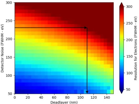
A simulation of mono-energetic electrons at 14 keV under the assumption of the dead- layer model is shown in figure 2.7. One can see that the overall shape of the spectrum changes with increasing thickness of the entrance window and the entire spectrum is also shifted to lower energies. The distortion of the detector response by the entrance window effects as well the resolution as one can see in figure 2.8. A simulation of the Full Width Half Maximum (FWHM) of a mono-energetic electron peak at 20 keV is
2.3 Requirements to a Novel Detector System
Figure 2.8:Energy Resolution for electrons over the noise and dead-layer thickness The visualization shows the energy resolution in therms FWHM for mono-energetic electrons at20 keV for different noise width and dead-layer thickness. Values for the energy resolution for electrons that exciede the300 eV level are shown in dark red. This sets maximum thickness for the dead-layer of110 nm. The simulation is performed with the simulation software KESS [26].
shown over the given noise in the system and the thickness of an dead-layer. Given the defined limit for the energy resolution of 300 eV at 20 keV all values that excited this limit are shown in dark red and can show the allowd properties for the detector system.
Characterization measurements of the TRISTAN prototype detector show that an energy resolution for photons is possible down to 142±3 eV at 6 keV[27]. With a rough estimation of the electronic noise and the Fano limit as shown in section A.1, one can estimate the resolution for the noise and Fano of 235 eV. Using this estimation for the detector noise width in figure 2.8 one can set an upper allowed limit for the thickness of the dead-layer of about 110 nm.
The effects of the entrance window depend on the energy of the incoming electron and are larger for low-energy electrons, since their mean free path is smaller and they interact more often close to the surface. Therefore they deposit most of their energy close to the surface of the detector. For electrons between 1 keV to 6 keV the total deposit energy over the depth is shown in figure 2.9. As an example an electron of 1 keV will in average
2 keV-Sterile Neutrino Search in a KATRIN-like Experiment
Figure 2.9: Average stopping distance of electrons in silicon
The total ratio of deposited energy inside the detector as a function of the depth in the detector is shown. The lines represent the energies between 1 keV to 6 keV and are calculated using simulations with KESS[26] for mono-energetic electrons.
deposit all its energy in the first 40 nm. If this area would be a dead-layer the electron could not be detected and would lead to a detection threshold given by the thickness of the entrance window. This detection threshold limits on one hand the parameter space for the sterile neutrino search, but more importantly it reduces the information of back scattered electrons and charge sharing events in the detector. To guarantee the understanding of the energy spectrum to a ppm-level these low energy events have to measured as well and therefore a very thin entrance window is preferred.
In this thesis the effects created by the entrance window are investigated to understand the detector response of the TRISTAN prototype detectors. To accomplish this task four different silicon drift detectors with ultra thin entrance window technologies are investigated in this thesis. The first goal is to measure the imprint of the entrance window effects in mono-energetic electron spectra and relate it to a physical property of the detector. This will enable the comparison of the different entrance window technologies to select the most promising technology for further investigations as shown in chapter 6.5.
In the next step an empirical model is designed to describe the entire energy spectrum for mono-energetic electrons and its dependency to the angle and energy of the incoming electrons as shown in chapter 7.2.
3 Silicon Drift Detectors
The TRISTAN project aims to fulfill the requirements seen in chapter 2.3 using the promising technology of Silicon Drift Detectors (SDD). These detectors can handle high rates up to 100 kcps with an excellent energy resolution close to the Fano-limit. They are a special kind of semiconductor detectors, that can detect ionizing radiation like photons, electrons and other charged particles as explained in chapter 3.1. The working principle of the SDDs and the underlying technology of sideward depletion is shown in section 3.2.
At the end of this chapter the partial event model for the effects at the entrance window of a SDD is introduced.
3.1 Basic Principle of Semiconductor Detectors
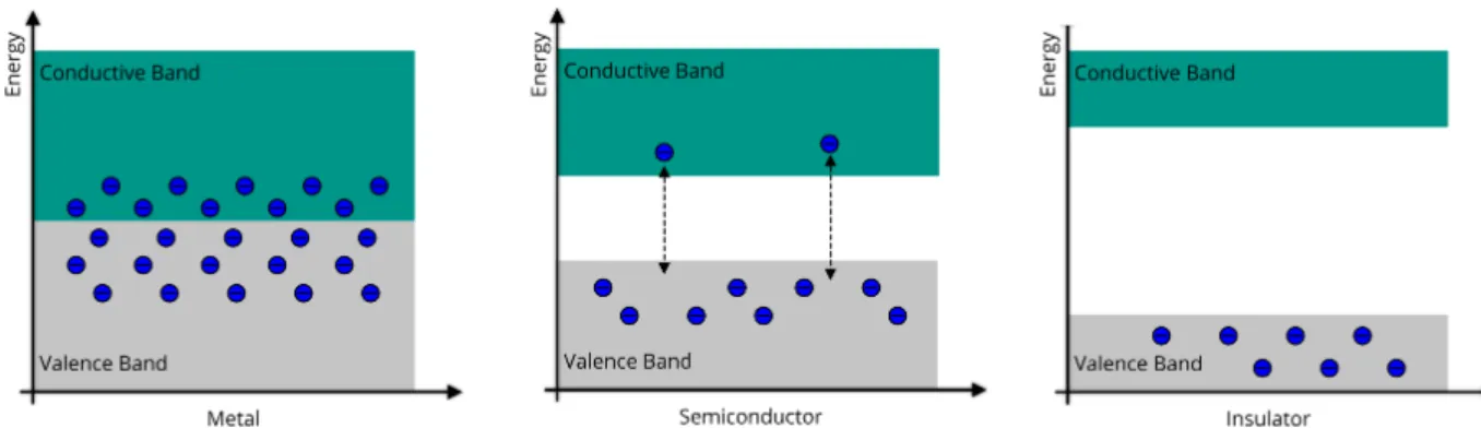
Semiconductor materials, whose conductivity lies between the one of metals and insula- tors. Since the the separation between them is fluid one of the important properties of semiconductors is the fact that their conductivity increases with temperature. Close to absolute zero the valence band is completely occupied while the conductive band is empty.
Therefore no free charge carriers are available to allow conductivity. With increasing tem- perature the probability of electrons in the valence band to get thermally excited to the valence band increases. Therefore more free charge carriers occupies the valence band which increases the conductivity increases. The difference between semiconductors, met- als and insulators in therms of their band structure can be seen in figure 3.1.
A frequently used semiconductor material for detectors is silicon, a type IV material of the periodic table. Next to its availability, the energy to produce a electron-hole pair is rather small with w= 3.6 eV. This allows to create more electrons per deposited energy (e.g. incoming particle), which leads to a overall better resolution compared to other materials.
To alter the conductive behavior, it is also possible to add additional states in the band gap instead of heating the material. This decrease the energy to excite electrons form the valence band to the conductive band and creates free electrons and free holes. This can be achieved by doping the silicon with type V materials e.g. phosphorus to create
3 Silicon Drift Detectors
Figure 3.1: Exemplary band structure for metals, semiconductors and insulators For metals the the valence band and the conductive band are in contact or even overlap.
Electrons can move freely as charge carriers. Insulators on the other hand have a large band gap and all electrons are situated in the valence band which leads to no conductivity. Semi- conductors lie in between these two extreme cases. They are neither good conductors nor insulators, however their conductivity can be increased and controlled by doping.
a n-type semiconductor or by adding material of type III e.g. boron to create a p-type semiconductor. For n-type doping this establishes an energy level close to the conductive band, that produces even at low temperatures free electrons in the conductive band. A similar behavior occurs for p-type doping to create an energy level close to the valence band, with the difference that an additional hole can be created in the valence band.
Free holes increase the conductivity of a material in the same way as free electrons. A visualization of this process can be seen in figure 3.2.
Particles that penetrate material like silicon create electron-hole pairs at every interac- tion point. The number of these created charge carriers are many orders of magnitude smaller than the free charge carriers already existing in an intrinsic silicon substrate at room temperature. The signal can not be distinguished from the thermal charge car- riers, whose number therefore has to be reduced to detect the signal charge carriers in between[28].
This can be achieved by cooling the substrate to very low temperatures close to absolute zero. Nevertheless, the easier solution is to deplete the detector volume, using the princi- ple of a reversed-bias pn-junction to reduce the number of free charge carriers.
A pn-junction is created by connecting an n-doped and a p-doped material of the same concentration with each other. While the n-type material has an overflow of electrons, a p-type has an overflow of holes. These surplus charge carriers move to opposite regions and recombine leaving behind the fixed charged dopant atoms. These oppositely charged atoms create an electric field against the movement of the free charge carriers preventing further diffusion. The resulting ’built-in’ voltage is called diffusion voltage Udiffusion and
3.2 Working Principle of Silicon Drift Detectors
Figure 3.2: Illustration of band structure for doped semiconductors
On the left-hand side the band structure of an n-doped semiconductor is shown. The additional level in the forbidden gap is created by the placed impurity of type V of the periodic table. At room temperature the surplus electron can easily be excited to the conductive band. For the p-doped semiconductor on the right-hand side one electron is missing. This allows an electron to excite to the added acceptor level of the doped atom and leaves a free hole in the valence band. In both cases these free charge carriers increase the conductivity of the semiconductor.
establishes a dynamic equilibrium in the transition area without any free charge carriers, which is called depletion zone.[28]
By applying an additional external voltageUbias in the same direction of the built-in volt- ageUdiffusion, the depletion zone can be increased. The processes involved in the formation of a pn-junction are illustrated in figure 3.3. Incoming particles that interact inside the depletion zone will create a charge cloud of electron-hole pairs. The electrons drift against the electric field to the n-doped side, also called anode, where they can be read out. The holes move to the opposite side and end up at the cathode and can be detected as well.
The collected charge at either side is proportional to the deposited energy of the particle.
This kind of detector is called pin-diode.
3.2 Working Principle of Silicon Drift Detectors
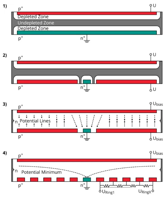
In 1983, the sideward depletion was introduced by E. Gatti and P. Rehak to produce semiconductor detectors for ionizing particles with a low anode capacitance [29]. The resulting detector type is known asSiliconDrift Detector (SDD).
To understand the working principle of SDDs and the sideward depletion, first a normal positiveintrinsic negative (pin)-diode is shown in the top part of figure 3.4. A pin-diode consists of differently doped electrodes on each side of the detector. The entrance side is containing ap+-doped substrate and the bottom side is the anode withn+-doping. With
3 Silicon Drift Detectors
Figure 3.3: Illustration of reverse-bias pn-junction
The creation of a reversed-bias pn-junction is shown in several steps. In the first picture an n-doped semiconductor is shown in blue with additional free electrons and the p-doped semiconductor with additional free holes is shown in red. The corresponding remaining atoms with their charge are represented by the smaller charge symbols while the free charge carriers are described with the larger symbols. In picture 2) the recombination process is illustrated when the two doped materials are connected. The free charged particles recombine with each other and create a depleted zone (illustrated as the grey area) with no free charge particle inside. The diffusion current of the charge carriers and the build-in voltageUdiffusion establishes an equilibrium. The depletion zone can be increased by applying an additional voltage Ubias as shown in the last part.
3.2 Working Principle of Silicon Drift Detectors some voltage U smaller than the depletion voltage Udep, the detector depletes partly as explained for the pn-junctions in chapter 3.1. The sideward depletion is possible since it is not necessary to extend the n+ doped contact over the entire area. It can rather be placed anywhere on the undepleted area. The anode is scaled down and the additional space is filled with p+-doped material. This leads to multiple separated space-charge re- gions as shown in the second part of figure 3.4. By applying a high enough voltageUBias
the depleted zones will touch each other and deplete the entire detector. This double sided diode needs only a fourth of the voltage applied to thep+- electrodes compared to pin-diode of the same size[29].
In this configuration a potential valley for electrons exist, but for regions apart from the anode, the electrons are not guided to the latter. Even though it is possible that these electrons reach the anode via thermal diffusion, the drift times for this will be too slow and it is not possible to associate the electrons to one common event. To solve this problem, an additional electric field is applied parallel to the surface. This is achieved by dividing the bottomp+ bulk into smaller strips and applying a graded potential URingX to URing1
on them. With this additional field electrons are guided to the anode from every point in the detector. A simulation of these fields can be seen in figure 3.5.
The charge collection at the anode is proportional to the measured energy and the drift times of the electrons can be used to calculate the interaction point of the incoming par- ticle. In comparison to the classical pin-diode the anode is much smaller, which decreases the capacitance of the collecting anode to the order of 100 fF[29]. This value is mostly independent of the active area of the detector and therefore allows larger devices with good energy resolution.
The first SDDs were designed with multiple anodes arranged in stripes or matrix like patterns to reconstruct the particle interaction point inside the detector for high energy physics experiments. This could be achieved by measuring the drift times of the created particles to various anodes.
For the TRISTAN project one pixel is created by a radial drift field as shown in figure 3.6. One important benefit of this design, compared to the linear or matrix like devices, is that it is much easier to properly terminate the field lines. The radial symmetric potential valley guides the electrons to the point like anode which is placed in the center.
3 Silicon Drift Detectors
Figure 3.4: Illustration of sidewards depletion
The steps from a pn-junction or pin-detector to a SDD are shown in the parts 1) to 4). The first picture shows a pin-diode where the ohmic contactsn+ for the anode (green) and thep+ electrode (red) extend over the entire surface on both sides of the detector. The principle of sideward depletion shown in the second step. By covering both sides of the detector with p+ electrodes, the n+ anode can be designed much smaller to reach the same level of depletion.
For 1) and 2) the applied bias-voltage U is chosen to be smaller than needed to deplete the entire detector. The depletied region is illustrated in white. The full depletion can be seen in the third part after applying a high enough voltage Ubias. In this way the applied voltage is four times lower compared to a pin-diode of same size[29]. The potential lines for electrons are shown with arrows. To force the electrons to drift towards the anode an additional electric field is applied parallel to the surface. This is achieved by separating the bottom electrode and applying the drift voltages URingX to URing1 as shown in 4).
3.2 Working Principle of Silicon Drift Detectors
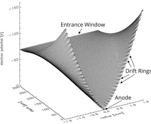
Figure 3.5: Simulation of energy potentials for electrons inside a radial symetric Silicon Drift Detectors (SDD)
The flat area in the back shows the applied voltage at the entrance window side to the p+ electrode. On the radial axis, at a depth of zero, the set potential for the drift rings can be seen. The potential reaches its miniumum at the anode in the middle of the detector. From all points inside the detector electrons are guided to the anode. (Simulation adapted from [30])
Figure 3.6: Schematic diagramm of an SDD for the TRISTAN project
The back contact on the entrance window side as well as the drift rings are doped with p+ material and are shown in red. Then+ anode is shown in green. (Scheme adapted from [30])
3 Silicon Drift Detectors
3.3 Entrance Window and Partial Event Model
When electrons pass trough matter like silicon, they interact almost continuously with it and create secondary electrons and holes. Especially the secondary electrons created close to the surface of the detector behave differently than the secondary electrons in the bulk, as shown in [31] and [32] for incoming photons.
This behavior originates from the electric potential close to the surface of the detector, which can be flat or even guiding the electrons away from the anode, due to the depth of the p+ doping. The simplest model to describe such an effect is a completely non- sensitive layer at the top of the detector, which is called dead-layer. It corresponds to an area where all created secondary electrons are guided to the interface between silicon and silicon oxide, where they recombine with e.g defects and can not be detected any more. This silicon oxide layer is always present, since it builds itself if silicon is in contact with air. By artificially adding a silicon oxide layer it can be created as homogeneously as possible and it also protects the detector from further oxidation. On top of this the silicon oxide layer is required to produce the ultra thin entrance windows as schown in section 4.1.1.
A more sophisticated description of the entrance window effects is given by the partial event model([31], [32]). It takes into account that the charge cloud of secondary electrons can split and only a part of it is lost while the other part gets detected. To encounter this effect the charge collection efficiency of the detector, close to the entrance window, is modified. It is defined as the ratio of collected electrons at the anode compared to the created electrons at a distance z from the entrance window side (z = 0). An analytic formula is developed in [32] and is shown in equation (3.1).
CCE(z) =
0 : z < d S+B z−dl c
: d≤z ≤l+d 1−Ae−z−d−lτ : l+d≤z≤D
(3.1)
with:
A= (1−S) τ c
l+τ c
(3.2) B = (1−S)
1− τ c l+τ c
(3.3) The detector thickness is denoted as D and z describes the depth into the detector, starting at the entrance window side. The parameter S describes the minimal ratio of
3.3 Entrance Window and Partial Event Model
Figure 3.7: Illustration of the charge collection efficiency function
The displayed charge collection efficiency function is motivated from the partial event model.
To draw the collection probability for a SDD the measured values by [33] are used. Silicon oxide thickness d = 10 nm, minimal collection efficiency S = 0.32. Transition parameter l= 50 nm and τ = 50 nm. Curvature parameter c= 1.26.
electrons detected and can take values between 0 and 1. The depth for the influence of the entrance window effects is described by the transition parameterl, which typically lies for SDDs in the range of 50−100 nm and the parameter τ with a typical value of about 100 nm. With the parametercthe curvature in this transition area is adjusted, which can take values between 1 and 2. The thickness of a completely non-sensitive layer on top of the detector (e.g. silicon oxide) is given by d. For the TRISTAN prototypes this oxide layer is aboutd= 8−10 nm thick. A representation of a charge collection efficiency with typical values can be seen in figure 3.7.
3 Silicon Drift Detectors
4 TRISTAN Prototype Detector Setup
In this chapter an overview of the experimental setup is given. The first part describes the detector system with the TRISTAN prototype detectors and the readout system Dante DPP [34]. To generate mono-energetic electrons between 0.3 keV to 30 keV the ScanningElectronMicroscope (SEM) at the HLL is used and is described in section 4.2.
An optimization to reduce the trigger rate on the noise and to minimize the resolution is shown in section 4.3. To compare the measurements of the electron and photons response, each detector is calibrated with photons from an Am241 source. The most intense lines of this source are around 14 keV an 18 keV. Therefore most of the measurements performed with electrons are chosen close to these values as well to be close to the calibration lines with photons.
4.1 Detector System with the TRISTAN Prototype SDDs
To perform first tests with silicon drift detectors for the application in the TRISTAN project, several prototype detectors have been produced. The key features of these pro- totypes are shown in the following section, as well as the setup of the readout electronics.
4.1.1 TRISTAN Prototype Detectors
The investigated SDD chips of the TRISTAN prototype detectors are made of a 450µm thick silicon wafer and consist of seven hexagonal shaped pixels with a diameter of 2 mm.
The hexagonal shape of the pixels enables their arrangement in an array like fashion, without any gaps between the pixels, while still having the benefits of a circular SDD.
The arrangement of the pixels can be seen from the electronics side of detector board in figure 4.1. The nomenclature for them is chosen as the cardinal points and is represented with two letters, defining theCentral pixel as CC and the upper pixel asNNforNorth.
The combination ofNorth andSouth withWest andEast results in the remaining names NW, SW, SS, SE, NE for the pixels.
4 TRISTAN Prototype Detector Setup
Figure 4.1: Picture of the electronic side of the SDD
On the left-hand side a mounted SDD chip is shown with all bonds and installed ASICs seen from the top side. A zoom on an ASIC-Cube [34] and on to the Anode can be seen on the right-hand side. The pictures were taken with an optical microscope.
To fully deplete the detector, the p+-doped area on the entrance window side is set by the back contact voltage to UBackC =UBias =−90 V. To keep all electrons created inside the sensitive area, an additionalp+-guard-ring the detector. It is called back frame and is set to a slightly higher voltage of UBackF =−100 V to prevent that electrons are created close to the edge of the detector from leaving. The two contact points on the back side of the detector can be seen in figure 4.2.
The electric field parallel to the surface is created by twelve drift rings with a gradient between the outer ring at URingX = −110 V and the inner ring at URing1 =−20 V. With this field all electrons created in the sensitive area are guided towards the anode located in the center as seen in figure 4.1. It has a diameter of 90µm leading to a capacitance of 110 fF. The anode is connected with a 18µm thick bond to the first amplification stage, which allows the transport of the signal without further increasing the capacitance. The first amplification is handled by the low noise preamplifier ASIC-CUBE [35]. The position of the ASIC-Cubes around the wafer and the corresponding bonds can be seen in 4.1.
The amplified signal is then routed through the detector-PCB to the output pins. It also handels the routing of the rewired power supplies for the ASIC-Cubes and the detector itself. The detector board can be seen in figure 4.3.
For the investigation of the entrance window different detectors have been produced.
To separate them from each other a naming scheme has been applied to the detectors to identified them. The general naming scheme starts with two letters describing the
4.1 Detector System with the TRISTAN Prototype SDDs
Figure 4.2: Picture of the entrance side of the SDD
On the left-hand side the entrance window side of the detector is seen, while being mounted onto the PCB. The required voltage to deplete the detector and to keep the electrons inside the detector volume is provided via the two bonds for the back contact and the back frame.
A zoom on the bonding connection can be seen on the right-hand side. The pictures were taken with an optical microscope.
Detector board top side Detector board entrance window side Figure 4.3: Detector board overview
The detector board from the top and bottom is shown in this figure. As seen on the bottom side of the detector no SDD wafer is installed.
4 TRISTAN Prototype Detector Setup
Table 4.1: Internal naming scheme for 2 mm prototype detectors
The naming scheme is chosen to directly represent the different entrance window technologies used to produce the detector.
Abbreviation Description
S0 - # Standard radiation
SC - # Standard radiation withCounter implantation R0 - # entrance window with reduced Dose
RC - # entrance window with reduced Dose andCounter implantation entrance window doping profile, as shown in table 4.1, followed by a number.
The doping profile for the standard entrance window has been used in other experiments, too [32], and is highly optimized for the detection of photons. The other versions of the doping profile try to improve this ultra thin entrance window even more. For the entrance window R0 the dose of implants is reduced in the processing which results in an overall reduction of p+-doping and the depth it enters into the material, as shown in figure 4.4. In theory, this should shift the maximum of the electric field closer to the surface, but it comes with the risk that the detector will not be completely depleted if the concentration ofp+-dopendants can not compensate the n-doping. Another way to bring the maximum of the electric field closer to the surface is achieved by counter implanting withn+-dopendants behind thep+-doping. Like the reduced dose technique this entrance window comes with the risk that if the concentrations are not well balanced anymore, the detector does not deplete. The combination of these two techniques whilst producing the RC-detectors, this problem lead to the large inconsistencies up to the malfunction of these detectors. Therefore, in the further work only the working technologies S0, R0 and SC are investigated.
4.1 Detector System with the TRISTAN Prototype SDDs
Visualization of doping profile Visualization of electric field lines Figure 4.4: Vizualization of doping profiles and electric fields
On the left-hand side a visualization of the doping profile for the different entrance window technologies is shown. The standard implantation S0 and the reduced dose R0 are produced with p+-doping. In contrast to this, the SC doping profile is produced with an additional counter implantation ofn+-impurities. An estimation of the electric filed lines is shown on the right-hand side. The plots are based on [36], but do not represent an actual measurement.
4.1.2 Readout-Chain
The bias board filters and provides the routing for all the needed voltage supplies for the CUBE-ASIC and the SDD. In addition to this it sends a common reset signal to all the ASIC-CUBEs on the board. The signal arriving from the detector board gets amplified a second time to drive a coaxial cable to the Data AcquisitionSystem (DAQ). The bias board can be seen in figure 4.5.
An exemplary waveform can be seen between two resets of the ASIC-CUBEs as shown in figure 4.6. The continuous increase of the waveform is created by the leakage current of the detector. A particle interacting with the detector will create many electrons (and holes) in a short time, which charges the input of the ASIC-CUBE and therefore increases the voltage at its output. This signal manifests itself in the waveform as a sharp step. To prevent the ASIC-CUBE from saturation a synchronous reset signal is sent to all ASIC- CUBEs at a set threshold to discharge them. This leads to the steep decrease in the waveform.
To extract the energy information of each event, the waveform is digitized with the DANTE DPP (Digital Pules Processor) and analyzed with two trapezoidal filters. It has a sampling rate of 125 MHz with a 16-bit Analog to Digital Converter (ADC). To trigger on all possible events, which could be above the threshold, a fast trapezoidal filter
4 TRISTAN Prototype Detector Setup
Bias board DANTE DPP
Figure 4.5: Read-out chain hardware
On the left-hand side the bias board is shown. The power supply for the detector and the on board electronics can be connected with a D-Sub 9 connector at the top. Detector and bias board are connected with 25 pin cable on the left. The seven coaxial cables for the signals to the Dante DPP leave on the right. The picture on the right hand side shows the digital pulse processor DANTE DPP by XGLab [34] for eight channels.
is applied to the digitized waveform in the first step. The peaking time and flat top time of this fast filter can be set to values between 8 and 248 ns which allow a fast selection of possible events. This fast filter marks possible events that are above the set threshold.
All events that are preselected by the fast filter are then analyzed with a longer and more accurate energy trapezoidal filter. The energy filter peaking time can be set up to 16µs, while the optimum value for the TRISTAN prototype detectors is around 800 ns with respect to the energy resolution [27]. Events that happen closer together then the time window of the energy filter lead to pileup. Since the fast filter has a much shorter time windows it can detect such events and allows the option to reject these events. For the measurements this feature is used.
The combination of the fast filter and the energy filter allows a precise measurement of the deposited energy in the detector at very high rates and is performed by the Field Programmable Gate Arrays (FPGA) of the Dante DPP. The measured events can then be saved in a histogram or as a list of the time stamp and energy for every occurred event.
A sketch of the setup with the entire readout chain can be seen in figure 4.7.