DEPARTMENT OF PHYSICS
TECHNISCHE UNIVERSITÄT MÜNCHEN
Master’s Thesis
Characterization of the Detector Response to Electrons and Test of a
New Entrance Window Technology of Silicon Drift Detectors for the
TRISTAN Project
Charakterisierung der Detektorantwort auf Elektronen und Test einer Neuen Eintrittsfenstertechnologie für Silizium
Drift Detektoren für das TRISTAN Projekt
Author: Manuel Lebert
Primary reviewer: Prof. Dr. Susanne Mertens Secondary reviewer: Prof. Dr. Stefan Schönert Supervisor: Tim Brunst
Submission Date: 02.12.2019
Abstract
Neutrinos are the most abundant particles with mass in the universe and the lightest ones in the standard model of particle physics. One way to explain the lightness of neutrinos is the introduction of right-handed neutrinos. These would not interact at all and are hence called sterile neutrinos. These theoretical particles would only be a minimal extension of the standard model. If the corresponding additional neutrino mass eigenstate would have a mass in thekeVrange, they could potentially explain dark matter. A special feature of this type of dark matter is that is could be rather warm, which in turn may solve some tensions in the description of small-scale structures in the universe. An imprint ofkeV-sterile neutrinos could be observable in the spectrum of β-decay. The additional heavy mass eigenstate would lead to a very small kink-like structure in the spectrum. The TRISTAN project aims to upgrade the KATRIN experiment with an multi-pixel detector system. The prerequisites of this novel detector system are to: 1) handle high rate, 2) provide an excellent energy resolution, 3) to allow for a precise calibration and modeling of the detector response to electrons. An ideal technology for such applications are silicon drift detector. With this new detector KATRIN could be sensitive to those new particles.
The first objective of this thesis was the characterization of the entrance windows of the first seven-pixel silicon drift detector TRISTAN prototypes with conversion electrons from the metastable 83mKr decay. The second objective of this thesis was the investigation of a novel technique based on molecular beam epitaxy to produce silicon drift detectors with ultra-thin entrance windows.
The entrance window of a silicon drift detector alters the measured energy of incoming electrons and the shape of an electron peak. Therefore, this window has to be as thin as possible. Two detectors with different ion implanted entrance windows were characterized. To this end monoenergetic conversion electrons from
83mKr decay were used. By measuring the position of the electron peaks at different incident angles of the electrons, the entrance window thickness of the detector can be determined largely independent of the energy losses in the source itself.
Finally, the observerd shift of the electron’s peak position can be related to an effective dead layer via Monte-Carlo simulations. The results of energy shift and dead layer are then compared to previous characterizations. The shifts of this work and the previous one’s are compatible.
For the investigations of detectors fabricated with the novel molecular beam epitaxy, at first the leakage current of several hundred pin-diodes was evaluated.
In general, epitaxy pin-diodes have a higher leakage current and therefore a higher failure rate compared to ion implanted ones. In a second step, four representative diodes were chosen and the efficiencies of those were measured with the help of an electron microscope. Of the chosen diodes two were produced using molecular beam epitaxy and two were produced using standard ion implantation techniques.
At incoming electron energies above 10 keV hardly any difference is visible. In the energy range between 1 to 2 keV the efficiencies of epitaxy diodes are above 70 %, while the standard ion implantation technology show only efficiencies of 30 %. Hence, as a major result of this work, it could be shown that the epitaxy technique is superior over implantation for diodes. Based on Monte-Carlo simulations the observed detection efficiencies can again be related to a dead layer. It is found that the entrance window of the pin-diodes produced with the novel epitaxial technique can be described with a thin, approximately 5 nmthick, dead volume. The standard detectors, in contrast, are better described with thick transition layers of up to several hundred nm.
Contents
Abstract iii
1. Introduction 1
1.1. Neutrino Physics . . . . 1
1.2. Sterile Neutrinos . . . . 3
1.2.1. Particle Physics Motivation . . . . 3
1.2.2. Cosmological Motivation . . . . 4
1.3. KATRIN Experiment . . . . 6
1.3.1. Setup . . . . 6
1.3.2. Sterile Neutrino in the β-Spectrum . . . 10
1.4. TRISTAN Project . . . 12
2. TRISTAN Prototype Setup 15 2.1. Functional Principle of the TRISTAN Detector . . . 15
2.1.1. Basic Principle of Semiconductor Detectors . . . 15
2.1.2. Working Principle of an SDD . . . 17
2.1.3. Influence of the Entrance Window on Particles . . . 20
2.2. TRISTAN Prototype Detector . . . 23
2.3. Readout Chain . . . 24
3. Dead Layer Characterization with Conversion Electrons from Krypton 29 3.1. 83mKr Source . . . 29
3.1.1. Decay of83Rb . . . 29
3.1.2. Production of Sources . . . 31
3.2. Description of Experiment . . . 34
3.2.1. Measurement Idea: Tilt-method . . . 34
3.2.2. Experimental Setup . . . 34
3.2.3. Calibration of the Detector . . . 36
3.3. Detector Dead Layer Characterization . . . 38
3.3.1. Analytic Detector Response Function . . . 38
3.3.2. Analysis of Measurements . . . 40
3.3.3. Analysis of Results . . . 44
3.3.4. Conclusion . . . 44
3.4. Dead Layer Thickness Determination . . . 45
3.4.1. Simulation Setup . . . 45
3.4.2. Simulation Results . . . 46
3.4.3. Dead Layer Thickness Conclusion . . . 46
3.5. Source Influence on the Energy Shift . . . 49
3.6. Conclusion . . . 50
4. Epitaxy Entrance Window pin-Diodes 53 4.1. Doping Technologies . . . 53
4.1.1. Ion Implantation . . . 53
4.1.2. Molecular Beam Epitaxy . . . 54
4.2. Prototype Wafers . . . 55
4.3. Leakage Current Investigations . . . 56
4.3.1. Leakage Current Setup . . . 57
4.3.2. Measurement Results . . . 57
4.4. Electron Efficiency Determination . . . 61
4.4.1. Description of Measurement . . . 62
4.4.2. Efficiency Measurement Results . . . 67
4.5. Efficiency Simulation . . . 69
4.6. Summary of Epitaxy Diodes . . . 72
5. Conclusion and Outlook 75
A. Stability of Line Positions 79
B. Uncertainty Calculation 81
C. Epitaxy Wafer Layout 85
D. Epitaxy Results 89
E. Proton Grid 93
List of Figures 97
List of Tables 99
Bibliography 101
Acknowledgments 107
1. Introduction
The neutrino is the most abundant particle in the universe. It was proposed in 1930 by Wolfgang Pauli to explain the continuous β-spectrum. Roughly twenty-five years later it was discovered. They are the only particles in the Standard Model of particle physics, that interact only via the weak force. Therefore, the direct investigation of their properties is extremely difficult. In this chapter a short overview of the currently known properties of the neutrino is given. Afterwards, the hypothetical sterile neutrino is introduced. The cosmological and particle physics observations as motivation for the introduction of a new neutrino are then given. Finally, the KATRIN experiment, measuring the neutrino mass, and its detector upgrade, the TRISTAN, project are described.
1.1. Neutrino Physics
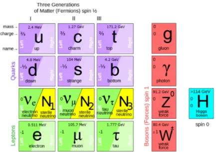
The Neutrino in the Standard Model: The Standard Model (SM) of particle physics describes the fundamental particles and their interaction via the electroweak and strong force, all particles are shown in figure 1.1. The neutrino in this model is a massless particle that comes in three flavors. Neutrinos have no electric charge and therefore, solely interact via the weak force, which couples only to left-handed particles. Thus, a right-handed neutrino would not interact in any way, which makes the neutrino the only particle that exists exclusively with left-handed chirality.
Neutrino Oscillations: Through several experiments it was shown that the neutrino is in fact not massless [6, 18]. This is proven by neutrino oscillation, in which neutrinos change their flavor. The flavor eigenstate of a neutrino(νe, νµ, ντ)is not the same as its mass eigenstate (ν1, ν2, ν3). Each flavor is a superposition of the three mass eigenstates. The mixing between the masses for each flavor is described by the Pontecorvo-Maki-Nakagawa-Sakata (PMNS) matrix (see equation (1.1)).
νe νµ
ντ
| {z }
Flavor Eigenstates
=
Ue1 Ue2 Ue3 Uν1 Uν2 Uν3
Uτ1 Uτ2 Uτ3
| {z }
PMNS Matrix
ν1 ν2
ν3
| {z }
Mass Eigenstates
(1.1)
Figure 1.1.: The particles constituting the Standard Model of particle physics. The neutrinos are the only particles that interact exclusively via the weak force and thus are only left-handed. Taken from [19].
The mass eigenstate is the propagation state of neutrinos, which then leads to the mixing of the flavors. The probability to transition between flavor eigenstate i to another flavor eigenstate j is:
Pi→j ∝sin2
∆m2ijL 4E
(1.2) Here, E is the energy of the neutrino and L is the distance from the creation point.
The mixing probability is only sensitive to the difference of the squared masses of two different mass states ∆m2ij = m2i −m2j. If neutrinos were massless, the mass difference ∆m2ij would be zero and no oscillation would appear. Thus, the existence of neutrino oscillations between all three flavors prove that at least two mass eigenstates are non-zero and the SM is incomplete.
Neutrino Mass: Neutrino oscillations are sensitive to the mass difference of neutrinos. However, they cannot probe the absolute mass scale of neutrinos. For this three methods are currently explored:
The ΛCDM is a cosmological model that describes the evolution of the universe.
Because of their vast abundance, neutrinos have an influence on the structure formation in the universe. They have a long free streaming length and thus wash out small scale structures, which influences the formation of large-scale structures (LSS). Therefore, by analyzing the LSS of the current universe and the anisotropies
1.2. Sterile Neutrinos
of the cosmic microwave background an upper limit on the sum of neutrino masses can be determined. This lies between 0.12 and0.9 eV [4, 15]. However, these limits are extremely model dependent because they differ by which data sample is used and which processes are taken into account during analysis.
The second method is the search for the neutrinoless double β-decay (0νββ):
2n→2p+ 2e- (1.3)
This process is forbidden by lepton number conservation. It is only feasible if neutrinos are Majorana particles, meaning they are their own anti-particles. If this process is observed it would be possible to determine the effective mass of the Majorana neutrinos through the half-life of the decay. The currently best upper limit is 0.2 eV at 90 % C.L. [5].
The third method is by measuring the kinematics of theβ-decay. For this, the spectrum of β-decay electrons is measured. The endpoint is lower, corresponding to the mass of the neutrino, than in a massless neutrino case. This has the advantages of well-known physics and it is hardly model dependent. Currently the resolution of such kinematics measurements is not precise enough to resolve the three different mass states. Therefore, a limit on the effective electron anti-neutrino mass is given:
mνe= s
X
i
m2i |Uei|2 (1.4)
The Karlsruhe Tritium Neutrino (KATRIN) experiment currently set the best upper limit for this effective mass to 1.1 eV at90 % C.L. [7].
1.2. Sterile Neutrinos
As shown in section 1.1 the neutrino of the Standard Model is the only particle that has exclusively left-handed chirality. Therefore, a minimal, natural extension of the SM is the introduction of right-handed neutrinos, as shown in figure 1.2. These neutrinos would not interact at all, except for their mixing with the left-handed neutrinos. Hence, they are called sterile neutrinos.
Depending on the scale of the corresponding new neutrino mass eigenstate (which are mostly made of the right-handed type), sterile neutrinos could explain the small masses of active neutrinos through the seesaw mechanism (O(MeV)) or would be viable dark matter candidates (O(keV)).
1.2.1. Particle Physics Motivation
For the active neutrinos the mass creation mechanism is unknown. Mass creation via interaction with the Higgs field requires changing the chirality, therefore it is
Figure 1.2.: Right-handed neutrinos are a minimal extension of the Standard Model of particle physics. These particles would not interact at all, except for their mixing to the left-handed neutrinos. Thus, they are called sterile neutrinos. Taken from [19].
not possible for only left-handed active neutrinos. By introducing a right-handed neutrino, the Higgs mechanism would be possible for neutrinos. To not exceed the current bounds on the neutrino mass the Yukawa coupling needed for the neutrinos is in the order of 10−12[3]. This is five orders of magnitude smaller then the coupling for an electron.
Another way of introducing small neutrino masses is by the seesaw mechanism.
For this a right-handed, Majorana neutrino with mass mr is introduced. This can be done without the Higgs mechanism. Additionally, a Dirac mass mD is assumed.
Then the mass of one neutrino generation in matrix notation is:
M =
0 mD mD mr
→ m1 =mr, m2 = −m2D
mr (1.5)
This leads to the eigenvalues m1 and m2. Assuming mrmD results in a heavy, right-handed Majorana state and a light active state [3].
1.2.2. Cosmological Motivation
Current observations of the composition of the universe show that only about 5 % consists of baryonic matter, 26 % of dark matter (DM) and 69 % of dark energy [2].
Not much is known about dark energy, but it is believed to be the reason of the
1.2. Sterile Neutrinos
Figure 1.3.: Cosmological constraints on sterile neutrinos. The white space is the allowed parameter space for sterile neutrinos if they make up 100 % of dark matter. The upper/lower bound is given by the maximal/minimal amount of dark matter that is allowed within this model. Below masses of around 1 keV dwarf galaxies would not form. The blue point corre- sponds to an controversial3.5 keV X-ray emission line in the spectra of galaxy M31 and the Perseus galaxy cluster. Taken from [13].
accelerated expansion of the universe. Dark matter is non-luminous matter that hardly interacts with baryonic matter but is affected by gravity [3]. The Standard Model has no particle candidate that could explain all DM. Only the active neutrinos could be considered as DM because they have no electric charge. Active neutrinos are, because of their small masses, nearly always ultra relativistic and can therefore not explain dark matter by themselves. Even for small kinetic energies they have a very long free streaming length. Thus, they hardly interact with the material around them after they are created, which removes energy from the system the neutrinos were created in. This washes out small scale structures. If only active neutrinos were responsible for dark matter, the structures observed today would not be possible. Active neutrinos act as so-called hot dark matter.
The best agreements between observation and simulation is obtained with weakly interacting, non-relativistic particles, so-called cold and warm dark matter [3]. A candidate for cold or warm dark matter would be a sterile neutrino with a mass of O(keV). Constraints on the mass of the sterile neutrino and also the mixing with active neutrinos are set by cosmological observations. This is depicted in figure 1.3.
The white space is the allowed parameter space for sterile neutrinos if these make up 100 %of dark matter. Over- or underproduction of dark matter constrain the mixing of sterile to active neutrinos. Non-observation of X-rays coming form the decay of sterile neutrinos into a photon and an active neutrino, set additional boundaries
[13]. The Tremaine-Gunn limit further constrains the mass to ≥1 keV. This limit is set by the phase space distribution of sterile neutrinos that cannot exceed the distribution of the degenerate Fermi gas in a galaxy. This is due to the fact that sterile neutrinos are assumed to be fermions. Otherwise, small structures like dwarf galaxies would not form [3].
By combining these observations, model-dependent bounds can be obtained for the mass 1 keV < ms < 50 keV and for the mixing 10−13 < sin (2Θ) < 10−7 [34].
This shows that right-handed sterile neutrinos could solve the question about the small scale of the active neutrino masses or could be a DM candidate.
1.3. KATRIN Experiment
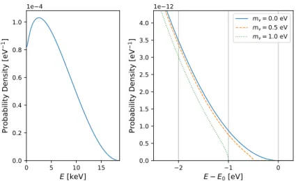
The Karlsruhe Tritium Neutrino (KATRIN) experiment determines the effective electron anti-neutrino mass by measuring the electron energy of the β-decay. The effect of the anti-neutrino mass on the electron spectrum is shown in figure 1.4.
The mass of the anti-neutrino shifts the endpoint energy of the spectrum to lower energies corresponding to the neutrino mass. Therefore, by measuring the region of the endpoint of the spectrum and comparing it to the expected spectrum without a neutrino mass, the effective neutrino mass of equation (1.4) can be determined.
KATRIN is designed to have a sensitivity of 200 meV at 90 % C.L. This is one order of magnitude better than the limits predecessors of KATRIN achieved [9, 28].
Improving by this much is only possible because of the high-luminous tritium source and an electron energy filter with an energy resolution below 1 eV.
A keV-sterile neutrino would have a similar effect on the β-spectrum as active neutrinos have, but because of the much bigger mass, the imprint would be visible deeper in the spectrum. The mixing of sterile with active neutrinos is expected to be extremely small. Therefore, to detect this imprint a lot of data is needed.
This makes the KATRIN setup with its high-luminous source very promising for the search for sterile neutrinos. For this reason KATRIN is explained in the first part of this section and afterwards it is shown how to detect a sterile neutrino in the β-decay spectrum.
1.3.1. Setup
KATRIN uses integral measurements of the β-spectrum. This means that the electrons, created in the source, are selected by their energy through a spectrometer.
All electrons above a certain energy is counted in the detector. This is done for different energies in a region around the endpoint of the spectrum. The setup of KATRIN is shown in figure 1.5. The experiment consists of five main parts.
1.3. KATRIN Experiment
0 5 10 15
E [keV]
0.0 0.2 0.4 0.6 0.8 1.0
Probability Density [eV1]
1e 4
2 1 0
E E0 [eV]
0.0 0.5 1.0 1.5 2.0 2.5 3.0 3.5 4.0
Probability Density [eV1]
1e 12
m = 0.0 eV m = 0.5 eV m = 1.0 eV
Figure 1.4.: Effect of the anti-neutrino mass on the β-spectrum endpoint. Left:
Differential spectrum of theβ-decay electrons. Right: The endpoint of the spectrum is shifted to lower energies according to the mass of the anti-neutrino. The endpoint without a neutrino mass is denoted byE0. Adapted from [35].
a) b)
c)
d) e)
a) Rear section
b) Windowless Gaseous Tritium Source (WGTS) c) Transportation section
d) Spectrometer section
e) Focal Plane Detector (FPD)
Figure 1.5.: KATRIN setup overview. Taken from [52].
Rear Section
The rear section’s main purpose is to supply an electric potential to the tritium plasma in the source by providing a conducting surface. This is done by a gold plated stainless steel disk, the rear wall. Also, calibration tools and monitoring devices for the tritium in the source are located here [10].
Windowless Gaseous Tritium Source
Tritium gas is continuously injected into a 10 m long and 90 mm wide steel tube, the Windowless Gaseous Tritium Source (WGTS). Inside the source the gas streams freely to both ends. There it is pumped out of the tube to be refurbished and then reinjected into the source. This way a tritium purity above 95 % is achieved. The decay rate is stabilized to 1011decays/s with a variation below 0.1 % [25].
Transport Section
In this section the residual tritium has to be reduced by 14 orders of magnitude.
Mainly turbo-molecular pumps are used for the reduction, but also cryogenic pumps with a small argon frost layer that traps tritium molecules. Further reduction is achieved by the chicane shape of the transport section. Electrons are guided adiabatically by magnetic fields, while molecules hit the walls and are then pumped away.
Spectrometer Section
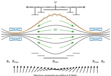
KATRIN uses two spectrometers to select the electrons that are counted in the detector. Both are built as Magnetic Adiabatic Colliminator and Electrostatic (MAC-E) high-pass filters, the principle is shown in figure 1.6. The electrons are guided by an magnetic field inside the spectrometer. Because of their momentum being not purely parallel to the field lines they perform cyclotron motion along the field lines. In the center of the spectrometer a high electric potential U is applied, the retarding potential. This field decelerates all electrons and rejects those with kinetic energies below qU. Because the cyclotron motion around the magnetic field lines, the energy of an electron Ee is split in a forward motion (parallel to the electric field lines) Ek and one perpendicular to the forward motion E⊥:
Ee=Ek+E⊥ (1.6)
The rejection through the electric potential acts only on Ek. To not falsely reject electrons which energy is mainly in the cyclotron motion, the magnetic field has its maximum strength at the beginning and the end of the spectrometer. The minimum
1.3. KATRIN Experiment
Figure 1.6.: Working principle of a MAC-E filter. Electrons are entering from the left.
A magnetic field with a gradient (black) shifts the electron momentum to be parallel in the middle of the spectrometer. In the center, also a high retarding potential is applied (green) to reject all electrons with energies below qU. Taken from [47].
lies exactly in the center, corresponding to the point where the electric potential is applied. This magnetic gradient reduces the cyclotron motion adiabatically, so that the momentum of the electron is shifted to be parallel to the field lines, in the middle of the filter (see bottom of figure 1.6). This way all kinetic energy is parallel to the electric field lines and no electron is falsely rejected. The energy resolution of the spectrometer can be calculated with equation (1.7) and is below 1 eV.
∆E
E = Bmin
Bmax (1.7)
After passing the filter, the electrons are accelerated and guided to the detector.
The KATRIN experiment uses an integral measurement technique. The retarding potential of the MAC-E filter is varied and all electrons above a set voltage are counted in the detector.
Focal Plane Detector
The Focal Plane Detector (FPD) is located at the end of the KATRIN beamline.
It consists of 148 pixels with 44 mm2 each, arranged in twelve concentric rings.
The layout is shown in figure 1.7. Each pixel is a pin-diode which is explained in
Figure 1.7.: Layout of the focal plane detector. It has 144 pixel and is segmented into twelve concentric rings. Each pixel has the same size. Taken from [47].
section 2.1 and records its own spectrum. The detector has a diameter of 90 mm. In front of the detector is an additional post-acceleration that increases the energy of the incoming electrons, because the detector efficiency is better for higher energies.
The energy resolution of the detector is about1.5 keV, which is not of importance because resolution of the measurement is given by the MAC-E filter and the detector only serves as a counter. The maximum rate the detector and readout can handle is 62 kcps [25].
1.3.2. Sterile Neutrino in the β-Spectrum
The neutrino mass eigenstates (ν1, ν2, ν3) reduce the endpoint of the β-spectrum.
Another neutrino mass eigenstate ν4 would have a similar effect. This is shown, largely exaggerated, in figure 1.8. The β-spectrum is a superposition of all four mass eigenstate spectra. Therefore, the endpoint of the sterile neutrino spectrum would manifest itself as a kink in the summed spectrum. This influence can by described by:
dΓ
dE = cos2 dΓ
dE
mνe
Θ(E0−E−mνe)
| {z }
Active Neutrino
+ sin2 dΓ
dE
ms
Θ(E0−E−ms)
| {z }
Sterile Neutrino
(1.8)
1.3. KATRIN Experiment
0.0 2.5 5.0 7.5 10.0 12.5 15.0 17.5
E [keV]
0.0 0.2 0.4 0.6 0.8 1.0
Probability Density [eV1]
1e 4
ms
no sterile neutrino with sterile neutrino
Figure 1.8.: Effect of a sterile neutrino mass on the β-spectrum. A kink appears at an energy below the endpoint of theβ-spectrum corresponding the mass of the sterile neutrino. In this case a mass of 12 keV is shown.
Taken from [35].
E is the energy of the electron and E0 is the endpoint of the spectrum. Θ is the mixing angle between active and sterile neutrino and ms the mass of the sterile neutrino. The position of the kink is therefore at an energy of E0−ms.
The high-luminous tritium source of KATRIN is one of its main advantages which also makes it suitable for the search for sterile neutrinos. The tritium spectrum has an endpoint at 18.6 keV that would allow to look for sterile neutrinos up to this mass. With the source and spectrometer of the current KATRIN setup two measurement methods are possible. One is the integral method, that is also used in the search for the neutrino mass. Here, the spectrometer is set to different retarding potentials and the detector counts all incoming electrons. Another way could be a differential measurement in which the MAC-E filter is set to a very small retarding potential at all times. This way the entire part of interest of the spectrum reaches the detector. In both measurement methods the rate on the detector can increase up to around 1010electrons/s, which is too high for the current detector system. A sensitivity study showed that the statistical sensitivity achievable with the KATRIN source, for the mixing angles are sin2(Θ) = 10−9 to10−6 for sterile neutrinos [34]. This depends on the measurement method and can be seen in figure 1.9. The sensitivity study shows that the imprint of a sterile neutrino is stronger in the differential measurement method. With the WGTS of KATRIN up to 1020 decays are measurable in three years. This amount of data would lead to further improvements on currently existing laboratory limits [35]. To achieve this
Figure 1.9.: Statistical sensitivity for a keV sterile neutrino using the KATRIN source. The differential and integral denote different measurement methods. N is the number of measured electrons. The gray area is excluded by astrophysical observations. Taken from [34].
sensitivity a new detector system has to be developed that can handle the high rates necessary for the investigations.
1.4. TRISTAN Project
The current KATRIN detector is not suited to search for keV-sterile neutrinos because it cannot handle the high electron flux. A new detector system is needed for this kind of search. To develop this detector is the aim of the Tritium Investigation on Sterile (A) Neutrinos (TRISTAN) project.
Requirements for the Sterile Neutrino Search
To achieve a statistical sensitivity for the mixing angle of sin2(Θ)<10−6 and the mass ms <18.6 keV at least 1016 electrons need to be analyzed [35]. Assuming a measurement period of three years, the electron rate will be around 108counts/s on the detector. Handling such high rates requires the detector to have multiple pixels, which distributes the rate. Reducing the pile-up probability leads to a minimum of 1000 pixels. Furthermore, the read-out system of the detector has to be extremely fast to cope with the rates. Thus, the shaping time τ of the system has to be small.
Another requirement is the excellent understanding of the whole tritiumβ-decay
1.4. TRISTAN Project
spectrum. Probing the parameter space in regions of cosmological interest, an understanding on the part-per-million level is needed [34]. Therefore, the detector needs an energy resolution of 300 keV at30 keV and the detector response has to be precisely known. If the resolution is too big the kink-like structure is not visible in the obtained spectra.
The series noise of a detector system Qseries influences the energy resolution.
Equation (1.9) shows that the noise is correlated to the shaping time τ [49]:
Qseries= Cd
√τ q
4kBT Rs+e2ampl (1.9) The proportionality to the inverse of the shaping time shows that a balance between short shaping times and low series noise has to be found. All the other parameters:
the capacitance of the detector Cd, the noise of the signal amplifiereampl, the series resistance of the detectorRs, and the temperature T need to be as small as possible.
Here, kB denotes the Boltzmann constant.
Finally, the entrance window of the detector needs to be extremely thin. Electrons lose a significant fraction of their energy shortly after entering the material. If some or all deposited energy in the entrance window is lost, the resolution is worsened and the entire spectrum is shifted to lower energies. With a thin entrance window this effect is smaller. Because it is important to know the influence of the entrance window of the detector on the tritium spectrum, in this thesis the entrance windows of the TRISTAN prototype detectors (described in chapter 2) are characterized.
Also a new production technique for the detectors is investigated.
Final TRISTAN Detector
All of the requirements mentioned above can be achieved with a multi-pixel detector system of silicon drift detectors. Following a detailed Monte-Carlo simulation [27], the TRISTAN detector system will consist of around 3500 silicon drift detectors.
The working principle of the detectors is explained in section 2.1.2. Silicon drift detectors allow for extremely small capacities of Cd= 110 fF. Each pixel will have a diameter of 3 mm. They will be grouped into twenty-one modules with 166 pixels each, the design of one module is shown in figure 1.10. Each module consists of one silicon drift detector chip, one cooling block and the first electronics stage. The final system will have a diameter of around 18 cm, a drawing is shown in figure 1.11.
The current prototype detector with seven pixels will be discussed in more detail in chapter 2.
Figure 1.10.: Design of a TRISTAN module prototype. It consists of one 166 pixel silicon drift detector chip, a cooling block, and the first electronics stage. Taken from [46].
Figure 1.11.: Design of the final TRISTAN detector system made out of twenty-one modules. Taken from [46].
2. TRISTAN Prototype Setup
In this section, an overview of the current TRISTAN prototype detectors is given.
The first part describes the working principle of semiconductor detectors. Afterwards, the silicon drift detector (SDD) is described as it is the type of detector used in the TRISTAN project. Following that, the current prototype detector setup is depicted.
In the end, the readout chain of the experimental setup is explained.
2.1. Functional Principle of the TRISTAN Detector
2.1.1. Basic Principle of Semiconductor Detectors
The working principle of semiconductor detectors depends on the band structure of the used materials. In contrast to metals, in semiconductors there is an energy gap between the conductive band and the valence band but it is not as big as in insulators. This means that electrons in the valence band can be excited to cross the gap and enter the conductive band. Therefore, semiconductors are able to conduct electricity but not as well as metals do. The different band structures of metals, semiconductors, and insulators is shown in figure 2.1.
A semiconductor’s conductivity is temperature dependent, as close to absolute zero nearly no electrons have enough energy to be in the conductive band. However, the higher the temperature of the material, the higher the chance to thermally excite electrons into the conductive band.
A widely used semiconductor detector material is silicon because it is one of the most abundant elements in the earth’s crust [56], and has a band gap of about 1.1 eV at room temperature [22]. Thus, the energy to create one electron-hole pair ω = 3.64 eV is fairly low [37]. Therefore, many electrons are created and able to enter the conductive band per deposited energy. This leads to a better energy resolution compared to other semiconductor materials.
To modify the conductive behavior of the semiconductor it is also possible to dope it with other materials, by adding other materials additional energy levels can be created inside the gap. Thus, the necessary energy for excitement is lowered.
This process also creates free electrons or free holes. There are two ways to achieve this for silicon, a type IV element. The first is to dope the semiconductor with
Figure 2.1.: Schematic drawing of the band differences of insulators, semiconductors and metals. The energy gap between valence and conductive band in insulators is too big for electrons to cross. In semiconductors the gap is small enough that some electrons may be excited, thermally or otherwise, to enter the conductive band. Metals do not have a gap and the bands can even overlap. Therefore, they are always conductive. The Fermi energy is shown to indicate the maximum energy non-excited electrons can have.
type V material, e.g. phosphorus. This creates an n-type semiconductor with an energy level close to the conductive band. Hence, even for low temperatures there are some electrons inside the conductive band. The other way is to add type III elements, e.g. boron. This leads to p-type semiconductors with an additional energy level close to the valence band. Consequently, free holes are created in the valence band, as electrons enter this new energy level. These two doping types are shown schematically in figure 2.2.
Incoming particles deposit energy and create electron-hole pairs. The number of those is usually several orders of magnitude lower than the number of free charge carriers at room temperature in an intrinsic silicon substrate. Thus, the signal would be lost in thermal noise. To prevent that and to be able to use a doped silicon substrate as a particle detector, the free charge carriers have to be reduced drastically [21].
To do so, the silicon volume is depleted of free charges by using a reversed-bias pn-junction. The operating principle of such a junction is shown in figure 2.3. A pn-junction is the combination of a p- and an n-type semiconductor. The excess electrons of the n-type material move to the p-type material while the surplus holes of the p-type move to the n-type. Therefore, recombination happens and charged dopant atoms are created until an equilibrium is established (figure 2.3b).
This results in an electric potential, the so-called diffusion voltageUdiffusion. In the transition area of the two types no free charges exist. This area is called depletion
2.1. Functional Principle of the TRISTAN Detector
Figure 2.2.: Schematic drawing to illustrate n- and p-type doping mechanisms.
Left: n-type semiconductors have additional energy levels close to the conductive band. Hence, even at low temperatures electrons enter the conductive band. Right: The p-type semiconductors have another energy level close to the valence band. Therefore, for every dopant atom, one or more electrons have this energy, which leaves free holes in the valence band.
zone, shown in figure 2.3c [21].
Applying an external voltage Ubias, which has the same polarity as Udiffusion, increases the depletion zone. Thus, the whole pn-junction becomes completely depleted (figure 2.3d).
Particles entering the material lose energy and create electron-hole pairs. If this happens in the depletion zone, recombination cannot happen. Hence, due to the electric field, all created electrons drift to the n-type part, the anode, where they are read out. The signal’s amplitude is proportional to the deposited energy. The holes similarly move to the p-type part.
This detector type is called a positive-intrinsic-negative diode (pin-diode).
2.1.2. Working Principle of an SDD
The first working silicon drift detector was introduced by Rehak and Gatti [42].
It is based on the principle of sideward depletion and depends on a small anode capacitance [29]. It is most suitable for measurements of X-rays and charged particles.
(a) (b)
(c) (d)
Figure 2.3.: The implementation of a pn-junction is illustrated by several steps.
In figure (a), the n-type semiconductor with additional electrons is shown in blue and the p-type with additional holes is shown in red.
When the two types are combined, figure (b), recombination happens at the contact area as electrons drift from the n-type part into the p-type one and vice versa for the holes. Therefore, the gray depletion zone of figure (c) is created, without free charges. This also builds the internal diffusion voltage which stops any further recombination. If an external potential in the direction of the diffusion voltage is applied to the junction, the complete detector can be depleted, as shown in figure (d).
2.1. Functional Principle of the TRISTAN Detector
(a) (b)
(c) (d)
Figure 2.4.: The steps necessary to get from a pin-diode to an SDD are shown in figures (a) to (d). It starts with a pn-junction where the ohmic contacts for the n+ anode (blue) and the electrode (red) cover the whole surface of a detector on each side and some voltage U is applied to the p+ electrode . In this illustration, U is lower than the bias voltage Ubias, necessary to deplete the whole volume. The same result as in (a) can be achieved if the anode is mostly replaced by additional p+ electrodes, which also have to be supplied by voltage U. Applying Ubias results in a nearly complete depletion of the detector, as shown in (c). But thereby only electrons close to the anode are directed towards it, as most electric field lines are perpendicular to the surface and do not point in the direction of the anode. An electric potential may be established in the detector which has its minimum at the position of the anode. To do so, the p+ electrodes on the anode side need to be replaced with electrode strips, on which gradually decreasing voltages from Uout to Uin are applied. Thus, all electrons inside the depleted part of the SDD drift to the anode (d). Pictures adapted from [47].
The working principle of an SDD is explained in figure 2.4. In figure 2.4a the ohmic n+layer covers one side of the diode. By applying an external voltage U some area around the p+ layer is depleted. A similar depletion can be achieved if the n+ is, except for a small area, exchanged by p+, which is shown in figure 2.4b. If now the voltage U is increased to the bias voltageUbias, the whole detector volume is depleted. The n+ takes the role of the anode and all p+ layers are cathodes. In this configuration, only one fourth of the potential is needed compared to a pin-diode with the same area and volume [11].
With the design in figure 2.4c, the electric field is mostly perpendicular to the surface. Therefore, only electrons close to the area above the anode are guided to the latter. By replacing the p+ areas on the anode side of the detector by an array of strips and applying decreasing voltages from Uout to Uin to each strip, a field parallel to the surface is established. The electrons drift to the n+ due to the resulting electric field which has its minimum at the anode. This is illustrated in figure 2.4d. A simulation of such a field can be seen in figure 2.5. In this simulation, the equipotential of the area p+ is shown in the back and the field strips with their step-like negative potential are shown in the front.
As practically no electrons are lost in an SDD, the whole charge cloud of an incoming particle can be measured. Therefore, the pulse height of the output signal is proportional to the deposited energy.
The most important advantage of SDDs over pin-diodes is the small capacitance of the anode. In SDDs it is in the order of 100 fF and practically independent of the active area of the detector. This is important as it reduces electronics noise and allows for small shaping times during signal processing [11].
Usually in particle physics, linear or matrix-like SDDs are used. But also radial designs exist as shown in figure 2.6. The radial design has the advantage that in this configuration it is much easier to terminate the field lines [29]. The potential is radial symmetric because the p+-electrodes are circular and are called "drift rings".
Therefore, the electron cloud is guided to the middle of the detector where the anode is located.
2.1.3. Influence of the Entrance Window on Particles
Unlike photons, electrons continuously lose energy when traveling through matter.
Their high interaction rate with the material is due to their charge. Therefore, they create secondary electrons and holes on their way. Due to the spatial expansion of the p+ doping, the electric potential inside the detector material, i.e. inside the bulk, is not the same as on its surface. This leads to a different behavior of electrons created on the surface compared to inside the bulk [31, 40]. Electrons do not drift towards the anode but diffuse in an uncontrolled way.
2.1. Functional Principle of the TRISTAN Detector
Figure 2.5.: Simulation of the resulting electric potential inside an SDD. In the back is the homogeneous potential of the entrance window. The front shows the step wise decreasing potential of the strip electrodes. Therefore, the anode is at the minimum potential. Taken from [29].
Figure 2.6.: Radial design of an SDD. The p+ back contact is the entrance window of the detector and has the same doping as the drift rings in red. Taken from [47].
There are effects that also lead to charge losses. One contribution is the silicon oxide on the detector. In this layer no deposited energy is detected. This SiO2 is always present as it results when silicon is exposed to air. By adding such a layer before it naturally grows, it can be created as homogeneously as possible and also protects the detector from further oxidation [47]. For the TRISTAN detectors this layer is usually 8 to 10 nm thick. Behind this is a volume of incomplete charge collection because of the expansion of p+.
The easiest way to describe this behavior is the sharp edge dead layer model. For this it is assumed that the entrance window of the detector is completely insensitive followed by a complete charge collection. A slightly advanced version of this is by assuming the silicon oxide is completely dead and afterwards a "washed-out" step function with a position and a spread describes the shape of the charge collection efficiency (CCE). This takes into account that events that deposit energy close to the entrance of the detector create charges which are partly lost. Therefore, the energy cannot be measured completely. In this thesis both of these models are used.
For the characterization of TRISTAN prototypes a sharp edge dead layer will be used. These detectors have been highly optimized for the detection of electrons and thus a thin dead layer is a reasonable assumption. In the second part of this thesis a washed-out step function will be used because the investigated pin-diodes are not optimized for electrons.
A common approach of testing if such models fit real experimental results is by using Monte-Carlo simulation software. Geant4 is a toolkit developed at CERN and widely applied in high energy, nuclear, medical, and accelerator physics. It is implemented in the C++ programming language [8]. With this a wide range of particles and materials can be simulated. Also different interaction mechanisms like electromagnetic or hadronic can be taken into account. Additionally, the properties to take into consideration and which to neglect can be chosen. Its variety of possible applications make it suitable to simulate the detector response of the TRISTAN prototypes to the emitted conversion electrons and photons of the 83mKr decay.
The description of electrons in the silicon detectors for the KATRIN experiment with Geant4 was not precise enough. Therefore, a new software called KESS was developed. The aim was to model especially the energy loss of low-energy electrons, the energy deposition, and the production and tracking of secondary electrons in silicon very precisely [43]. For this reason it is used to simulate the response of pin-diodes to incoming electrons at different energies, especially in the range of 1to 2 keV. This is used in chapter 4 of this thesis.
2.2. TRISTAN Prototype Detector
2.2. TRISTAN Prototype Detector
The prototype detectors of the TRISTAN project are silicon drift detectors with a thickness of 450µm. The prototype’s pixels are not circular (as described above) but hexagonally shaped. This gives all benefits of the radial design, but additionally allows for pixel arrays without gaps and therefore increases the maximum coverage area. The diameter of a pixel is 2 mm. The arrangement of pixels is shown in figure 2.7.
The bias voltage needed to fully deplete the detector is called back contact voltage.
It is Ubias =UBackC=−90 V. This is applied to the p+-doped side of the area on the entrance window. To prevent electrons created inside the pixel from leaving and guarding it from outside electrons, an additional p+-guard-ring surrounds the detector. It is called back frame and is set to Ubackframe =−100 V. The entrance window and the contact points are shown in figure 2.8.
The electric field guiding the electrons to the anode in the center of each pixel is created by twelve drift rings on the electronic side of the detector. The gradient between each ring is given by the difference of potentials of the outermost ring Uringx = −110 V and the inner most ring Uring1 = −20 V. The anode, shown in figure 2.7, has a diameter of 90µm and therefore a capacitance 110 fF. The connection to the first amplification stage is an aluminium bond with18µmdiameter.
With this, the capacitance is hardly increased and additional noise can be reduced.
The first amplification is done by the low noise preamplifier application-specific integrated circuit (ASIC)-CUBE [12]. These ASICs are positioned close to the anode around the pixels. The setup of CUBEs can be seen in figure 2.7.
After the first amplification the signal is routed through the detector printed circuit board (PCB) to the output pins. The board also handles the rewired power supply for the ASICs and the detector.
For the TRISTAN project, several detectors with different entrance windows have been produced. To distinguish them the naming scheme of table 2.1 was developed.
The first two letters describe the doping profile used for the detector. The number is an integer increasing with every new detector of a kind.
The standard entrance window doping profile is not TRISTAN specific [40] and highly optimized for photon detection. To further decrease the thickness of this ultra thin entrance window other doping profiles are tested. One technique is to lessen the dose of implants during the process. This reduces the p+-doping and therefore the depth to which the dopant atoms enter the detector, as shown in figure 2.9. The advantage is that it shifts the electric fields maximum closer to the surface (figure 2.9). But it increases the risk of not fully depleting the detector. This is tried for the R0 detectors. An alternative is to implant n+ behind the p+ doping.
This again has the risk of not fully depleting the detector if the dopings are not