DEPMOSFET Active Pixel Sensor Prototypes for the XEUS Wide Field Imager
J. Treis, P. Fischer, O. H¨alker, M. Harter, S. Herrmann, R. Kohrs, H. Kr¨uger, P. Lechner, G. Lutz, I. Peric, M. Porro, R. H. Richter, L. Str¨uder, M. Trimpl and N. Wermes
Abstract— Active Pixel Sensors (APS) based on the DEPMOS- FET (Depleted P channel MOSFET) recently produced at the MPI semiconductor laboratory are a promising new type of sensor to cope with the advanced requirements of the XEUS Wide Field Imager, a large area imaging and spectroscopy detector for X-ray astronomy. DEPMOSFET APS combine high energy resolution, low power consumption and random accessibility of pixels providing for highly flexible readout modes with fast readout speed. In the first prototype production, several design variants of 64 x 64 pixel DEPMOSFET matrices with a pixel size of 75µm× 75µm have been realized. A Data Acquisition system (DAQ) for evaluation of sensor prototypes has been developed, which allows for a performance characterization of the different designs. For operation, DEPMOSFET device, front-end IC and control ICs are integrated onto a readout hybrid. Device readout is done row by row, addressing and resetting one single matrix row at a time and processing the signals with a 64 channel parallel CMOS amplifier / multiplexer IC of the CAMEX type applying 8-fold correlated double sampling. Addressing and resetting of the matrix rows is done by two control ICs of the SWITCHER type fabricated in a high voltage CMOS technology. A number of readout hybrids has been built, the characterization of the different devices in terms of noise, spectral resolution and charge collection efficiency is in progress. The most promising DEPMOSFET matrix design variants, the DAQ system and measured key performance parameters of the devices are presented.
Index Terms— XEUS, X-ray, DEPFET, Active Pixel Sensor, Imaging, data acquisition, spectroscopy.
I. INTRODUCTION
F
ROM their introduction in 1987 [1], Active Pixel Sensors based on the DEPFET principle were subject to intense studies [2], [3]. Several prototypes have been manufactured and evaluated, and DEPFET APS based sensors turned out to be a promising new concept for both imaging applications and high resolution X-ray spectroscopy. Due to the latest advancements of technology [4], large-area APS sensors using DEPFETsManuscript received November, 4, 2004
J. Treis, O. H¨alker, S. Herrmann and L. Str¨uder are with the Max-Planck- Institut f¨ur extraterrestrische Physik, MPI Halbleiterlabor, Giessenbachstraße, D-85748 Garching, Germany (e-mail: jft@hll.mpg.de).
P. Fischer, M. Harter and I. Peric are with Mannheim University, Institut f¨ur technische Informatik, D7 2-4, D-68159 Mannheim, Germany.
R. Kohrs, H. Kr¨uger, M. Trimpl and N. Wermes are with Bonn University, Nußallee 12, D-53112 Bonn, Germany.
R. H. Richter and G. Lutz are with the Max-Planck-Institut f¨ur Physik, MPI Halbleiterlabor, F¨ohringer Ring 6, D-80805 Munich, Germany.
P. Lechner is with PNSensor GmbH, R¨omerstraße 28, D-80803, Munich, Germany.
M. Porro is with Politecnico di Milano, Dipartimento di Elettronica e Informazione, Via Golgi 40, I-20133 Milano, Italy.
have now come within reach. Thus, a design concept for the Wide Field Imager (WFI) [5], [6] of the X-ray Evolving Universe Spectroscopy (XEUS) [7], [8] mission was proposed, which consists of a single large area monolithic DEPFET array surrounded by a ring of MOS CCDs. The DEPFET device will have a total area of 76.8 mm×76.8 mm, which is divided into 1024×1024 pixels of 75 µm×75µm size each [9]. It will be integrated onto a single 6” wafer of 450µm thickness. The required energy resolution is 125 eV at the Mn-Kαenergy and 50 eV at the C-Kα energy. Pixel size and energy resolution provide for a spatial resolution of 30 µm. A frame rate of 1 kHz is required. The overall power consumption of the sensor is required to be below 1 W.
A production of DEPFET sensors including sensor pro- totypes for XEUS has recently been finished at the MPI semiconductor laboratory in Munich. The technology developed for that purpose provides two polysilicon and up to two metal layers, which make self-aligning implantations and highly- flexible metal interconnections possible. In addition, the new DEPMOSFETs use MOSFETs with polysilion gates as ampli- fying transistors instead of the JFETs used in earlier devices, which improves the homogeneity of the sensor. These features greatly increase the scalability with respect to future large-area devices.
First measurements on single pixel DEPMOSFET structures, which were presented elsewhere [9], [10], showed excellent results. Here, the concept of the DEPMOSFET matrices, the different design variants, the readout system and results of prototype device tests are described.
II. DEPMOSFETDEVICES
A DEPMOSFET (DEpleted P-channel MOSFET) consists of a p-channel MOS-field effect transistor integrated on the surface of a high resistivity n-type silicon bulk. Making use of the principle of sideways depletion [11], the bulk can be fully depleted using the reversely biased p+-doped backside diode, the p+-doped source and drain contacts of the FET and the remote n+-type bulk contact. By applying appropriate bias voltages, a parabolic potential distribution with a potential minimum for electrons close to the upper surface of the bulk is generated. This minimum can be confined further in lateral di- rection to the area below the transistor channel by an additional n-doped region. This implantation also increases the depth of the potential minimum. Electron-hole pairs generated in the
Fig. 1. Cutaway and circuit schematic of a circular DEPMOSFET pixel. The pixel consists of a circular p-channel MOSFET with attached clear region, which can be considered as an additional ’parasitic’ n-channel MOSFET contacting the internal gate. The circular polysilicon gate has a width of 5 µm and a circumference of 47.5µm.
silicon bulk are separated by the electric field. While the holes drift to the backside contact, the electrons are collected in the potential minimum below the transistor channel, modifying the charge carrier density in the channel by inducing an additional amount of holes. Thus, the channel conductivity is a function of the amount of charge in the potential minimum, which is therefore called internal gate.
As the internal gate is capable of storing signal charges regardless of the presence of a transistor current, the transistor current can be turned off during signal integration to reduce power consumption. However, the internal gate fills up with charges during operation in integration mode until a dynamic equilibrium state is reached, in which charge is lost to the most positive contact nearby. Thus, to prevent the internal gate from losing its charge storage capability, the accumulated charge has to be removed regularly by applying a positive voltage pulse to the so-called clear-contact, an n+-doped region close to the internal gate.
For the sake of improved charge collection and a more efficient filling of the pixel area, the DEPMOSFET structures designed as prototypes for the XEUS WFI have circular transis- tor geometry. The clear region here consists of the clear contact and a surrounding MOS structure, the so-called cleargate. The clear contact is additionally separated from the detector bulk and the internal gate by a deep p-implanted well. Clear and cleargate together can be considered as an additional n-channel MOSFET connecting clear and internal gate. Figure 1 shows a cutaway of a circular DEPMOSFET structure.
The DEPMOSFET structures for XEUS are designed for source follower readout. Here, the pixel source contact is biased by a constant current source. A change in the MOSFET channel conductivity yields a voltage step at the source node propor- tional to the amount of charge collected. As the complete clear provides for a reproducible baseline, comparing the voltage
Fig. 2. Simplified interconnection scheme of pixels on the DEPMOSFET matrix protoypes for XEUS. All pixels have a common drain contact. The gates, cleargates and clear contacts are connected row-wise, while the pixel sources are connected column-wise. Every source column is biased by a column- individual current source, which is provided externally.
levels at the source node of the pixel before and after the clear process provides the signal information. In the first approach, the relation between the charge in the internal gate and the resulting voltage step at the source node can be estimated to be:
vs = gq
gm ·∆Qs, (1) where gm is the transconductance of the DEPMOSFET’s ex- ternal gate,gq the so-called charge transconductance, which is the ratio
gq = δIpixel
δqint. gate
, (2)
and∆Qsthe amount of signal charge removed from the internal gate during the clear process.
For building large area sensors with DEPFET pixels, a pixel array is integrated onto a single die with common bulk and back contact. By applying a suitable interconnection scheme between the individual transistor terminals, groups of pixels can be formed and randomly accessed.
For the current DEPMOSFET structure prototypes, a simple interconnection scheme has been chosen, which is shown in figure 2. All matrix pixels are connected to a common drain.
Gate, clear and cleargate contacts are connected row-wise and the sources of all transistors within one pixel column are connected as well. For the source follower mode operation, every column is contacted by an external current source. By applying appropriate voltages to the gate contacts, only a single row of pixels can be turned on. Thus, voltage changes at the column-individual source node are due to changes of the internal gate fill level of the pixel in the row which is currently active.
Matrix readout is done row-wise, i.e. the signal information of all pixels in a row is processed in parallel. All pixels integrate signal charges for a fixed time interval. For readout, the transistor currents in the respective row are turned on via the external gate voltage. The voltage level at the source node
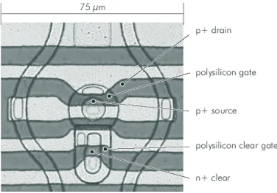
Fig. 3. Microscope photography of a DEPMOSFET pixel (cut gate structure type). The circular polysilicon gate has a width of 5µm and a circumference of 40µm. The bright horizontal lines are the metal connections of drain, gate, clear and cleargate. The source is connected in vertical direction by the curved polysilicon lines.
is read out. Next, the clear operation is performed in the row by using the clear and cleargate contacts. The voltage level at the source node now corresponds to the baseline information, the pixel signal with empty internal gate. The charge information can be obtained from calculating the voltage difference before and after the clear, and the transistor current in this row can be turned off. Then, the process is repeated in the next row.
Thus, the overall time the pixels in one row integrate the signals corresponds to the time needed to read out all other rows in the matrix.
The XEUS DEPMOSFET matrix prototypes consist of arrays of 64×64 pixels of 75µm×75µm size. The most favored structures have by design a nominal gate width of 5 µm.
The circular transistor gate has a circumference of 47.5 µm.
The internal gate geometric size and doping concentration are dimensioned to store more than 105 electrons in a pixel, a storage capability which is sufficient for most applications and which has been confirmed by measurements. For the current structures, gq-values of ≈ 200 - 300 pA / e− have been measured, depending on parameters like implantation profile and effective channel length. Figure 3 shows a microscope photography of a matrix pixel. The devices have been processed on 450µm thick wafers with a bulk n-doping of1−2×1011 cm−3, resulting in a depletion voltage between 30 to 150 V, depending on the individual wafer.
III. READOUT HYBRIDS
For evaluation, a prototype matrix is integrated together with the required front end ICs and additional filter circuitry onto a hybrid carrier. For switching the gate, cleargate and clear voltages, the SWITCHER II IC is used; the analog front end IC is the so-called CAMEX 64G. Figure 4 shows photographs of fully assembled readout hybrids. A detailed description of the front-end electronics can be found in [12].
The SWITCHER II is a 64 channel, dual output, high voltage switching circuit manufactured in an AMS high voltage CMOS process. It has been designed for the purpose
Fig. 4. Left: Close-up of the central area of a hybrid, with the sensor (middle), the Clear switcher (right), the Gate switcher (left) and the CAMEX IC at the lower edge of the sensor. The wire bond interconnections between the different ICs are visible. Right: Overview over a PCB type hybrid with the connector pins to the peripheral readout electronics and a coin showing the proportions.
of DEPMOSFET matrix readout. The IC provides two outputs for every channel, which can be toggled between two individual voltages each, and both an integrated sequencer and a direct timing mode for precise timing of the switching process. The total switch voltage difference can be as large as 20 V. During normal operation, the IC switches through the channels consecutively in an selectable direction and provides facilities for easy integration of a number of SWITCHER ICs to a daisy chain in case large sensor arrays have to be read out. As three voltage channels are to be switched during matrix operation, two SWITCHER ICs are operated on a single hybrid. The clear behavior of DEPMOSFET structures with respect to voltage levels, sequence and timing of clear voltage pulses has been studied on single pixel structures [10], and the parameter window where complete clear is possible has been determined.
The CAMEX (Charge Amplifier MultiplEXer) 64 G is a 64 channel parallel voltage amplifier with an 8 fold correlated double sampling (CDS) stage and serial analog readout. Here, signal acquisition in each channel is done by calculating the difference between the mean value of 8 samples taken before and 8 samples taken after the clear. The sampling process takes place for all 64 channels in parallel. It is a variant of the CAMEX family [13], which has been adapted to the requirements of DEPMOSFET pixel readout. It has a PMOS current source integrated in every channel for proper biasing of the source-follower operated pixel columns. Additionally, the timing of the various switch processes during CDS is generated by a built-in shift register sequencer allowing for very flexible signal shaping schemes. The analog signal voltage information is read out using a sample & hold in combination with a serializer circuit. The CAMEX sequencer can be operated at clock speeds of up to 10 MHz. At the moment, the minimum processing time for one row is about 12µs. A detailed discussion of the CDS filter properties of the CAMEX CDS filter and the influence of sample timing and amplifier bandwidth on the filter efficiency can be found in [14].
IV. PERIPHERAL READOUT SYSTEM
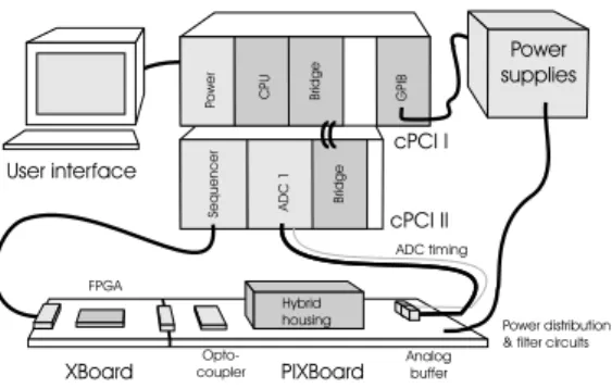
Figure 5 shows a simplified schematic of the peripheral readout system. A more detailed description can be found
Fig. 5. Simplified schematic of the system setup. A cPCI CPU controls the sequencer card and the DAQ ADC card. The control sequence is transferred via the XBoard to the PIXBoard, which holds the hybrid and performs galvanic decoupling, level shifting, bias generation and distribution and filtering for the required operation voltages. The analog output signals of the hybrids are transferred to the ADC card, which digitizes and formats the data.
in [12]. The setup is controlled by a cPCI CPU running the Windows XP operating system. All digital signals required by the readout system are generated by the sequencer, which is a commercially available cPCI pattern generator. In addition to its 16 bit fast pattern generator capability, it provides an interface for the software controlled slow control and configuration protocol.
An additional digital interface, the XBoard, was inserted between sequencer and hybrid. The XBoard (XILINX-Board) is an FPGA based multi-purpose digital interface card. It was added to the setup to overcome certain limitations of the sequencer card and to increase flexibility in readout timing. The so-called PIXBoard (PIXel Board) decouples the inner circuits of the setup galvanically from XBoard and sequencer card and holds the readout hybrids within an electrically shielded, light- tight housing. In addition, it provides digital and analog driver circuitry and all supply and bias voltages and currents required by ICs and sensor on the readout hybrid.
The ADC board is designed for acquisition of DEPMOSFET matrix data with high frequency. It consists of a commercially available cPCI base board equipped with a custom made piggy- back card holding a commercially available 14-bit ADC. An effective ADC resolution of 11.7 bit can be achieved with this system. Various control signals allow for storage of data in a frame-compatible format. The cPCI ADC has DMA capability, the acquired data is transferred to the PCI main memory via fast DMA. The system can handle a data rate of 40 MByte/s; at the current operation speed, the system has to cope with a data rate of 5 MByte/s only. To avoid interference from the CPU, sequencer and ADC card are located in a separate cPCI rack and are connected with an optical cPCI-bridge. A cPCI-GPIB interface permits control of the system power supplies. Control over ADC card and sequencer is possible using two independent C++ applications. The system is modular and scalable and can thus be adapted easily to larger sensor array sizes.
V. PROTOYPE DESIGN VARIANTS
As the DEPMOSFET device is an entirely new type of sensor produced in a newly developed technology, the development
could not benefit from experience from precursor productions.
Therefore, several prototype designs are included in the produc- tion varying important design parameters, the most important of which are listed below. All those structure types are currently under study to find the most favorable design.
A. Standard vs. relaxed
For the standard pixel cell size of 75 × 75 µm2, two different DEPMOSFET transistor sizes have been implemented, the standard size with 5 µm gate width and 47.5 µm gate circumference and the so-calledrelaxed size with 7.5µm gate width at 65µm gate circumference. The latter was designed as fall-back solution in case of problems with the lithography for the standard pixel size. Relaxed sized structures are expected to have a ca. 30 % lower gq due to the increased gate length.
B. P1 vs. P0
The clear behavior of the pixel strongly depends on size and shape of the deep p, which shields the clear contact in depth and in lateral direction (see fig. 1). Especially the spatial overlap with the cleargate is important. If the overlap is too large, the voltages required for complete clear increase drastically; if the lateral size is too small, charge loss to the clear contact might result. For the P0 type structures, the deep P is aligned edge-to- edge with the clear contact; for P1 structures, the lateral overlap is about half the cleargate width.
C. Cut gate vs. round gate
The geometry of the contact area between gate and clear structure is expected to be of relevance for charge collection and clear behavior. Two versions have been realized. For the cut gate structures, the cleargate contact intersects the circular shape of the gate, as shown in fig. 3. For the round gate structures, the circular shape of the pixel gate remains unchanged, and the cleargate structure is itself intersected.
D. Enhancement vs. depletion mode
For some of the structures, depletion mode DEPMOSFETs have been used by adding an additional weak shallow-p im- plantation in the transistor channel region. Threshold voltages are thus shifted towards more positive voltages. This was done to achieve a better 1/f noise characteristics and a gate voltage range, which is easier to handle.
E. HE vs. non-HE
For some of the wafers, an homogeneous, high energetic deep n-implant was added to ease the clear and reduce the effect of parasitic hole currents to the backside. HE structures are additionally expected to be more insensitive to charge loss.
This is achieved at the cost of a reduced gq, which is by a factor of 1/3 lower than for non-HE structures.
F. Drain center vs. source center
The position of drain and source can be exchanged, which has influence on the design topology, but also on the clear behavior, as the outside transistor terminal determines the potential of the area surrounding the clear contact.
G. Single vs. double metal
To implement more advanced pixel interconnection schemes, more advanced routing capabilities are needed than provided by the initial single metal / double poly technology. In addition, connection lines carrying medium to high currents, for instance the column-common source contact, experience voltage drop in column direction when made in polysilicon, which might result in inhomogeneous operating conditions over the matrix.
Devices manufactured in a double metal process recently de- veloped do not suffer from these limitations.
VI. RESULTS
At the moment, evaluation of the various design prototypes is still in progress. All devices tested so far have been found to be homogeneous and defect-free. The following preliminary conclusions have been drawn from the data currently available.
• The pixels in standard size work as expected. No relaxed sized structures have so far been examined.
• P0 pixels are preferred, as P1 pixels need, for complete clear, voltages of 20 V or even higher. Additionally, charge loss into the clear does not seem to show up for the P0 pixels at the present state of evaluation.
• So far, no significant difference in performance has been observed between round an cut gate structures. Differences are expected to show up when so-called mix-structures will be operated, which are matrices incorporating both types of transistor on the same die. In this way, the differences in performance can be studied for the same biasing conditions.
• Drain center matrices are preferred, as charge losses are observed for source center matrices. These are most likely caused by a parasitic potential minimum underneath the clear contact, which could not be eliminated so far by optimization of the operating conditions, and which is not present for drain center structures.
• In addition to the increased homogeneity, double metal structures were found to have by a factor of 2 lower noise at room temperature compared to single metal structures of the same design. We explain this observation with the decrease of line resistance, when long polysilicon connections are replaced by aluminum lines.
• Few structures from HE wafers have been tested so far.
This will change as soon as the first HE wafer in double metal technology is about to be diced.
The structure performing best so far is a standard, depletion mode, cut gate, non-HE structure in double metal technology.
The measurements shown in the following have been made with this type of structure in a dried air atmosphere inside a
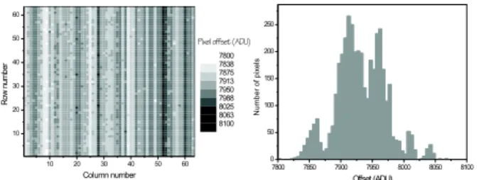
Fig. 6. Offset map of a DEPMOSFET matrix. The map shows a column-like structure, which has its origin in the intrinsic CAMEX channel offset and the CAMEX channel gain variation.
Fig. 7. Residual offset map of a DEPMOSFET matrix. The residual offset map can be obtained from the raw offset map of the CAMEX by subtracting common column and common row offset contributions. The matrix shows no bright pixels.
climate chamber for a detector temperature of -40◦C at a source follower current of 25µA per pixel. The frame rate was 300 Hz and the shaping cycle time for one row was≈15µs.
A. Offset
An offset map of the matrix is shown in figure 6. The overall offset distribution width is at the order of 2% of a Mn-Kα signal, so the offset does not reduce the dynamic range space. The offset map shows a prominent column-like structure. The offset signal consists of the CAMEX offset plus the respective pixel leakage current signal amplified with the respective channel gain. Thus, the observation of a column- like structure is expected, as the CAMEX shows a column- individual offset and a slight column-to-column gain variation.
The resulting distribution superimposes the original pixel offset variation due to pixel-individual gain and leakage current. The evaluation of the effective pixel offset distribution, showing inhomogeneities or bright pixels on the matrix itself, is possible, if the offset map is corrected with respect to the column structure by calculating the residual offset map, as shown in figure 7. After applying this correction, the residual distribution is flat and homogeneous. No bright pixels, pixels showing a leakage current significantly larger than the average, show up.
This has been found to be the case for all devices tested so far.
B. Gain
As every DEPMOSFET pixel has its own integrated first amplifier FET, the gain homogeneity is an important issue. The gain is calibrated by determining the Mn-Kαpeak pulseheight
Fig. 8. Gainmap of a DEPMOSFET matrix. The width of the gain distribution is about 3%. The mean gain of 1.25 ADU / eV corresponds to a source follower gain of 3.7µV / e−, which is in good agreement with the simulations.
The distribution column-like structure originates in the CAMEX channel gain variation.
Fig. 9. Noise map of a DEPMOSFET matrix. The dispersion of the noise distribution is at the order of 10% of the peak value. The mean noise of 13 eV corresponds to an equivalent readout noise charge of 3.6 e−ENC.
from the calibration spectrum for every pixel. To avoid inter- ference from charge splitting, the calibration spectrum is built from events which show no charge splitting to neighboring pixels. These are determined by applying a pattern detection algorithm using a pixel individual threshold of 5×σNoise for seed pixels and 3×σNoise for pattern constituents within a 3 x 3 pixel area around the seed. For the current measurements, these settings result in an effective low-energy threshold of
≈70 eV. A typical gain map and gain distribution are shown in figure 8. The distribution shows the integral gain, which is the product of CAMEX column gain and pixel gain, which explains the column-like structure in the gainmap. No dead pixels, i.e. pixels with a significantly lower gain than the mean gain value, have been found. A mean source follower gain of 3.7µA / e− has been measured, which meets the expectations from pre-production simulations. The total gain inhomogeneity has been found to be as small as 3%.
C. Noise
Figure 9 shows a typical noise map and noise distribution of the matrix. The map is homogeneous, no systematic effects over the matrix area can be observed. Additionally, no noisy pixels, pixels showing a significantly higher noise than the average, show up. The gain map can be used to determine the electronics readout noise of the device in terms of equivalent noise energy or equivalent noise charge. The mean measured equivalent noise energy of the matrix of 13 eV corresponds to an equivalent noise charge of 3.6 e−; the noise dispersion is about 10% of the mean noise, and the mean S/N ratio is about 450 for the Mn-Kαenergy. These values match the expectations
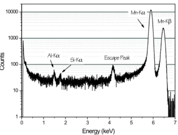
Fig. 10. Energy spectrum of an55Fe-source measured with a DEPMOSFET matrix while illuminating from the electronics side. The FWHM of the Mn-Kα peak is 131 eV, corresponding to an equivalent noise charge of 6.1 e−ENC.
Fig. 11. Energy spectrum of an55Fe-source measured with a DEPMOSFET matrix while illuminating the entrance window. The FWHM of the Mn-Kα peak is 133 eV, corresponding to an equivalent noise charge of 6.9 e−ENC.
from measurements of the DEPMOSFET pixel noise spectrum and measurements of the CAMEX frequency transfer function, which predict a readout noise of 3.2 e− ENC.
D. Spectral resolution
Figure 10 shows a spectrum obtained from a 55Fe-source while irradiating the device from the electronics side. The spectrum contains data from all pixels after gain calibration.
Again, the spectrum only from singles, i.e. photon events with no charge splitting, was taken to determine the energy resolution of the device. A very good spectral resolution is observed. The FWHM of the Mn-Kα-line is 131 eV, which corresponds to an ENC of 6.1 electrons. This is a little less than expected from the noise peak, as, for instance, charge collection effects and the remaining influence of split events have to be taken into account. All expected spectral features are clearly visible. The peak at the Al-Kαenergy is due to the presence of aluminum metal layers of the integrated electronics and an aluminum attenuator for the source.
The peak-to-background ratio is with≈500 not as good as expected, as the ”dead” layers from the integrated electronics cause an additional split fraction. The rise in count rate at the
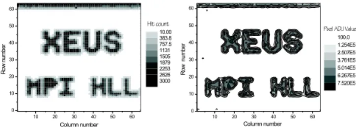
Fig. 12. Imaging measurement using a 300 µm thick silicon baffle. The smallest structure size was 150µm. Left: Contour plot from ADU maps. Right:
Hitmap applying a 100 ADU threshold.
low-energy range of the spectrum can not be explained by the width of the noise peak, as a 5σ-threshold was applied, and has to be investigated further.
Figure 11 shows a spectrum obtained from a 55Fe source while illuminating from the backside. Due to the short pen- etration depth of the X-rays and the large thickness of the wafer, which is 450 µm to increase the quantum efficiency for higher energies, few singles are observed compared to the frontside measurement. The ratio of split to non-split events is 0.4 for front side and 5.2 for backside illumination, which is in agreement with the expectations assuming some additional widening of the charge cloud in the weak drift fields close to the sensor surface. The measured energy resolution is 133 eV, corresponding to an ENC of 6.9 e−. This is a bit worse than for electronics side illumination; we explain this by the increased influence from residual split events.
The same device shows a spectral resolution at room temper- ature of 200 eV FWHM at the Mn-Kαpeak, corresponding to 18 e− ENC, for a readout noise of 16e−. At this temperature, the overall noise is dominated by the contribution from the leakage current.
When examining the energy resolution for patterns, the spectroscopic noise of the contributing pixels adds up. This leads to a deterioration of the energy resolution, which increases with the number of contributing pixels. For the double pixel patterns of the above frontside illuminated measurement, for instance, an energy resolution of 143 eV or 9.1 e- ENC has been measured, which is in agreement with the expectation.
E. Imaging capabilities
Figure 12 shows an imaging measurement made with a DEPMOSFET matrix using an 300 µm thick silicon baffle with a minimum structure size of 150 µm. Both ADU and a simple hitmap are shown. For the hitmap, an ADU threshold of 100 was applied, and for the ADU map all acquired frames were summed up. The measurements give an impression of the homogeneity of the device and show the suitability of the device for the use as an X-ray imaging detector. More detailed examinations of the imaging capabilities of the device including the spatial resolution are in progress.
VII. CONCLUSION
DEPMOSFET based active pixel sensors are considered to be suitable for the XEUS wide field imager. A prototype production has recently been finished and the evaluation process is still in progress. A number of readout hybrids has been built, including a complete set of control and readout electronics.
Additionally, a modular and scalable DAQ system has been set up, which serves for performance characterization of this and future prototype generations.
The devices show excellent homogeneity, and all devices tested so far are defect free. The suitability of the device for X-ray imaging has successfully been demonstrated.
The readout noise has been measured to be around 3.6 e− ENC at a detector temperature of -40◦C. For that temperature, the spectral resolution at an energy of 5.9 keV (Mn-Kα) has been measured to be 131 eV corresponding to 6.1 e− ENC.
The same device shows a spectral resolution of 200 eV at room temperature corresponding to 18 e− ENC and a readout noise of 16 e− ENC.
After finishing the characterization of the different proto- types, additional focus will be put on the optimization of oper- ation parameters to improve charge collection. Additionally, the readout timing will be improved. A new production, including devices of 256×256 pixels, will start in 2005.
REFERENCES
[1] J. Kemmer and G. Lutz, “New detector concepts,” Nucl. Instr. and Meth.
A, vol. 253, p. 356, 1987.
[2] P. Klein, G. Cesura, P. Fischer, G. Lutz, W. Neeser, R. Richter, and N. Wermes, “Study of a depjfet pixel matrix with continuous clear mechanism,” Nucl. Instr. and Meth. A, vol. 392, p. 254, 1997.
[3] P. Klein et al., “A depfet pixel detector system for the use in autoradio- graphy,” Nucl. Instr. and Meth. A, vol. 454, p. 152, 2000.
[4] R. Richter et al., “Design and technology of depfet pixel sensors for linear collider applications,” Nucl. Instr. and Meth. A, vol. 361, p. 250, 2003.
[5] X-ray Evolving Universe Spectroscopy-The XEUS Telescope. ESA SP- 1253: The XEUS Telescope Working Group, 2001.
[6] X-ray Evolving Universe Spectroscopy-The XEUS Instruments. ESA SP-1273: The XEUS Instrument Working Group, 2003.
[7] X-ray Evolving Universe Spectroscopy-The XEUS Science case. ESA SP-1238: The XEUS Astrophysics Working Group, 2000.
[8] X-ray Evolving Universe Spectroscopy-The XEUS Mission Summary.
ESA SP-1242: The XEUS Steering Commitee, 2000.
[9] L. Strueder et al., “Xeus wide-field imager: first experimental results with the x-ray active pixel sensor depfet,” in High-Energy Detectors in Astronomy, ser. SPIE proceedings, A. D. Holland, Ed., vol. 5501, 2003.
[10] P. Lechner et al., “Depfet integrated amplifiers for x-ray imaging and spectroscopy active pixel sensors,” in High-Energy Detectors in Astron- omy, ser. SPIE proceedings, 2004.
[11] E. Gatti and P. Rehak, “Semiconductor drift chambers-an application of a novel charge transport scheme,” Nucl. Instr. and Meth. A, vol. 225, p.
608, 1984.
[12] J. Treis et al., “First results of depfet based active pixel sensor prototypes for the xeus wide field imager,” in High-Energy Detectors in Astronomy, ser. SPIE proceedings, A. D. Holland, Ed., vol. 5501, 2004, pp. 89–100.
[13] W. Buttler, G. Lutz, V. Liberali, F. Maloberti, P. Manfredi, V. Re, and V. Speziali, “Evolution in the criteria that underlie the design of a monolithic preamplifier system for microstrip detectors,” Nucl. Instr. and Meth. A, vol. 288, p. 140, 1997.
[14] N. Hoernel, S. Herrmann, and M. Porro, “Filter performance of a multiple correlated double sampling system with finite reset,” IEEE transactions on circuits and systems II: Analog and Digital Signal Processing, vol.
(In preparation).