Active Pixel Sensors for Imaging X-ray Spectrometers
Peter Holl a,* , Peter Fischer b , Robert Hartmann a,* , Günther Hasinger c , Johannes Kollmer c,* , Norbert Krause c,* , Peter Lechner a,* , Gerhard Lutz d,* ,
Norbert Meidinger c,* , Ivan Peric b , Rainer Richter d,* , Heike Soltau a , Lothar Strüder c,* , Johannes Treis c,* , Joachim Trümper c , Norbert Wermes b
a PNSensor GmbH, Römerstraße 28, D-80803 München
b Physikalisches Institut, Universität Bonn, Nussallee 12, D-53115 Bonn
c Max-Planck-Institut für extraterrestrische Physik, Gießenbachstraße, D-85740 Garching
c Max-Planck-Institut für Physik, Föhringer Ring 6, D-80805 München
* Postal address: MPI Halbleiterlabor, Otto-Hahn-Ring 6, D-81739 München, Germany
ABSTRACT
Active Pixel Sensors (APS) offer high-resolution imaging in combination with a fast and flexible readout. The MPI Halbleiterlabor develops and produces DEPFET (Depleted Field Effect Transistor, [1]) based APS devices. They are additionally characterized by enhanced sensitivity for X-ray photons in the range from 0.1 keV to 25 keV, spectroscopic energy resolution (below 1 electron r.m.s.) and radiation hardness. Moreover, the production process on high-ohmic silicon allows incorporating additional high-speed spectrometers based on silicon drift detectors. Such a detector system is proposed as a wide field imager for the XEUS (X-ray Evolving Universe Spectroscopy) mission. XEUS is a planned project within the European Space Agency's Horizon 2000+ program. We will present a focal plane concept for XEUS and measurement results from DEPFET-APS prototypes and high speed drift detectors.
Keywords: pixel detectors, CCDs, XEUS, XMM-Newton, drift detectors, X-ray, imaging, spectroscopy
1. INTRODUCTION
Today’s most advanced X-ray space telescopes – Chandra and XMM-Newton – use several different CCD based sys- tems for X-ray spectroscopy and imaging. Among those the XMM pn-CCD camera [2] combines the best quantum effi- ciency with the fastest readout and highest radiation hardness. Still, the maximum photon rate with this instrument is limited by pile-up to about 10 counts per HEW (Half Energy Width) and second. This number depends on the pixel geometry and is valid for the full frame observation mode and its related timing. The limiting factor is the transfer time of the signals to the readout node, which – in the case of the XMM pn-CCDs – is equal to the readout time. To keep out-of-time events at a tolerable level, integration time is usually chosen at least a factor of 10 longer than transfer time.
The anticipated effective collection area of XEUS will be 6 m
2in phase A and 30 m
2in phase B, which corresponds to an increase of 40 respectively 200 as compared to XMM’s 0.15 m
2. Moreover the focal length will be increased to 50 m and the HEW improved to 2 arcsec (7.5 m and 13 arcsec for XMM)
1. To cope with the resulting photon rates requires a new detector concept for a wide field imager (WFI). The pn-CCD on XMM could be boosted by adding a frame store region [3] decoupling the readout time from the transfer time. Although this increases transfer speed by a factor of 100 (from 5 ms to 50 µs for full-frame readout), it does not overcome transfer losses and adds additional active area to the device (e.g. 66 % for the expected XEUS pixel geometry). An APS matrix consisting of DEPFET elements completely avoids any charge transfer and potentially gains another order of magnitude in speed, since only the readout time per pixel (typically 2 µs) has to be related to the integration time. Out-of-time events, which may still contribute a small fraction of signals, are not geometrically confused.
The random access readout scheme of an APS also adds more flexibility allowing a large variety of observation modes dedicated to particular scientific goals. This includes the fast window readout, delivering highly time resolved (~ 25 µs), imaging spectroscopy [4] and a repetitive multi-correlated sampling for enhanced noise-performance. A DEPFET APS also matches the other relevant requirements: position, energy and time resolution as well as quantum efficiency. Its
1
All optical parameters are specified for 1 keV photons
radiation hardness allows an operation during the expected mission duration without any performance degradation. A functional description is given in section 2; measurement results from prototype devices follow in 3.
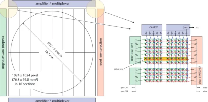
A DEPFET APS matrix has therefore been suggested as a WFI for XEUS [5] by the MPI Halbleiterlabor, where the detector chip is being developed and fabricated. To match the requirements on XEUS the development focuses on a design with 75 × 75 µm
2pixels and an overall active area of 76.8 × 76.8 mm
2corresponding to 1024 × 1024 pixels and a FOV coverage of more than 5 arcmin. For more details see section 4.
The fabrication bases on the technology developed for the XMM pn-CCDs. It consists of several hundreds steps, includ- ing photolithography, ion-implantation, etching, cleaning and thermal treatments. It has been enhanced in many impor- tant details: wafer size increased from 4” to 6”; polysilicon, additional metallization and passivation layers have been introduced. Also the 1999 move of the MPI Halbleiterlabor to a new clean room facility has significantly contributed to an improved device performance.
The DEPFET APS is silicon based and converts incident X-ray photons into signal charges by ionization via photo ef- fect (Compton scattering is negligible in the energy range covered by XEUS). This implies an intrinsic limit for the en- ergy resolution due to statistical fluctuation in the charge creation – the so called Fano noise. Far better (up to a factor of 50) spectral resolution is reached with the cryogenic narrow field imagers (NFIs) on XEUS. The NFIs, however, have a restricted field of view in the order of 0.5 arcmin. Hence, the WFI on XEUS will also be an indispensable pathfinder for the NFI.
2. DETECTOR DETAILS
2.1. DEPFET functional principle
The DEPFET pixel consists of a p-channel field effect transistor realized on high-ohmic, n-type silicon. A schematic view is shown in Figure 1/Left. High quantum efficiency results from the uniform and ultra-thin entrance window [7] as well as from the fully sensitive bulk. This is a benefit from the double-sided processing of the wafer allowing a full de- pletion of the bulk and back illumination. Moreover, an increase of the sensitive thickness from 280 µm (XMM pn- CCDs) to 500 µm further enhances high energy response (see Figure 5 in [8], and [9]).
The back contact is a shallow boron implant forming a pn junction. By applying a negative voltage in the order of 200 V all mobile charges are removed from the bulk and an electric field is created. Signal charges, i.e. electron hole pairs, are separated in that field; holes drift to the p back contact where they are drained off, while electrons are col- lected in a potential minimum below the top surface. That potential minimum – created by high energetic ion implanta- tion – forms the internal gate of the transistor and represents the storage area of the pixel. The transistor current is modulated by the charges in the internal gate and the voltage applied to the external FET gate. For a given external voltage at the FET gate, the current modulation is a precise measure for the amount of charges stored in the internal gate, i.e. in the pixel. A high precision measurement of the charge is possible due to the extremely small capacitance of the internal gate (~ 50 fF) and the resulting conversion factor of at least 200 pA per electron. Since the stored charges are not affected by the transistor current the readout is non-destructive, which turns the DEPFET structure into a mem- ory cell suitable for random access. However, to reset the device the charges must actively be removed. This is done via the n+ clear contact in conjunction with the clear gate by applying appropriate voltage pulses.
Single DEPFET pixels can be arranged in a matrix, the principle is shown in Figure 1/Right by a 3 × 3 pixel subset. In
this case a source follower readout is assumed and the sources are connected column-wise, while all drains are con-
nected to a common voltage. The external gates as well as the reset contacts are interconnect row-wise. Using an indi-
vidual electronic channel to preamplify each column and controlling the row which is active, an unambiguous reading
of each pixel is realized. The row-wise activation is achieved by applying a turn-on voltage to all external FET gates in
one row, while all other rows in the matrix remain turned-off (i.e. their transistor channels are pinched off and no cur-
rent can flow).
row-common gate
row-common clear
common drain common drain
column-common source
internal gate 75 µm
75 µm
Figure 1, Left: Schematic view of a circular DEPFET pixel. X-ray photons enter through the p back contact. Signal charges are stored close to the opposite (top) side. Right: A 3 × 3 pixel circuitry visualizes how DEPFET pixels are in-
terconnected in an APS matrix.
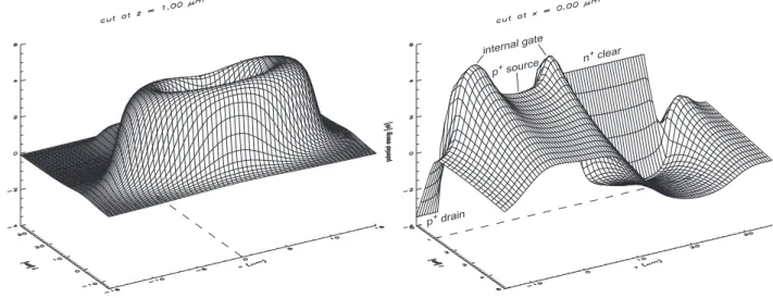
2.2. Simulation of the DEPFET operating states
For design optimization a large number of device simulations have been calculated with the three dimensional Poisson equation solver POSEIDON, developed by A. Castoldi, E. Gatti and P. Rehak within the INFN-RIMAX project [10, 11]. Figure 2 shows a DEPFET structure in signal integration state. The simulated structure has a circular geometry similar to the one in Figure 1, but the central p
+contact is used as the transistor source and the surrounding p
+ring as the drain. Since a three dimensional potential cannot be pictured in print, we show pairs of two dimensional sections.
Their relative locations are indicated: in the right graph a dashed line shows a projection of the left graph’s plane and vice versa.
The left plot of Figure 2 shows the potential in a depth of 1 µ m parallel to the surface (x-y-plane). The center of the pixel, i.e. the center of the circular external FET gate, is located at x = y = 0. The ring shaped potential maximum (minimum for electrons) corresponds to the internal gate, where the signal charges are stored. In the right plot a cut along x = 0 visualizes the internal gate (at y = ±10 µ m) and the n clear contact (between y = 12 µ m and y = 28 µ m).
This section is orthogonal to the surface (y-z-plane). From the right plot also the z-location of the electron potential minimum can be derived: it is at z = 1 µm, where the left plot’s section has been placed.
A simulation of the DEPFET structure during reset is shown in Figure 3. A positive voltage applied to the n clear
contact removes the potential barrier between the internal gate and the n clear contact. Electrons which were stored in
the pixel during integration and readout phase will be completely removed from the internal gate. The removal of all
electrons is essential for the performance of the device, since electrons remaining after reset would contribute with the
square root of their number to the noise.
p+ source
n+ clear internal gate
p+ drain
Figure 2: Simulation of the potential in a DEPFET pixel structure during signal integration calculated in three dimen- sions by the Poisson equation solver POSEIDON. Left: potential parallel to the detector surface in a depth of 1 µ m.
Right: potential perpendicular to the surface.
p+ source
n+ clear
internal gate
p+ drain
clear gate
Figure 3: POSEIDON simulation of a DEPFET pixel structure during reset. Again, the left and right plots are different sections through a potential calculated in three dimensions.
2.3. APS system design
As already shown in Figure 1/Right the pixel outputs (sources) are connected column-wise. Each column of outputs is further processed by one channel of a multiplexing preamplifier chip. Figure 4 outlines a complete system including an APS device, control and readout electronics. Every row of pixels is interconnected via their external gate and n clear contacts. Readout of the matrix is realized row by row, i.e. by turning on the transistor currents via the common exter- nal gate connection.
For redundancy and performance reasons the 1024 × 1024 pixel matrix is subdivided in 16 units of 128 × 512 pixels,
each read out by a 128-channel, multiplexing preamplifier chip (CAMEX). Row-wise selection for readout and reset is
realized by switcher chips on the left and right sides of the APS. Since the upper and lower 8 subunits are independent
two rows (2 × 1024 pixels) can be processed simultaneously.
CAMEX
FOV = 5 arc
min 72.7 m
m
gateSWITCHER
MUX ADC
gate OFF clear OFF
gate ON clear ON
1024 x 1024 pixel (76.8 x 76.8 mm²) in 16 sections
amplifier / multiplexer
readout row selection
amplifier / multiplexer
reset row selection
clearSWITCHERactive rowFigure 4: The APS system concept includes readout and steering electronics. The gate SWITCHER chips selectively activate single rows of 1024 DEPFET pixels for readout. The selection of a row to be reset is done by the clear SWITCHERs. 16 multiplexing preamplifier chips (CAMEX) receive the signals from the column-wise connected
DEPFET sources.
2.3.1. CAMEX analog amplifier/multiplexer
A new version of the XMM-proven CAMEX chip [12] is being adapted to the requirements of the pixel sensor readout.
Now 128 input channels (64 on XMM) are multiplexed into one output. The input stage still uses multi-correlated sam- pling for noise filtering. The technical innovations include the modification of the CAMEX integrated current source to match the DEPFET amplifier, the integration of a shift register for the storage of the timing sequence, an enhanced out- put buffer which is able to run at a frequency of 16 MHz, and a new approach towards the problem of common-mode fluctuations, which is based on the reading of ‘empty’ (i.e. non-connected) channels. Also different filtering techniques are studied and the layout has been modified to fit to the 75 µ m pitch of the APS output contacts.
2.3.2. Readout and reset select SWITCHER
For the row by row access the APS system is equipped with the so-called SWITCHER chips. The current version can address 64 rows and has two voltage outputs per row. Two outputs are needed to supply individual pulse levels for the clear gate and n clear during reset. The timing of the voltage output is controlled by a 256 x 4 Bit RAM sequencer. This allows selecting from four input voltages and switching them to the two currently active outputs. It is fabricated in a high-voltage CMOS technology (AMS0.8µ m “HV”, see [13]) allowing a range from +2 V to +20 V for the n clear and clear gate and from -15 V to -5 V for the external gate.
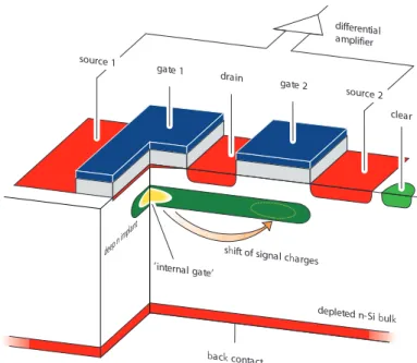
2.4. Repetitive non-destructive readout (RNDR)
By making use of the non-destructive character of the readout it is possible to further decrease the readout noise
contribution. In Figure 5 the principle is shown: two adjacent DEPFET devices are able to transfer the signal charges
from one floating gate amplifier to the neighboring one, reading the same signal charges several times. The read noise is
reduced by the square root of n, where n is the number of readings.
back contact deep
n implant
depleted n-Si bulk
’internal gate’ shift of signal charges
differential amplifier gate 1
gate 2 drain
clear source 1
source 2