IMAGING SPECTROMETERS FOR FUTURE X–RAY MISSIONS
L. Str¨ uder
1 •, G. Hasinger
1, J. Kollmer
1 •, N. Krause
1 •, N. Meidinger
1 •, J. Tr¨ umper
1, R. Hartmann
2 •, P. Holl
2 •, P. Lechner
2 •, H. Soltau
2 •, P. Klein
3 •, G. Lutz
3 •,
R.H. Richter
3 •, P. Fischer
4, N. Wermes
4and W. Buttler
51
Max-Planck-Institut f¨ ur extraterrestrische Physik Gießenbachstr., D-85740 Garching, Germany
2
KETEK GmbH
Am Isarbach 30, D - 85764 Oberschleißheim, Germany
3
Max-Planck-Institut f¨ ur Physik
F¨ ohringer Ring 6, D - 80805 M¨ unchen, Germany
4
Universit¨ at Bonn, Physikalisches Institut Nussallee 12, D - 53115 Bonn, Germany
5
Ingenieurb¨ uro W. Buttler
Uberruhrstr. 476, D - 45277 Essen, Germany ¨
•
also at MPI-Halbleiterlabor, Otto-Hahn-Ring 6, D-81739 M¨ unchen, Germany
Abstract
Based on the operational experience with the EPIC pn-CCD system on board of XMM-Newton [1], new imaging X-ray spectroscopic detector systems for future X-ray missions will be introduced in terms of energy, position and time resolving detectors.
As the readout speed requirement in the case of single photon counting detectors increases drastically with the collecting area and improved angular resolution, but noise figures have to be on the lowest possible level, new detector schemes must be developed: Active pixel sensors (APS) for X-ray detection have the capability to randomly select areas of interest and to operate at noise levels below 1 electron (rms). About 1000 frames per second can be read out with a relatively low level of electric power with the proposed DEPFET arrays.
One prominent candidate for the use of an APS is ESA’s XEUS – the X-ray Evolving Universe
Spectroscopy mission. It represents a potential follow-on mission to the cornerstone XMM-Newton,
currently in orbit. The XEUS mission is considered as part of ESA’s Horizon 2000
+program within
the context of the International Space Station (ISS).
1 Introduction
Future X-ray missions will require focal plane instruments with pixel sizes in the order of 75 µ m and with a position resolution in the 50 µ m range, faster readout because of the highly increased effective telescope area, and improved quantum efficiency at the high and low energy end. In addition operation should be possible at higher temperatures and the optical light should be blocked at the camera level to avoid large area fragile structures in front of the radiation entrance window.
To face this situation we pursue two options: (1) The continuous improvement of the pn-CCD technology and operation, and (2) the development of a new detector-amplifier structure (DEPFET) operating as an active pixel sensor [2]. Recent results will be presented.
The frame store pn-CCD development is described in detail in the paper [3]. Both detector systems, the CCD as well as the APS may cover the radiation entrance side with a thin aluminum layer acting as a light blocking filter in the visible. A 100˚ A thick monolythically grown Al layer reduces the optical throughput by a factor of 5 × 10
6, but also lowers the quantum efficiency at e.g. C
Kfrom 90% without filter to 40% with the Al filter. But large area fragile thin filters can be avoided (see ref. [3]).
In addition both detector systems can be operated with a spectroscopic high speed channel, being able to process 10
7X-rays per second within an active area of 10 to 20 mm
2based on an silicon drift detector.
2 Active Pixel Sensors
Several limitations of CCD type detectors operated as a single photon counter, can be overcome by pixel detectors, where every pixel has its own amplifier. A long charge transfer through the device is not needed any more and every pixel could be x-y-addressable offering an observation adapted readout mode. In addition, the signal charge can be read out several times, reducing the electronic noise with the square root of the number of readings.
2.1 The DEPFET Principle
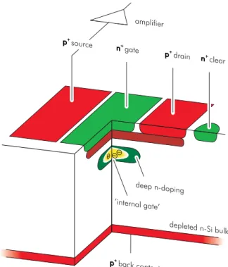
The DEPFET is a p-channel field effect transistor on high resistivity n-type bulk [5]. The transistor may be either a JFET, or a MOSFET of enhancement and depletion type. The bulk is completely depleted by the reverse biased backside diode, thus creating a potential minimum for electrons close to the surface. An additional buried n-doped channel underneath the transistor gate enhances the potential minumum for electrons and thus confines them to the region below the FET channel (see Fig.1). Each electron released in the depleted volume below the transistor by absorption of ionizing radiation or by thermal generation will drift to the potential minimum, called ‘internal gate’, and enhance the transistor current by inducing an additional positive charge inside the FET channel.
Thus, the DEPFETs current is a function of the amount of charge in the potential minimum, and its
measurement yields information about the energy absorbed in the depleted volume. One electron in
the ‘internal gate’ typically increases the transistor current by 0.5 nA. Depending on leakage current
p+back contact
depleted n-Si bulk
’internal gate’
deep n-doping amplifier
n+gate
p+drain n+clear p+source
Figure 1: Cross section of a DEPFET. Signal electrons stored in the internal gate steer the current of the p-channel JFET. The n
+clear removes the charges under the p-channel after the first amplification is completed.
and signal rate the internal gate has to be reset periodically by applying a positive voltage to an adjacent n
+-doped ‘clear’ contact to remove the stored electrons.
Charge collection in the internal gate functions equally well, when the transistor current is turned off.
Therefore it is also possible to collect the signal charge in “off” state condition, measure the current after turning the transistor on with the external gate and compare this current with that obtained after emptying the internal gate with the help of the n
+clear contact. As only the DEPFET pixels are powered which are read out, the total power dissipation can be reduced by a factor of 1,000 for the whole focal plane. This leads to a total power requirement for the focal plane of approximately 15 W including signal processing and analog-to-digital conversion.
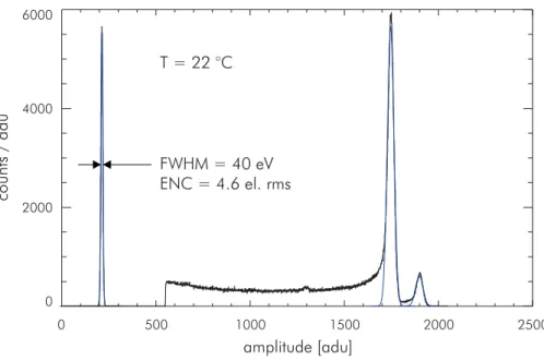
Unlike a conventional detector-preamplifier system the DEPFET is free of interconnection strays capacitances. The noise characteristics of single DEPFET devices have been evaluated by spectroscopic measurements. From the width of the noise peak an equivalent noise charge (ENC) of 4.6 electrons (rms) at room temperature and 3.6 electrons (rms) at – 60
◦C has been deduced (see Figs. 2 and 3).
The measurement of 4.6 electrons (rms) is to our knowledge the best spectroscopic measurement at room temperature ever made with silicon.
The remomal of charges (from signal and leakage current) can be done in an elegant way: A small
ohmic n
+contact, the clear contact, to be seen on the left side of Fig. 1, can be electronically hidden
amplitude [adu]
FWHM = 40 eV ENC = 4.6 el. rms
counts / adu
0 2000 4000 6000
500 1000 1500 2000 2500
0
T = 22 °C
Figure 2: Measurment of the Mn K
αand Mn K
βspectrum of an
55Fe source at room temperature with a single DEPFET structure. The position of noise peak indicates zero of the energy scale, Mn K
αis at 5.898 keV, Mn K
βat 6.49 keV. The continuous hits from ADC count 550 (trigger threshold) to 1,700 is due to split events at the border of the pixel.
amplitude [adu]
FWHM = 32 eV ENC = 3.6 el. rms
counts / adu
0 1·105
4
4
4
4
8·10
6·10
4·10
2·10
500 1000 1500 2000 2500
0
T = -60 °C
Figure 3: Measurment of the Mn K
αand Mn K
βspectrum of an
55Fe source at – 60
◦C. The Si K
αline at 1.74 keV and the escape peak at 4.15 keV is clearly to be seen. The ENC of this measurement
is 3.6 electrons (rms)
radius [µm]
depth[µm]
10 0
5
15
20
0 5 10 15 20
source gate clear gate clear
radius [µm]
depth[µm]
10 0
5
15
20
0 5 10 15 20
source gate clear gate clear
radius [µm]
depth[µm]
10 0
5
15
20
0 5 10 15 20
source gate clear gate clear
electron density [1/cm³]
radius[µm]
0
5 10
15 20 0
5 10
15 20 10
10 10 10 10
0 5 10 15 20
depth [µm]
source gate
cleargate clear
electron density [1/cm³]
radius[µm]
0
5 10
15 20 0
5 10
15 20 10
10 10 10 10
0 5 10 15 20
depth [µm]
source gate
cleargate clear
electron density [1/cm³]
radius[µm]
0
5 10
15 20 0
5 10
15 20 10
10 10 10 10
0 5 10 15 20
depth [µm]
source gate
cleargate clear
filled internal gate
clear pulse
empty internal gate
Figure 4: Simulation of the charge integration and clear process in DEPFET type detector-amplifier
structures. Upper plots: electron density and electric potential during the signal integration, center
plot: during the clear process and lower plot: after clearing of the pixel.
in the substrate: It remains attractive for electrons during the clear process, but during the signal integration time, when the transistor is in “off” state, its capability to attract electrons can be com- pletely suppressed; no signal electron can reach the clear contact The intergation and clear process is shown in the device simulation of Fig. 4. In the upper plot the electron density distribution is schown as well as the electric potential during the signal integration phase. Upon request, a positive pulse is applied to the n
+clear contact, removing all electrons from the internal gate (center plots).
Immediately alter the clear process no electron (less than 10
−3electrons per pixel) are left under the transistor channel (lower plot).
2.2 DEPFET arrays as Active Pixel Sensors
The matrix-like arrangement of DEPFETs with a single common back contact results in a back illuminated APS system with 100% fill factor, i.e. no signal charge is lost between the pixel boundaries or in the electronics implemented in the pixel area. Therefore this concept is actually the only APS suited for spectroscopic X-ray measurements. The depletion depth at present is 300 µ m . In the upcoming fabrications on 6 inch wafers with 500 µ m sensitive volume the quantum efficiencies will be above 95% at 10 keV and still 40% at 20 keV. In the low energy part of the spectrum the thin entrance window technology guarantees a quantum efficiency above 90% for energies around 300 eV, however, without the Al light filter.
All DEPFETs in the pixel sensor have a common drain contact, while the gates and clear contacts are connected row-wise and the source contacts, i.e. the signal lines are connected within each column as can be seen in Fig.5. In normal operation the transistors of one row after the other are turned on, read and cleared by CMOS control chips. While the DEPFETs of the active row are read in parallel by a multi-channel CMOS preamplifier/multiplexer of the CAMEX type [6], the rest of the pixels is turned off, but still capable to collect signal charge, thus keeping dead time short and power consumption low. The read time for one row is of the order of a few µ sec. That keeps the so called out-of-time events, i.e. events hitting the DEPFET during readout well below 0.5%. Besides the usual full frame readout mode the random accessibility of the pixels allows for any kind of windowing or mixed mode, in which only a selected region of interest is read with higher speed, while the remaining area is read at a lower rate.
On our way to the proposed focal plane detector for XEUS smaller devices have been produced
and tested together with the CMOS control electronics. First X-ray images have been recorded
with reasonable quality proving the functional principles of the whole sensor concept [7]. In this first
system several technological problems have limited the resolution: (a) inhomogeneous implants leading
to a spatial variation of DEPFET currents; (b) large resistance of inter-chip connections due to the
availability of only one interconnection metal layer at that time and (c) a complete clear of the signal
charges was not possible due to limitations in the CMOS circuits. The clear contact was too attractive
for signal charges during readout. A new version of DEPFETs and CMOS electronics which avoids
the above limitations is in production.
CAMEX amplifier
RESET row select
READOUT row select
MUX ADC
gate
clear
internal gate
active row common
drain
source
gate ON clear ON
gate OFF clear OFF
Figure 5: Concept of a DEPFET active Pixel sensor readout, including the control CMOS electronics
‘readout row select’ and the ‘reset row select’.
2.3 The non-destructive readout of DEPFETs
In a DEPFET the signal charges are stricly confined in a potential well below a single transistor. The information, i.e. the number of charges in the internal gate, is conserved during the readout so that multiple reading of the same signal charges with subsequent averaging is possible. Repetitive readout results in a serial noise reduction by √
n , with n the number of read cycles, allowing spectroscopy
measurements with a noise contribution (ENC) of a single electron. The technique of repetitive non-
destructive readout is best realized by the combination of two neighbouring DEPFETs within one
pixel (see Fig. 6). The signal charge can be shifted repeatedly between two neighbouring gates. That
way one of the DEPFETs reads the signal while the other one reads the reference value (baseline)
of the empty internal gate. Devices of that type are currently under test. In dedicated areas the
repetitive reading may be applied, while the rest of the sensor can be read out conventionally (see
chapter 2.2). This offers a large variety of observation adapted operating modes. Therefore, compared
to CCD type operation, windowing modes do no longer lead to a loss of sensitive area in order to gain
readout speed.
deep n implant
back contact
depleted n-Si bulk
’internal gate’
clear of signalcharges differential amplifier
gate 1
gate 2 drain
clear source 1
source 2
back contact deep
n implant
depleted n-Si bulk
’internal gate’
shift of signalcharges differential amplifier
gate 1
gate 2 drain
clear source 1
source 2