Nuclear Instruments and Methods in Physics Research A 509 (2003) 302–314
X-ray imaging spectrometers in present and future satellite missions
P. Lechner
a,b,*, R. Hartmann
a,b, P. Holl
a,b, G. Lutz
b,c, N. Meidinger
b,d, R.H. Richter
b,c, H. Soltau
a,b, L. Str uder .
b,daKETEK GmbH PNSensor GmbH, Munchen, Germany.
bMPI Halbleiterlabor, Otto-Hahn-Ring 6, D-81739 Munchen, Germany.
cMax-Planck-Institut fur Physik, M. unchen, Germany.
dMax-Planck-Institut fur extraterrestrische Physik, Garching, Germany.
Abstract
Observations in X-ray astronomy require imaging spectroscopy detectors with high-energy resolution, high quantum efficiency, two-dimensional position resolution, large sensitive area, low power consumption, and fast readout. This paper gives a review of the functional principle and performance of fully depleted pn-CCDs and DEPFET based Active Pixel Sensors, both developed at the semiconductor laboratory in Munich, Germany. While pn-CCDs have proved their quality and reliability onboard of the European XMM-Newton satellite in the last 3 years, the Active Pixel Sensor is a promising candidate for the Wide Field Imager of the future XEUS mission.
r 2003 Elsevier B.V. All rights reserved.
Keywords: X-ray imaging; X-ray detector; X-ray CCD; pn-CCD; Active pixel sensor
1. Introduction 1.1. X-ray astronomy
X-ray astronomy is a relatively young branch of astrophysics with first observations only made in the 1960s [1]. Because the Earth’s atmosphere is completely opaque to X-rays, i.e. photons in the energy range from 50 eV to 500 keV, observations depend on satellite-based instruments. In space X-rays are either generated thermally by hot objects with temperatures above 10
6K, e.g. in the
shock wave of a supernova explosion, or emitted by energetic non-thermal processes, e.g. synchro- tron radiation of charged particles accelerated by compact massive objects as black holes. The scientific assessment of an X-ray source requires knowledge about both the energy spectrum and the spatial distribution of the emission. The astrophysical demands have therefore driven the development of both X-ray imaging optics and high-resolution energy-dispersive pixellated detec- tor systems during the past decades.
1.2. X-ray optics
Due to the physics of their interaction with matter, i.e. absorption at normal incidence, X-ray
*Corresponding author. Tel.: +49-89-83940051; fax: +49- 89-83940011.
E-mail address:peter.lechner@hll.mpg.de (P. Lechner).
0168-9002/03/$ - see front matterr2003 Elsevier B.V. All rights reserved.
doi:10.1016/S0168-9002(03)01642-5
photons cannot be focussed by diffraction like longer wavelengths. X-ray telescopes are therefore equipped with focussing mirror systems based on grazing incidence total reflection. The two large operational observatories, NASA’s Chandra [2]
and ESA’s XMM-Newton [3], both carry X-ray optics of the Wolter-type I, i.e. mirrors with combined parabolic and hyperbolic surfaces [4,5].
The effective area of the Wolter-I telescope is increased by confocal nesting of a large number of individual mirror shells. For instance, the three telescopes onboard XMM-Newton consist of 58 shells. At increasing X-ray energy the effective mirror area decreases with the cut-off angle for total reflection. The collecting area of one XMM- Newton mirror system, the largest X-ray telescope ever built, is about 1200 cm
2at 1 keV and about 150 cm
2at 10 keV. The use of mirror optics is therefore constrained to a maximum energy which is defined by the focal length of the telescope.
XMM-Newton and Chandra with focal lengths of 7.5 and 10 m have a high-energy limit of about 10 keV. For harder X-rays, different imaging methods like collimators or coded masks have to be used.
The angular resolution of an X-ray telescope is specified in terms of Half Energy Width (HEW) which is the diameter of a circle that contains 50%
of the photons emitted by a point source. The XMM-Newton telescopes have an HEW of about 15 arcsec translating to a spot size of 500 mm in the focal plane.
1.3. Imaging spectroscopy detectors
The required performance of the focal plane detector is obvious: high-energy resolution to resolve the characteristic X-ray emission lines even of light elements, high quantum efficiency, two- dimensional position resolution compatible with the telescope’s HEW, large sensitive area to cover the full field of view, and fast readout to avoid event pileup. There is a variety of X-ray detector principles and materials that are superior in one of the above categories: position sensitive propor- tional gas counters with sensitive areas of several 100 cm
2, scintillators and high-Z compound semi- conductors with high detection efficiency up to
highest X-ray energies, avalanche photodiodes with time resolution in the pico-second range, cryogenic detectors like bolometers or supercon- ducting tunnel junctions with energy resolution in the order of 1 eV.Nevertheless, up to now the broad band (set/spectrum?) of desired properties has only been unified by state-of-the-art Charge Coupled Devices (CCDs) based on silicon and with integrated readout electronics, while the Active Pixel Sensor (APS) with one amplifying element per picture cell is a promising option for the future.
The following sections highlight the develop- ment of pn-CCDs and Active Pixel Sensors for the missions XMM-Newton XEUS at the semicon- ductor laboratory of the Max-Planck-Institutes for physics and for extraterrestrial physics (MPI Halbleiterlabor, MPI-HLL) in Munich, Germany.
2. Fully depleted backside illuminated pn-CCDs for XMM-Newton
The satellite XMM-Newton (X-ray Multi Mir- ror mission) carries three identical Wolter-I mirror systems. One telescope has a pn-CCD in the focal plane, while both other telescopes are equipped with an MOS-CCD array [6] and an additional reflecting grating spectrometer [7].
The development of the pn-CCDs started in 1985. In the following years the basic concept was simulated, modified and designed in detail [8,9]. N- channel JFET electronics were integrated in 1992 [10–12] and the first full working devices with a sensitive area of 3 1 cm
2were produced in 1993 [13,14]. The flight type monolithic large area detectors with an area of 6 6 cm
2were produced from 1995 to 1997, with a sufficiently high yield to equip the X-ray satellite mission XMM-Newton [15–19] with a defect free focal plane imager. In this overview the basic detector features will be shown as well as the measured performance in space.
2.1. The pn-CCD concept
Conceptually the pn-CCD is the adaptation of
clocked charge transfer parallel to the detector
surface to the principle of sideward depletion [20].
A double sided polished high resistivity (10
12cm
3) n-type silicon wafer is covered with rectifying p
+boron implants on both surfaces.
The p
+junctions are reverse biased with respect to a small sized ohmic bulk contact, the charge collecting n
+doped anode, so that the wafer volume is fully depleted and a potential minimum for electrons exists within the wafer. To obtain a pronounced potential minimum in a defined depth of about 10 mm an additional higher n-doped (10
14cm
3) 12 mm thick epitaxial layer is deposited on the upper side and asymmetric voltages are applied on both surfaces ( 15 V to 20 V on the upper side, 160 V on the backside, Fig. 1).
To realize a CCD-type detector, the upper p
+implant is divided in p
+strips or shift registers as shown in Fig. 1 with three strips comprising one pixel. A periodic modulation of the register voltages F
1, F
2, F
3generates potential wells in the direction perpendicular to the strips, while in the lateral direction the pixel is confined by deep channel stop and channel guide implants. Elec- trons released by the absorption of ionizing radiation within the depleted volume drift to the local potential minima of the pixels and are stored at the projected position of their generation, while the holes move to the negative biased p
+contacts.
Clocking the voltages F
1, F
2, F
3in a defined way the stored signal electrons are transferred to the readout node. The charge transfer is illustrated by the simulated pn-CCD potential (Figs. 2a–c)
obtained by the two-dimensional device simulator TeSCA [22].
One pn-CCD unit with a sensitive area of 3 1 cm
2consists of 200 rows in readout direction and 64 individual transfer channels. The 150 150 mm
2pixel size was chosen on one side to be well below the telescope’s 15 arcsec (HEW) resolution and on the other side as large as possible to avoid unnecessary oversampling and to keep the readout time short. Each transfer channel is terminated by an on-chip preamplifier of the single-sided N-JFET type [10–12]. The preamplifier signals are transferred to CAMEX amplifier/multiplexer chips in VLSI JFET-CMOS technology [21,23]. For the XMM-Newton focal plane detector, 12 of these units with 200 768 pixels and a sensitive area of 6 6 cm
2are integrated monolithically in a gapless array on a 4-in. wafer (Fig. 3).
Compared to standard CCDs the pn-concept has a number of intrinsic advantages:
*
flexible pixel size varying from 30 to 300 mm, allowing optimum adjustment of the pixel size to the resolution of the X-ray optics;
*
deep transfer of signal charges, high transfer efficiency;
*
full depletion of the detector bulk, high quantum efficiency for harder X-rays;
*
backside illumination through homogeneous, thin, p
+implanted entrance window, high quantum efficiency for soft X-rays;
*
fast readout by parallel signal processing and large pixel size.
2.2. Detector performance
Before satellite integration and launch the pn- CCD had to undergo a full device characterization in laboratory environment. The following list gives a summary of the relevant measured detector parameters.
*
The best value for the readout noise of the on- chip electronics expressed in Equivalent Noise Charges (ENC) is 3 el. rms at 150 K. Typical values scatter around 4–5 el. rms including thermal and low-frequency noise of the on-chip FET and parallel noise due to leakage current.
Fig. 1. Schematic cross-section through the pn-CCD along a transfer channel. The device is back illuminated and fully depleted over 300mm.
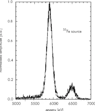
The corresponding line width (FWHM) of the Mn–Ka line at 5.9 keV is 120 eV to 126 eV (Fig. 4). The XMM-Newton flight camera was operated at 90
C on ground during calibra- tion with a resolution of about 145 eV (FWHM) over the entire area of 36 cm
2. The main effect on the degradation of energy resolution was the reduction of the charge transfer efficiency (CTE) at warmer temperatures.
*
The charge transfer properties of the pn-CCDs are in the order of a few percent signal loss from the last to the first pixel over 200 pixels or a distance of 3 cm. As the charge transfer losses describe the position dependent energy resolu- tion, it is one of the key parameters for the
spectroscopic performance, especially after ra- diation damage may have occurred.
*
The equivalent fluence of 10 MeV protons over the expected life time of XMM-Newton is 4 10
8p/cm
2. Fig. 5 shows the results of the irradiation tests with 10 MeV protons: the expected decrease of energy resolution over the 10 year dose is from 145 to 158 eV at an operating temperature of 100
C.
*
The quantum efficiency was measured in single photon counting mode with respect to a calibrated solid state detector. Fig. 6 shows measurements from the synchrotron radiation facilities in BESSY Berlin and in Orsay. The quantum efficiency is well above 90% in the
Fig. 2. Electron potential of a pn-CCD simulated by the two-dimensional device simulator TeSCA [22]. The signal charges are:
(a) stored under the registerF3only, (b) then share a larger volume under the registersF2andF3, and (c) are stored under the register F2only. For clarity the depleted bulk is only shown up to the depth of 40mm.
whole energy range from 300 eV to 10 keV. On the low energy side the quantum efficiency reflects the quality of the entrance window, while on the high-energy end it is limited by the wafer thickness of 280 mm. At 525 eV a 5% dip can be seen from the absorption at the oxygen edge in a thin SiO
2layer covering the entrance
window. The same happens at the Si-K edge at 1840 eV showing the fine structure of a typical XAFS spectrum (see inset of Fig. 6). For all energies the quantum efficiency is represented by a model using the photo absorption coeffi- cients from the atomic data tables.
*
Due to the large pixel size and the parallel processing of the channels the full frame of a 3 1 cm
2pn-CCD unit is read out in 5 ms.
Compared to a conventional CCD with serial readout this is faster by two orders of magni- tude. The readout electronics of the pn-CCD system is described in Refs. [21,23]. A charge sensing amplifier followed by a multi-corre- lated sampling stage, multiplexer and output amplifier (CAMEX64B JFET/CMOS chip) guide the pn-CCD pixel content as a voltage signal to a 10 MHz 12-bit flash ADC system.
The whole system, i.e. CCD and CAMEX64B
Fig. 4. Spectrum of a55Fe source with the Mn-Kaand Mn-Kb lines at 5.9 and 6.5 keV recorded with a pn-CCD. The measured energy resolution is 130 eV (FWHM) at an operating tempera- ture of 120C.
Fig. 5. 55Fe energy spectrum after different proton fluences of 0 p/cm2 (dotted line), 4108p/cm2 (solid line), which is the expected fluence over a lifetime of 10 years in space. The spectra have been normalised with respect to the amplitude of the 5.9 keV line. The increase of the measured FWHM of the Mn- Ka line from 152 to 173 eV is tolerable for the onboard operation.
Fig. 3. The focal plane of the pn-CCD camera on XMM and ABRIXAS consist of 12 independent, monolithically integrated pn-CCDs with a total area of 66 cm2. In total 768 on-chip amplifiers process the signals and transfer them to a VLSI JFET-CMOS amplifier array. Twelve output nodes of the CAMEXarrays are fed into 4 ADCs, i.e. one ADC per quadrant.
amplifier array dissipate a power of 0.7 W for the entire camera (12 64=768 readout chan- nels), a value which is tolerable for the XMM- Newton satellite mission.
2.3. Operation in orbit
XMM-Newton was launched on December, 10th in 1999 from Kourou in French-Guyana.
The satellite is placed in a highly eccentric 48-h elliptical orbit around the earth. Inclined at 40
with a southern apogee at 114,000 km, the perigee altitude is 7000 km. Astronomers have the ob- servatory at their disposal for about 40 h per revolution. In the remaining time, while passing the Earth’s radiation belt, the telescopes are protected by cover shields. Commissioning of the scientific payload was completed and the acquisi-
tion of scientific data started in the middle of March 2000.
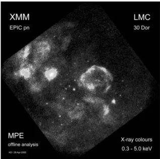
After the switch-on of the pn–CCD camera the detector performance known from calibration on ground could be reproduced. During the first 500 revolutions (status of September 2002) all system parameters stayed stable and more than 1000 scientific observations have been made using the pn–CCD camera. The first light image of the large Magellanic cloud (Fig. 7) summarizes qualitatively the in-orbit performance of the system.
In revolution No. 156 the sudden appearance of about 35 permanent ‘bright’ pixels with a drastic increase of locally generated leakage current spread over the detector area was observed. As there is no explanation by detector inherent phenomena the effect is attributed to the impact of a micro-meteorite reflected off the mirror
Fig. 6. Quantum efficiency of the pn-CCD as a function of the incident photon energy. The energy scale ranges from 150 eV to 30 keV.The theoretical curve perfectly fits the measured values. The solid line represents a 300mm thick sensitive volume, the dotted line 500mm. The insert shows the X-ray absorption fine structure (XAFS) of the Si-K edge at 1838 eV.
surface [24]. It was reproduced on ground with the use of a dust particle accelerator [25].
3. DEPFET based active pixel sensors for XEUS 3.1. The XEUS mission
The X-ray Evolving Universe Spectroscopy (XEUS) mission is a potential follow-on mission to the XMM-Newton satellite and currently under study within the European Space Agency’s (ESA) Horizon 2000+ program [26].
The aim of XEUS is to operate a permanent satellite observatory for the X-ray energy band from 100 eV to 30 keV with a telescope aperture equivalent to the largest ground based optical
telescopes, i.e. in the order of 10 m
2. XEUS will be the first instrument to perform detailed imaging spectroscopic studies of some of the unresolved issues of high-energy astrophysics concerning the early stage of the universe. Among the scientific goals are the study of first massive black holes, the formation of first gravitationally bound galaxy groups and their clustering evolution, and the evolution of chemical element synthesis.
The initial mission configuration will consist of a mirror spacecraft (MSC) with an effective area of 6 m
2at 1 keV and a separate detector spacecraft (DSC). The two spacecrafts are aligned by active control at a focal length of 50 m with a relative accuracy of 1 mm
3. After several years of opera- tion XEUS will dock to the International Space Station ISS where the MSC will be upgraded to an effective area of 30 m
2at 1 keV by the robotic mounting of additional mirror segments. A new detector spacecraft with advanced sensor technol- ogy will then replace the DSC.
The launch of XEUS will be presumably in 2012. With the potentialities of the ISS for mirror extension, and with the option of detector substitution the mission lifetime may be well over a quarter of a century.
The XEUS focal plane instrumentation will consist of two Narrow Field Imagers (NFIs) and a Wide Field Imager (WFI). The NFIs will be based on cryogenic imaging spectrometers like super- conducting tunnel junctions and/or transition edge sensors and cover a field of view (FOV) of 1 arcmin, i.e. about 1.5 1.5 cm
2at 50 m focal length. With their energy resolution of 1–10 eV FWHM over the full energy range from 100 eV to 30 keV the NFIs will be able to resolve the fine structure in the X-ray emission of differently ionized atoms.
3.2. The XEUS wide field imager
The WFI on XEUS will work mainly as a pathfinder for the NFIs. It will cover a 5 arcmin FOV, translating into a total detector area of 7.5 7.5 cm
2. To match the spatial resolution of 2 arcsec (HEW) of the telescope the pixel size has to be smaller than 100 100 mm
2. The WFI’s envisaged energy resolution is of 50 eV FWHM
Fig. 7. First Light Image of the pn-CCD camera: the Large Magellanic Cloud in X-ray colours. The field of view of 30 arcmin corresponds approximately to our perception of the size of the moon. The image shows the area of 30 Doradus a supernova remnant as an extended source of X-rays. The
‘north-east’ of 30 Doradus shows an emission of X-rays up to 5 keV (blue), while the ‘south-west’ rim appears much softer in X-rays (yellow and red). The supernova 1987A is the bright source ‘south west’ of 30 Doradus. About 40 new X-ray objects have been found in this exposure. The exposure time was about 10 h. Of course, all scientific information about the X-ray sources, such as energy spectra, light curves, etc. are stored as data but not included in the coloured image representation.
at the C–K line (272 eV) and 125 eV FWHM at the Mn–Ka line (5.9 keV).
Compared to the current X-ray satellite mis- sions XMM-Newton and Chandra, the XEUS telescope will bring an enormous increase in sampling area. The throughput will grow by a factor of 25 in the initial XEUS configuration with respect to XMM-Newton, and by a factor of 100 after the mirror upgrade. Developing a detector for the WFI count rate capability has to be one of the major concerns.
CCDs have been the dominant image sensor technology during the past decades for visible light as well as for X-rays. However, the CCD concept has fundamental handicaps inherent to the need of a close-to-perfect charge transfer over macroscopic distances inside the semiconductor bulk [27]: (i) The required high charge transfer efficiency depends on the quality of the bulk material and may deteriorate by radiation damage during the CCD’s lifetime [28]. (ii) The relatively slow transfer process limits the readout rate. (iii) The access to the individual pixel contents is strictly sequential.
(iv) Out-of-time events, i.e. photons hitting the CCD during the charge transfer cycle, appear at an erroneous position in the image.
We therefore started—similar to the develop- ment of the pn-CCDs—to adapt the concept of the Active Pixel Sensor (APS), which has gained a considerable share in the market of optical digital photography, to the principle of sideward deple- tion [20] in order to meet the requirements of X-ray imaging spectroscopy. An APS is defined as a two-dimensional structured detector array with an amplifying element in each pixel. As integrated amplifier the DEPFET (DEpleted P-channel Field Effect Transistor) is introduced in the next section.
3.3. The DEPFET concept
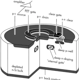
The DEPFET was introduced in 1987 [29, 30]. It consists of a p-channel field effect transistor on a high resistivity n-type silicon bulk. The transistor may be either a JFET, or a MOSFET of enhancement or depletion type. The bulk is completely depleted by the reverse biased backside diode thus creating a potential minimum for electrons close to the surface. An additional deep
n-doped region enhances the depth of the potential minimum and confines it in the lateral direction to the extent of the FET channel (Fig. 8).
Each electron released in the depleted volume by thermal generation or by the absorption of ionizing radiation will drift to the potential minimum and enhance the transistor current by inducing an additional positive image charge inside the FET channel. Thus the DEPFET’s current is a function of the amount of charges in the potential minimum, and its measurement yields information about the energy absorbed in the depleted volume. To express the current steering function of the stored electrons the potential minimum is called ‘internal gate’.
The internal gate exists, i.e. electrons can be collected stored in it, regardless of a current flowing in the channel of the DEPFET or not.
The transistor current may be turned off during integration and only switched on via the external gate for the signal readout, thus minimizing power consumption. The internal gate has a measured sensitivity of 200 pA per electron [31].
Fig. 8. DEPFET in circular geometry. Electrons generated by the absorption of ionizing radiation will drift to the potential minimum of the ‘internal gate’ and enhance the transistor current by inducing an additional positive image charge inside the FET channel. Applying a positive voltage pulse to the clear contact and to the MOS clear gate resets the device.
Its geometric size and doping concentration are dimensioned to store up to a total of 10
5electrons.
Unlike a conventional detector–preamplifier sys- tem, the DEPFET is free of interconnection stray capacitance and the overall capacitance is mini- mized. Depending on leakage current and signal rate the device must be reset periodically by emptying the internal gate. This is done by applying a positive voltage pulse to an adjacent n
+doped ‘clear’ contact acting as drain for electrons. The clear contact is separated from the detector bulk by a deep p-implanted well (Fig. 8).
The usual DEPFET operation follows the sequence: (i) integration of signal charges, (ii) switch-on of the DEPFET current by the external gate, (iii) signal readout with filled internal gate, (iv) reset by the clear contact, (v) baseline readout with empty internal gate, (vi) switch-off of the DEPFET current. This readout scheme requires a reproducible baseline, and the complete removal of the signal electrons from the internal gate is mandatory. Otherwise, the undefined number of remaining electrons in the internal gate would cause the problem of kTC- or reset noise [32]. For an efficient reset an additional MOS ‘clear gate’ is placed between the external gate and the clear contact. During signal integration and readout, the clear gate is biased to a negative voltage to define a potential well that restricts electrons to the
internal gate. For the reset both clear contact and clear gate are set to a positive voltage.
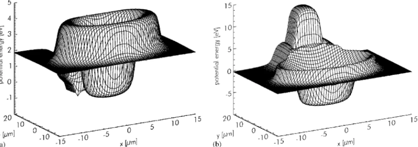
The different DEPFET geometries have been simulated using the 3D numerical Poisson solver POSEIDON [33]. Fig. 9 shows the resulting electron potential of a circular DEPFET in a plane parallel to the surface at a depth of 0.5 mm, i.e. a section through the internal gate. In this graphic representation of the potential energy electrons drift uphill. The DEPFET is shown in two operating conditions: during charge integra- tion the ring shaped internal gate is the most attractive region, and electrons will drift and be stored there (Fig. 9a). For the clear procedure both clear contact and clear gate are pulsed in the positive direction, and the stored electrons have to follow the steadily rising potential to the clear contact (Fig. 9b).
The noise characteristics of single DEPFET devices have been evaluated by spectroscopic measurements. The DEPFET was configured in a source-follower circuit, and the data have been taken by a commercial spectroscopy system.
Spectra of a radioactive
55Fe source have been recorded and energy-calibrated with the use of the Mn-K lines at 5.9 and 6.5 keV and the noise peak.
The noise peak has been measured separately while the detector was not exposed to radiation.
From the width of the noise peak an equivalent
Fig. 9. Potential distribution of a circular DEPFET as shown inFig. 8in a cross section parallel to the surface in a depth of 0.5mm, i.e.
a cut through the internal gate, simulated by the three-dimensional Poisson solver ‘POSEIDON’[33]. In integration mode (a) the ring- shaped internal gate is the most attractive region for electrons. During the clear pulse (b) stored electrons follow the rising potential to the clear contact.
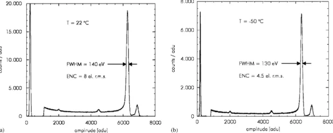
noise charge of 8 el. rms at room temperature (Fig. 10a) has been deduced. Moderate cooling to 50
C reduces the parallel noise contribution of the leakage current and results in an ENC of 4.5 el.
rms (Fig. 10b). In a single-pixel measurement incomplete charge collection caused by charge splitting cannot be discriminated or corrected for.
Therefore, the spectra show a pronounced low- energy background, and the width of the Mn-K lines is broadened by this effect as well.
3.4. Active pixel sensor
The matrix-like formation of DEPFETs with common back contact results in a backside illuminated Active Pixel Sensor (APS) with a unity fill factor. The thickness of the depleted bulk is 500 mm, increasing the quantum efficiency at the high energy end compared to pn-CCDs (see Fig. 6), e.g. 96% at 10 keV, 45% at 20 keV. On the low energy side the quantum efficiency values can be taken from the pn-CCD data (Fig. 6) as the same thin entrance window technology is applied.
All DEPFETs in the pixel sensor have a common drain contact, while the gates, clear contacts, and clear gates are connected row-wise and the source contacts, i.e. the signal lines, are connected within each column. That way the pixel matrix is read and cleared row-wise, the readout is
done in parallel for all columns. Small prototype sensors of this type with 64 64 pixels have already been fabricated and applied in biomedical applications as imagers with limited energy resolu- tion [34].
In its proposed layout the XEUS focal plane detector will be composed of 1024 1024 DEP- FETs with a pixel size of 75 75 mm
2resulting in a total area of 7.68 7.68 cm
2. Due to the diffusion- dominated extension of signal charge packages along their drift to the internal gates, about 70%
of the photons will hit more than one pixel.
Therefore, the coordinates of the photons’ inter- action can be reconstructed by the centroid method with a precision considerably better than the pixel size. The position resolution is in any case better than 20 mm, and in the optimal case when the photon hits exactly the pixel border it is 4 mm.
The energy of these split events can be recon- structed by pixel summation.
The proposed APS for the XEUS Wide Field Imager consists of 16 sections each having a size of 128 512 pixels (Fig. 11). Analogue to the XMM–
Newton pn-CCD array (see Fig. 3) the division into sections is purely logic. The full detector area is sensitive without any dead space between the subunits. All readout and reset operation steps mentioned above are applied to all sections simultaneously. To selectively activate a row of
Fig. 10. Spectra of a radioactive55Fe source recorded with a single DEPFET at room temperature (a) and at 50C (b). The spectra are not energy calibrated but in ADC units (adu).
pixels for readout or reset control chips of the SWITCHER type [34] in a high-voltage CMOS technology are connected along the left and right sides to the matrix in Fig. 11. From the left side one (horizontal) row of pixels is selected for readout. This is achieved by applying an appro- priate gate voltage to all pixels of this row, which turns on the transistor currents. From the other side a clear pulse can be sent to a selected row. The control chips are identical, however a dedicated
voltage supply and timing scheme has to account for either clearing or readout. The sections of the upper and lower detector halves are read out simultaneously in opposite directions. Each col- umn, i.e. 512 pixels, of a section is fed into one channel of a modified preamplifier chip of the CAMEXtype.
As the individual pixels are random accessible, the APS has a high degree of flexibility in the choice of readout modes depending on the object and the scientific goal of an observation: in full frame mode the whole sensor area is read row by row. With the exception of one active row, all pixels are turned off and in integration mode, thus keeping dead time short and power consumption low. The processing time for one row is of the order of a few micro-seconds. The whole sensor is read within milli-seconds. In window mode only selected regions of interest (ROIs) that may have arbitrary rectangular shapes and sizes are read out, while the other pixels are suppressed. Time variations of fast transients will be observed in timing mode, i.e. a selected ROI is read at maximum speed but with reduced energy resolu- tion. A limited area of 32 pixel rows or 2.5 mm in the readout direction could then be processed up to count rates of 10
5s
1. Any combination of the above specified readout modes or mixed mode applied to dedicated regions of the sensor area is possible.
At present 64 64 APS prototypes are in production. First samples of the SWITCHER control chips and CAMEXpreamplifier chips have been tested successfully.
3.5. Repetitive non-destructive readout
In a DEPFET the signal charges are strictly confined in a potential well. The information, i.e.
the number of charges in the internal gate, is not destroyed during the readout so that multiple reads of the same signal with subsequent averaging is possible. Repetitive readout results in a reduc- tion of the 1/f noise contribution by n
1/2, with n the number of independent readings. It has already been demonstrated that this technique allows spectroscopy measurements with sub-electron pre- cision [35].
Fig. 11. Layout of the XEUS Wide Field Imager focal plane with an Active Pixel Sensor. The 10241024 pixels are switched on and off and reset row-wise by SWITCHER control electronics units at the left and right sides. The vertical channels of the APS are read out in parallel by CAMEXamplifier/
multiplexer chips at the bottom and topside.
The technique of repetitive non-destructive readout is best realized by the combination of two DEPFETs within one pixel and the lateral intra-pixel charge transfer between the two inter- nal gates. That way one of the DEPFETs reads the signal while the other one reads the baseline value of the empty internal gate. Moreover, connecting the signal lines of the two DEPFETs to the inputs of differential amplifier reduces the practical problem of common mode fluctuations. Fig. 12 shows the possible layout of such a ‘ping pong’
DEPFET, in which the signal electrons are shifted across the common drain of the two transistors.
Devices of this type are currently in production.
4. Conclusion
Both derived from the basic principle of side- ward depletion pn-CCDs and DEPFET based Active Pixel Sensors unify the contradictory requirements of X-ray astronomy for imaging spectrometers: high-energy resolution, high quan- tum efficiency, two-dimensional position resolu- tion, large sensitive area, low power consumption, and fast readout. While pn-CCDs have proven their superior performance and reliability during 3
years onboard the European satellite XMM-New- ton, the DEPFET is a promising option for the future to avoid the CCD inherent handicaps connected to the need of charge transfer inside the detector bulk. A DEPFET based Active Pixel Sensor is a candidate for the Wide Field Imager of the future XEUS mission.
Acknowledgements
The successful development of detectors was only possible through the effort of the complete staff of MPI-Halbleiterlabor and the close rela- tions to the mother institutes MPI f ur extraterres- . trische Physik and MPI f ur . Physik. The collaborations with colleagues at Politecnico di Milano, Italy, Institut f. ur Astronomie und Astro- physik in T. ubingen, Germany, University Bonn, Germany, and Brookhaven National Laboratory, USA, have been a pleasure.
The simulation software POSEIDON was de- veloped by A. Castoldi, E. Gatti, and P. Rehak within the INFN-RIMAXproject.
References
[1] R. Giacconi, H. Gurski, F.R. Paolini, B.B. Rossi, Phys.
Rev. Lett. 9 (1962) 439.
[2] S.L. O’Dell, M. Weisskopf, Proc. SPIE 3444 (1998) 2.
[3] ESA project ‘‘XMM’’, ESA Bulletin (special issue) 100 (1999) 1.
[4] H. Wolter, Ann. Phys. 10 (1952) 52.
[5] B. Aschenbach, Rep. Prog. Phys. 48 (1985) 579.
[6] A.D. Holland, Nucl. Instr. and Meth. A 377 (1996) 334.
[7] M.L. van den Berg, A.J.F. den Boggende, T.M.V. Boot- sma, J.W. den Herder, F.A. Jansen, P.A.J. de Korte, E.J.
van Zwet, T. Eaton, R. Ginige, Nucl. Instr. and Meth. A 377 (1996) 313.
[8] L. Struder, P. Holl, G. Lutz, J. Kemmer, Nucl. Instr. and. Meth. A 253 (1987) 386.
[9] L. Struder, P. Holl, G. Lutz, J. Kemmer, Nucl. Instr. and. Meth. A 257 (1987) 594.
[10] V. Radeka, P. Rehak, S. Rescia, E. Gatti, A. Longoni, P.
Holl, L. Struder, J. Kemmer, J. Phys. 49 (9) (1988) 363.. [11] V. Radeka, P. Rehak, S. Rescia, E. Gatti, A. Longoni, P.
Holl, L. Struder, J. Kemmer, IEEE Electron Device Lett.. 10 (2) (1989) 91.
[12] E. Pinotti, et al., Nucl. Instr. and Meth. A 326 (1993) 85.
[13] H. Brauninger, R. Danner, N. Findeis, D. Hauff, P. Holl,. J. Kemmer, E. Kendziorra, J. Kramer, P. Lechner, G.. Fig. 12. ‘Ping Pong’ DEPFET for repetitive non-destructive
readout. The intra-pixel transfer between the internal gates of the two linear DEPFETs allows the repeated independent reading of physically the same information, thus reducing the read noise by the square root of the number of readings.
Lutz, N. Meidinger, M. Mohan, E. Pinotti, C. Reppin, R.
Staubert, L. Struder, J. Tr. umper, C. von Zanthier, The. XMM pn-CCD Detector System—First Results, ESA Publication Division SP 356 (1992) 69.
[14] H. Brauninger, et al., Metrologia 32 (1995) 643.. [15] H. Soltau, et al., Nucl. Instr. and Meth. A 377 (1996) 340.
[16] P. Holl, et al., Proc. SPIE 3114 (1997) 126.
[17] N. Meidinger, et al., Proc. SPIE 3765 (1999) 192.
[18] H. Soltau, et al., Nucl. Instr. and Meth. A 439 (2000) 547.
[19] L. Struder, et al., Rev. Sci. Instrum. 48 (11) (1997) 4271.. [20] E. Gatti, P. Rehak, Nucl. Instr. and Meth. A 225 (1984)
608.
[21] W. Buttler, G. Lutz, G. Cesura, P.F. Manfredi, V. Speziali, A. Tomasini, Nucl. Instr. and Meth. A 326 (1993) 63.
[22] H. Gajewski, TeSCA Handbook, WeierstraX-Institut fur. angewandte Analysis und Stochastik, Berlin, Germany.
[23] L. Struder, et al., Nucl. Instr. and Meth. A 288 (1990) 227.. [24] L. Struder, B. Aschenbach, H. Br. auninger, G. Drolshagen,. J. Englhauser, R. Hartmann, G. Hartner, P. Holl, J.
Kemmer, N. Meidinger, M. Stubig, J. Tr. umper, Astron.. Astrophys. 375 (2001) L5.
[25] N. Meidinger, B. Aschenbach, H. Brauninger, G. Drol-. shagen, J. Englhauser, R. Hartmann, G. Hartner, R.
Srama, L. Struder, M. St. ubig, J. Tr. umper, Experimental. verification of a micrometeoroid damage in the PN-CCD camera system aboard XMM-Newton, Proc. SPIE 4851 (2002).
[26] The XEUS Astrophysics Working Group (XAWG), X-ray Evolving Universe Spectroscopy—The XEUS Science Case, ESA SP 1238 2000 30.
[27] E.R. Fossum, Proc. SPIE 1900 (1993) 2.
[28] G. Prigozhin, S. Kissel, M. Bautz, C. Grant, B. LaMarr, R. Foster, G. Ricker, G. Garmire, Proc. SPIE 4012 (2000) 720.
[29] J. Kemmer, G. Lutz, Nucl. Instr. and Meth. A 253 (1987) 356.
[30] J. Kemmer, G. Lutz, U. Prechtel, K. Schuster, M. Sterzik, L. Struder, T. Ziemann, Nucl. Instr. and Meth. A 288. (1990) 92.
[31] P. Klein, G. Cesura, P. Fischer, G. Lutz, W. Neeser, R.H.
Richter, N. Wermes, Nucl. Instr. and Meth. A 392 (1997) 254.
[32] V. Radeka, The ‘ktC Noise’—equipartition, fluctuation- dissipation and detection sensitivity, Proceedings of the ninth European Semiconductor Detector Symposium, 2002, Nucl. Instr. and Meth. to be published.
[33] A. Castoldi, E. Gatti, P. Rehak, IEEE Trans. Nucl. Sci.
NS-43 (1996) 256.
[34] P. Klein, T. Aurisch, P. Buchholz, P. Fischer, M. Locker,. W. Neeser, L. Struder, M. Trimpl, J. Ulrici, J. Vocht, N.. Wermes, Nucl. Instr. and Meth. A 454 (2000) 152.
[35] R.P. Kraft, D.N. Burrows, G.P. Garmire, J.A. Nousek, J.R. Janesick, P.N. Vu, Nucl. Instr. and Meth. A 361 (1995) 372.

![Fig. 2. Electron potential of a pn-CCD simulated by the two-dimensional device simulator TeSCA [22]](https://thumb-eu.123doks.com/thumbv2/1library_info/3999337.1540355/4.816.80.749.128.645/fig-electron-potential-simulated-dimensional-device-simulator-tesca.webp)