Doctoral Thesis
The MYTHEN III Detector System - A single photon-counting microstrip detector for powder diffraction experiments
Author(s):
Andrä, Marie Publication Date:
2021-01
Permanent Link:
https://doi.org/10.3929/ethz-b-000462676
Rights / License:
In Copyright - Non-Commercial Use Permitted
This page was generated automatically upon download from the ETH Zurich Research Collection. For more information please consult the Terms of use.
The MYTHEN III Detector System
A single photon-counting microstrip detector for powder diraction experiments
A thesis submitted to attain the degree of DOCTOR OF SCIENCES of ETH ZURICH
(Dr. sc. ETH Zurich) presented by MARIE ANDRÄ MSc Physics, ETH Zurich
born on 2. May 1993 citizen of Germany
accepted on the recommendation of Prof. Dr. S. Johnson
Dr. B. Schmitt
2021
I hereby declare that the following submitted thesis is original work which I alone have authored and which is written in my own words.
Title: The MYTHEN III Detector System - A single photon-counting microstrip detector for powder diraction experiments
Author: Marie Andrä
Supervisors: Prof. Dr. S. Johnson, Dr. B. Schmitt
With my signature I declare that I have been informed regarding normal aca- demic citation rules and that I have read and understood the information on Ci- tation etiquette. The citation conventions usual to the discipline in question here have been respected. Furthermore, I declare that I have truthfully documented all methods, data, and operational procedures and not manipulated any data. All persons who have substantially supported me in my work are identied in the ac- knowledgements and contributions. The above work may be tested electronically for plagiarism.
Zürich, November 9, 2020
The development of X-ray detectors is essential for almost all elds of research using synchrotron radiation. With more powerful synchrotrons and X-ray Free Electron Lasers, the need for new detectors becomes more evident in order to extend the current limits. The new detectors must be able to cope with high photon ux, allow for fast, time-resolved measurements and cover a large energy range for the huge variety of experiments in the elds of material science, biology or chemistry. Moreover, the spectral resolution and noise should be as narrow as possible to allow the access of low X-ray energies.
The photon counting microstrip detector MYTHEN III was developed at the Swiss Light Source to respond to these demands in the eld of time-resolved powder diraction experiments. It is based on Silicon strip sensors with a pitch of 50µm, covers an angular range of 120◦ with a resolution of 0.004◦ and features three counters per strip.
The goal of this work is to characterise the performance of the prototypes in order to dene the specications of MYTHEN III and nally test the results on the detector modules. Energy calibrations in monochromatic X-ray beams reveal the noise, gain and intrinsic response dispersion, while rate scans determine the maximum detectable photon ux. The newly implemented interpolation mode of MYTHEN III allows to suppress charge sharing between neighbouring strips and improves the spatial resolution, while the dedicated negative polarity circuitry opens the opportunity to use high-Z material sensors for energies above30 keV or Low Gain Avalanche Detector sensors for very low energies.
With a minimum noise of114 electrons, MYTHEN III can detect energies down to 4.2 keV. At the same time, the selectable gain enables the detection of up to 180 keV signals. The low threshold dispersion of 20 eV yields a homogeneous response of the detector and simplies the data correction of the experiment. The maximum count rate at90 % detection eciency is determined to be3.5 MHzand can be extended to a multiple by pile-up tracking of the signal using the three counters.
The gures of merit of MYTHEN III meet all specications required for suc- cessful operation in the upgraded Swiss Light Source 2. The new detector enables faster time-resolved experiments at high photon ux and lower energies than its predecessor MYTHEN II and it opens many new possibilities for experiments in a wide eld of applications.
Die Entwicklung von Detektoren für Röntgenstrahlung ist maÿgebend für viele For- schungsbereiche, in denen Synchrotronstrahlung verwendet wird. Die zunehmende Brillianz der Synchrotron-Quellen geht einher mit der Notwendigkeit, neue Detek- toren zu entwickeln, um höhere Photonenüsse zu messen und schnelle, zeitauö- sende Messungen zu ermöglichen. Diese neuen Detektoren müssen einen grossen Energiebereich abdecken können, um der grossen Vielfalt von Experimenten ge- recht zu werden.
Des Weiteren ist die Optimierung der Energieauösung notwendig, um auch Experimente bei niedrigen Strahlenergien zu ermöglichen.
Der photonenzählende Streifendetektor MYTHEN III wurde an der Synchro- tron Lichtquelle Schweiz entwickelt, um genau diese Bedürfnisse im Bereich der zeitauösenden Pulverdiraktionsexperimente (Debye-Scherrer Verfahren) zu er- füllen. Er basiert auf Streifensensoren aus Silizium mit einer Streifenbreite von 50µm, deckt einen Winkelbereich von 120◦ ab, mit einer Auösung von 0.004◦, und besitzt drei Zähler in jedem Streifen.
Die vorliegende Forschungsarbeit erörtert das Verhalten der Prototypen, so- wie der nalen MYTHEN III Module. Energiekalibrierungen mit Hilfe von mo- nochromatischer Strahlung erlauben es, das Rauschen und die Homogenität des Detektors zu bestimmen. Ein Zählratenversuch zeigt ausserdem, wie hoch der ma- ximale Photonenuss sein darf, um den zuverlässigen Betrieb des Detektors zu ge- währleisten. Der Interpolationsmodus des Detektors ermöglicht die Unterdrückung von Ladungsteilung zwischen zwei benachbarten Streifen und verbessert somit die räumliche Auösung. Darüber hinaus können dank des implementierten Schalt- kreises für negative Ladungssammlung auch andere Sensormaterialien wie zum Beispiel GaAs oder CdTe benutzt werden, um den Energiebereich zu erweitern.
Mit einem kleinen Rauschen von 114 Elektronen, liegt die tiefste messbare Strahlenergie bei 4.2 keV. Gleichzeitig ermöglicht die einstellbare Verstärkung der Signale, Messungen von Photonen mit Energien bis zu180 keV. Die schmale Streu- ung der Schwellen von nur20 eV verspricht ein homogenes Verhalten des Detektors und erleichtert im Experiment die Datenverarbeitung. Unter Annahme einer aus- reichenden Ezienz von 90 %, liegt die höchst mögliche Zählrate pro Kanal bei 3.5 MHz. Diese kann mithilfe der drei Zähler um ein Vielfaches erhöht werden, indem die Überlagerung von mehreren Signalen im Sensor registriert wird.
Die Merkmale von MYTHEN III erfüllen alle Anforderungen für einen erfolg- reichen Einsatz an der aufgerüsteten Synchrotron Lichtquelle Schweiz 2. Dieser
dadurch viele Möglichkeiten für neuartige Experimente in der Pulverdiraktion.
I thank all the people who helped and supported me during my PhD from the bottom of my heart.
First of all, I want to thank Prof. Steven Johnson for his supervision and great support during the last four years.
The whole project would not have had any chance of success without the SLS Detector Group. I am very thankful to Bernd Schmitt for all the fruitful dis- cussions, many explanations and critical questions and of course the opportunity to work on MYTHEN III. A big gratitude goes to Anna Bergamaschi for her overwhelming and patient supervision, answering all my endless questions, solving programming issues, teaching me a lot about detectors and various beamtimes. I also want to thank Aldo Mozzanica for help with wafer testing and general com- puter problems; Carlos Lopez Cuenca, Martin Brückner and Pawel Kozlowski for the rmware and many custom changes; Christian Ruder for his electronics sup- port, teaching me how to solder and wirebond and always being available for a chat; Davide Mezza for lessons in electronics and supply with coee; Dhanya That- til and Erik Fröjd for the detector software; Dominic Greienberg for discussions about detectors and data analysis; Gemma Tinti for physics discussions; Jiaguo Zhang for all his knowledge about sensors; Markus Meyer for our mini electron- ics course; Rebecca Barten for carefully dicing and picking the chips and sensors, and helping in all situations; Roberto Dinapoli for the chip design and according extensive explanations; Sabina Chiriotti for our running sessions; Seraphin Vet- ter for (often last-minute) mechanical solutions and inexhaustible encouragement;
Shqipe Hasanaj for detector mechanics; and Sophie Redford for correcting the whole group's English. It was a great joy to work with all of you.
I am grateful to Nicola Casati, Antonio Cervellino and Dominik Meister from the MS beamline for oering us so many beamtimes with great support and pa- tiently waiting for the detector. A warm thanks also to Valerio Scagnoli and Manuel Guizar Sicairos from the cSAXS beamline for enabling the rst applica- tion of MYTHEN III and helping to correct the section about the polarisation measurements.
Finally, I thank my family and friends for their support and encouragement, especially Martin for the daily cappuccino and lunch supply during home-oce times.
Abstract
Zusammenfassung Acknowledgements
List of Figures iv
List of Tables vi
1 Introduction 1
1.1 Scope of this work . . . 1
1.2 Evolution of X-ray science . . . 2
1.3 Production of X-rays . . . 2
1.3.1 X-ray Tube . . . 3
1.3.2 Synchrotron . . . 3
1.4 Interaction of X-rays with Matter . . . 5
1.4.1 Photo-electric Absorption . . . 6
1.4.2 Elastic and Inelastic Scattering . . . 6
1.5 Detection of X-rays . . . 7
1.5.1 Detector Technologies . . . 8
1.5.2 Detector Characteristics . . . 11
1.6 Measurement Techniques at Synchrotrons . . . 13
1.6.1 X-ray Powder Diraction . . . 14
1.6.2 Small Angle X-ray Scattering . . . 16
1.6.3 X-ray Emission Spectroscopy . . . 16
2 X-ray Hybrid Semiconductor Detectors 17 2.1 Semiconductor Sensors . . . 17
2.1.1 Basic Semiconductor Properties . . . 18
2.1.2 Sensor Production . . . 22
2.1.3 Signal Conversion . . . 22
2.1.4 Charge Collection . . . 23
2.1.5 LGADs . . . 24
2.2 Front End Electronics . . . 26
2.3 Interconnection of Front End Electronics and Sensor . . . 27
2.4 Microstrip Detectors . . . 28
2.5 Charge Integrating Detectors . . . 28
2.6 Photon Counting Detectors . . . 29
2.6.1 Noise in the Detector . . . 30
2.6.2 Charge Sharing . . . 33
2.6.3 Dead Time, Count Rate Capability and Pile-up . . . 34
2.7 Examples of X-ray Detectors . . . 36
2.7.1 Detector Development at PSI . . . 38
3 The MYTHEN III Detector 41 3.1 Motivation for the Development of MYTHEN III . . . 41
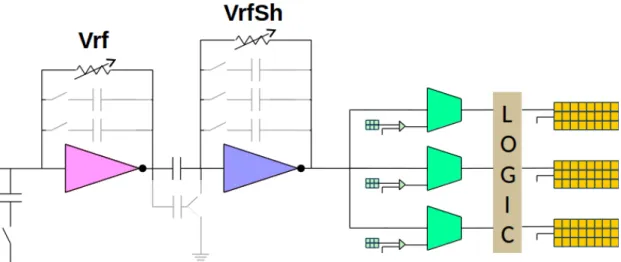
3.2 Architecture of the MYTHEN III Chips . . . 44
3.2.1 Modes of Operation . . . 47
3.2.2 Chip Readout . . . 50
3.2.3 MYTHEN III.0.1 . . . 51
3.2.4 MYTHEN III.0.2 . . . 51
3.2.5 MYTHEN III.0 . . . 52
3.3 Module and Detector Design . . . 53
3.3.1 Module . . . 53
3.3.2 Strip Readout Board . . . 53
3.3.3 Detector . . . 55
4 Detector Characterisation 57 4.1 Energy calibration, Gain and Threshold Dispersion . . . 58
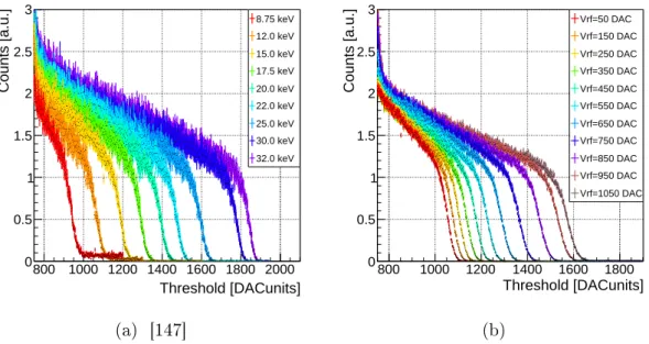
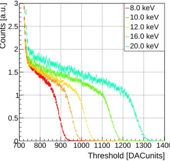
4.1.1 Threshold Scan . . . 58
4.1.2 Energy Calibration Method . . . 60
4.1.3 Threshold Dispersion Determination . . . 61
4.1.4 Calibration of MYTHEN III.0.1 . . . 62
4.1.5 Calibration of MYTHEN III.0.2 . . . 67
4.1.6 Conclusion from Prototype Testing . . . 71
4.1.7 Calibration of MYTHEN III.0 . . . 72
4.1.8 Calibration of a MYTHEN III module . . . 76
4.2 Trimming . . . 86
4.2.1 Trimming algorithm . . . 86
4.2.2 Trimming of MYTHEN III.0.1 . . . 87
4.2.3 Trimming of a MYTHEN III module . . . 89
4.3 Count Rate Capability . . . 93
4.3.1 Rate Scan Method . . . 93
4.3.2 Count Rate of MYTHEN III.0.1 . . . 95
4.3.3 Count Rate of MYTHEN III.0.2 . . . 97
4.3.4 Count Rate of a MYTHEN III module . . . 101
5 First Applications of MYTHEN III 105 5.1 Imaging with MYTHEN III . . . 105
5.1.1 2D Imaging Technique . . . 105
5.1.2 Imaging of the PSI Logo with MYTHEN III.0.1 . . . 107
5.1.3 Imaging of a Siemens star with a MYTHEN III module . . . 109
5.2 Powder Diraction Patterns with a MYTHEN III module . . . 110
5.3 Polarisation Measurements . . . 113
6 Characterisation of LGADs with MYTHEN II and GOTTHARD117 6.1 The Microstrip LGAD Sensors . . . 117
6.2 Leakage Current . . . 119
6.3 Energy Response . . . 120
6.4 Multiplication Factor . . . 122
6.5 Noise and Energy Resolution . . . 124
6.6 Fill Factor . . . 126
6.7 Tender X-ray Energy Dispersive Spectrometer Measurements . . . . 129
6.8 Discussion . . . 130
6.9 LGADs with MYTHEN III.0.2 . . . 131
7 Conclusion and Outlook 133 7.1 Concluding Performance of MYTHEN III . . . 133
7.2 Future of MYTHEN III . . . 137
7.3 Contributions . . . 139
Abbreviations 141 Appendix 145 A Chip Signals . . . 145
Bibliography 149
1.4.1 Attenuation coecient of Silicon . . . 7
2.1.1 PN-Junction . . . 20
2.1.2 Detection eciency in dierent materials . . . 24
2.1.3 Electron-induced impact ionisation . . . 26
2.6.1 Pile-up schema . . . 35
3.2.1 Schema of one strip in MYTHEN III . . . 45
3.2.2 Interpolation schema . . . 49
3.3.1 Module drawing . . . 54
3.3.2 Modules in the detector and full detector . . . 55
4.0.1 Picture of an adapterboard . . . 58
4.1.1 S-curve for dierent cases . . . 60
4.1.2 S-curves in MYTHEN III.0.1 . . . 62
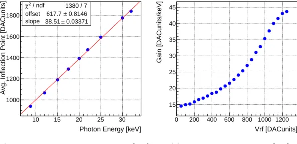
4.1.3 Calibration and gain of MYTHEN III.0.1 . . . 63
4.1.4 Average noise of MYTHEN III.0.1 . . . 64
4.1.5 Schema of edge scan . . . 65
4.1.6 Signal collection at dierent bias voltages . . . 66
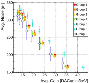
4.1.7 Average gains per group of MYTHEN III.0.2 . . . 68
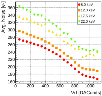
4.1.8 Average noise and gains per group of MYTHEN III.0.2 . . . 68
4.1.9 Multigains in MYTHEN III.0.2 . . . 70
4.1.10 S-curves in MYTHEN III.0 . . . 72
4.1.11 Calibration and gain in MYTHEN III.0 . . . 73
4.1.13 Threshold dispersion of MYTHEN III.0 . . . 74
4.1.14 Cross talk in HDI version 1 . . . 77
4.1.15 Cross talk in HDI version 2 . . . 78
4.1.16 Cross talk in HDI version 3 . . . 78
4.1.17 Module noise and gain in all HDIs . . . 79
4.1.18 Module gains at 20◦C . . . 80
4.1.19 Module noise and gain at 20◦C . . . 81
4.1.20 Module calibration at dierent temperatures . . . 82
4.1.21 Module gain at dierent temperatures . . . 83
4.1.22 Module threshold dispersion at dierent temperatures . . . 83
4.1.23 Module noise at dierent temperatures . . . 84
4.1.24 Module gain and noise at dierent temperatures . . . 85
4.2.1 Untrimmed and trimmed S-curves of MYTHEN III.0.1 . . . 88
4.2.2 Inection point dispersions in MYTHEN III.0.1 . . . 88
4.2.3 Trimmed and untrimmed S-curves in a module . . . 90
4.2.4 Trimming parameters . . . 92
4.3.1 Count rate and eciency in MYTHEN III.0.1 . . . 95
4.3.2 Dead time and noise in MYTHEN III.0.1 . . . 96
4.3.3 Rate eciency in MYTHEN III.0.2 . . . 97
4.3.4 Dead times in dierent groups of MYTHEN III.0.2 . . . 98
4.3.5 Comparison of rates at dierent settings in MYTHEN III.0.2 . . . 99
4.3.6 Comparison of noise vs. dead time in MYTHEN III.0.1 and III.0.2 . 100 4.3.7 Count rate eciencies of the module . . . 101
4.3.8 Module's noise and dead time . . . 102
4.3.9 Comparison of noise-dead time for all MYTHEN III chips . . . 103
4.3.10 Rate at 90 % eciency for many counters . . . 104
5.1.1 Microscope picture of the PSI logo . . . 107
5.1.2 Imaging setup . . . 107
5.1.3 Image of the PSI logo . . . 108
5.1.4 Image of a Siemens star . . . 109
5.2.1 Cu-oxalate diraction patterns . . . 112
5.3.1 Setup at cSAXS . . . 114
5.3.2 Polarisation of the beam . . . 115
6.1.1 LGAD cross section . . . 118
6.2.1 Dynamic range and leakage current in LGADs . . . 120
6.3.1 Energy response of LGADs . . . 121
6.4.1 LGAD response to 8.05 keV . . . 123
6.4.2 LGAD multiplication factor . . . 123
6.5.1 LGAD noise and energy resolution . . . 124
6.5.2 2.1 keV S-curve in a LGAD . . . 125
6.6.1 Fill factors in the LGAD . . . 127
6.6.2 LGAD-map of multiplication regions . . . 128
6.7.1 Sulphur emission spectrum . . . 129
6.9.1 LGAD on MYTHEN III.0.2 . . . 131
1.1 X-ray emission energies . . . 6
1.2 Imaging, diraction and spectroscopic techniques . . . 14
2.1 PSI detector developments . . . 39
4.1 Module HDI versions . . . 76
4.2 Comparison of dead times in MYTHEN III.0.2 . . . 99
4.3 Count rates in MYTHEN III module . . . 104
6.1 MYTHEN III.0.2: LGAD calibration . . . 132
7.1 Summary comparison of gures of merit . . . 136
A1 Chip Status Bits in MYTHEN III . . . 145
A2 DAC signals . . . 146
A3 Digital chip control signals . . . 147
Introduction
1.1 Scope of this work
This work presents the photon counting Microstrip sYstem for Time-rEsolved ex- perimeNts (MYTHEN) III and its gures of merit in terms of noise, gain, threshold dispersion and count rate capability. MYTHEN III also serves as a test system for design options and methods for a future 2D single photon counting pixel detector.
Since MYTHEN III is an X-ray detector, the work starts with a short in- troduction to X-rays (section 1.2), how they are produced in X-ray tubes or at synchrotrons (section 1.3) and continues with their interaction with matter (sec- tion 1.4). Section 1.5 reveals dierent methods to detect the X-rays, such that they can be used for dierent measurement techniques explained in section 1.6. The work continues with an overview of hybrid detector systems, consisting of a sensor (section 2.1) connected to the front end electronics (section 2.2) and presents some examples of X-ray detectors in section 2.7.
After this general introduction, the design of the MYTHEN III detector is discussed in detail, starting with the chip architecture in section 3.2 up to the full detector system (section 3.3). Finally, chapter 4 shows the characterisation results of the MYTHEN III prototypes which guided the chip designer towards optimal design choices for the full scale chip, whose gures of merit in terms of noise, gain, threshold dispersion and count rate capability are also presented. In addition, some applications of the MYTHEN III detector in chapter 5 prove its functionality and illustrate its imaging ability. A short excursus in chapter 6 demonstrates the potential of LGAD sensors to extend the use of X-ray detectors to much lower energies.
The thesis closes with a summary and thoughts about the future of MYTHEN III (chapter 7).
1.2 Evolution of X-ray science
The discovery of X-rays by Wilhelm Röntgen in late 1895 [1,2] revolutionised many elds of science like medicine, pharmacy, physics, chemistry or biology. While in the beginning the research of and with X-rays was dominated by physicists, they are meanwhile a widely used tool for research in almost all elds [1]. X-rays allow an insight into the internal structure of molecules and cells, to identify chemical compositions and fabrication techniques, and to non-destructively examine archae- ological artefacts and paintings [1].
Röntgen detected that a barium platinocyanide sheet placed next to a high- voltage discharge tube starts to uoresce even though the tube was enclosed in a cardboard box [1]. He concluded that the tube must emit an unknown form of radiation and named it X-rays. In his subsequent experiments, he exposed photographic plates to the radiation and took the rst X-ray image of the hand of his wife [1].
In the following years, Barkla and Sadler discovered the characteristic X-ray emission lines of the elements, Max von Laue recorded the rst diraction pattern of copper sulphate and the Bragg law was formulated, which forms the foundation of X-ray crystallography [1]. In parallel, William Coolidge developed the hot cath- ode tube where electrons needed to create X-rays are produced with a hot tungsten lament as cathode, which is heated by an electric current [3, 4]. This design is still the basic principle of today's modern X-ray tubes in many laboratories all around the world.
1.3 Production of X-rays
X-rays are produced from the conversion of kinetic energy of electrons to electro- magnetic radiation when they are decelerated or interact with matter [5]. Their energy E is given by
E = hc
λ (1.1)
with Planck's constanth=6.626·10−34J s, the speed of lightcand the wavelength λ. E ranges from 0.1 keV to several 100 keV, whereas X-rays with energies above around510 keV are called hard X-rays in contrary to the soft X-rays with lower energies. This classication is however not standardised and may dier in literature [1,6].
Each material has characteristic spectral lines, dened by the atomic electronic transitions. At these energies, the X-ray absorption suddenly increases and the re- emitted uorescence photons will have one of these energies, denotedKα1,2,Kβ1,3, Lα1,2, Lβ1 etc. (Siegbahn notation [7])1. The emission energies of some materials
1Transitions from the L-shell (i.e. second shell) to the K-shell (lowest energy level) are named Kα1,2and transitions from the M-shell to the K-shell are namedKβ1,3. Analogously, transitions from the M-shell to the L-shell are called Lα, Lβ etc. [7, 8]. The integer indices specify the spin-orbit interaction energy. TheKα1andKα2 energies are so close that they are often quoted
are given in table 1.1.
There are three main sources of X-rays, namely the X-ray tube and the more powerful synchrotron, as well as the X-ray Free Electron Laser. Both continuously emitting sources are explained in this section, while a detailed description of X-ray Free Electron Lasers (XFELs) can be found in [1].
1.3.1 X-ray Tube
An X-ray tube consists of a cathode and an anode that are enclosed in a vacuum tube. The electrons are emitted by a heated tungsten lament that acts as cath- ode. The applied high voltage between the electrodes accelerates the electrons towards the anode, where they hit and interact with a target surface. The ki- netic energy loss during the abrupt deceleration of the electrons is then emitted as Bremsstrahlung. Another eect of the interaction between electrons and the tar- get metal is its ionisation and the caused uorescence, leading to the emittance of characteristic X-rays. The spectrum emitted by the X-ray tube is thus a superpo- sition of the continuous Bremsstrahlung and the characteristic uorescence lines of the target material [10]. Typical target materials include tungsten, molybdenum, chromium or copper. The maximum X-ray energy is given by the applied voltage between cathode and anode as it limits the acceleration of the electrons and thus their kinetic energy that can be converted into radiation. Typically, voltages of tens of kV are applied. The intensity of the photon ux is proportional to the current owing between the electrodes, which is in the order of some mA [5].
In order to dissipate the heat created during the absorption process, modern X-ray tubes are either water cooled or have a rotating target anode (mainly high power machines), such that only a small part is hit by the electrons while the rest of the target can cool down [5,10]. The target surface is tilted by720◦ towards the exit window of the tube and its area as well as the angle determine the eld-of-view of the emitted photon beam [5].
For many measurements, monochromatic X-rays are required. In common lab- oratory diractometers, monochromators or Kβ-lters are used to achieve mono- energetic beams. Alternatively, for detector characterisations, X-ray tubes can be operated in combination with uorescence targets that are excited by the white photon beam and re-emit photons only at their characteristic uorescence ener- gies. With additional Kβ-lters, a single uorescence line can be chosen while all other energies will be blocked, such that the resulting photon beam is (quasi) monochromatic.
1.3.2 Synchrotron
With evolving research, stronger sources of X-rays were developed, namely the synchrotrons. Synchrotron radiation is emitted when a charged particle travel- ling at relativistic speed is accelerated. This eect is used in synchrotrons, where
asKα [9].
electrons generated in an electron gun are pre-accelerated in a linear accelerator to about 100 MeV and injected into a booster ring, where they are further ac- celerated to the same energy as the electrons in the storage ring (1.78 GeV for third-generation facilities) [1]. The relativistic electrons are then injected into the storage ring where they are maintained on a close path by an array of magnets.
At each arced section of the ring, the bending dipole magnets force the electrons to change their path to follow the orbit, while quadrupol and sextupole magnets refocus the beam to reduce its divergence. During the bending, the electron beam emits synchrotron radiation (Bremsstrahlung) tangentially to its orbit. This ra- diation is used for experiments at bending-magnet beamlines. At the straight sections in between the bending magnets, insertion devices are used to generate high-brilliance synchrotron radiation. They consist of an array of alternating po- larity dipole magnets forcing the electrons on a oscillatory path and hence causing the emission of synchrotron radiation. There are two types of insertion devices:
wigglers and undulators [1]. In a wiggler, the angular excursion of the electrons from their path is large which leads to high energetic photons with a continuous spectrum. In an undulator, the period of dipoles is reduced, and hence the excur- sions are gentler. Therefore, the narrower radiation cones interfere with each other and only a discrete set of wavelengths is emitted at lower photon energies [1,11,12].
For both devices, the emitted radiation is polarised and partially coherent and typ- ically arrives in bunches of around 20100 ps given by the length of the electron bunches, spaced by some few to hundred nanoseconds [1].
The energy loss of the electron beam due to the distraction in the curved section and the insertion devices is compensated for by radio frequency cavities along the track which supply the electrons with just the amount of energy they lost previously, such that the electron beam stays on its orbit.
The last component of a synchrotron are its tangential beamlines placed at the bending magnets and insertion devices, where the synchrotron radiation is used for experiments. Since beamlines are optimised for dierent kind of experiments, their composition behind the front end varies. However, typically the beam is focussed and monochromatized (with a bandwidth of around ∆EE ∼ 10−4) by the beamline's optics before it reaches the experimental hutch [1].
The rst synchrotron radiation from a cyclotron was observed in 1947 at the General Electric Research Laboratory in New York [1]. However, it took an- other 14 years until the National Bureau of Standards in Washington modied its 180 MeV electron synchrotron to access the X-radiation. Thus the rst generation of synchrotrons was born [1].
In 1963, the Fermi National Accelerator Laboratory built a high-energy ac- celerator near Chicago and in 1964 the range of synchrotron radiation was ex- tended signicantly with the commissioning of the 6 GeV Deutsches Elektronen Synchrotron (DESY) in Hamburg (Germany) used for high-energy physics and production of synchrotron radiation [1]. Second generation sources optimised for radiation emission where built shortly after. The rst one, the2 GeV Synchrotron Radiation Source (SRS) started its operation in 1981 in Daresbury (England).
The development of insertion devices allowed the development of third generation sources optimised for brilliance [1]. The rst built was the European Synchrotron Radiation Facility (ESRF) in 1994 in Grenoble (France). Today, there are several third generation synchrotron facilities all over the world, some of which will be upgraded to the fourth generation within the next years. The fourth generation of synchrotrons, called Diraction Limited Storage Rings (DLSR), is based on stor- age rings with ultra low emittance, i.e. highly intense and parallel beam [1]. MAX IV in Lund (Sweden), was the rst fourth-generation machine to start operation in 2016 [1].
Swiss Light Source
The Swiss Light Source (SLS) is a third generation synchrotron located at the Paul Scherrer Institute in Switzerland, where this work is performed. The project was approved in 1997 and commissioning of the SLS was completed in 2001 [13, 14]. The storage ring has a circumference of 288 m with 36 bending mag- nets and operates with a 2.4 GeV electron beam at 400 mA with a brilliance of 4·1019ph/s/mm2/mrad2/0.1% BW. It has 16 operational user-beamlines with a great variety of energy ranges and applications [15]. The SLS will be upgraded to a fourth generation facility in 2023-2026 [16].
1.4 Interaction of X-rays with Matter
The interaction of X-rays with matter is essential for all measurements performed with synchrotron radiation and especially for the detection of it. In general, most2 interactions of electromagnetic radiation with matter result in the attenuation or absorption of the beam [1]. The massless, electrically neutral photons travel at the speed of light and penetrate deeply into the matter where they interact mainly with the outer shell electrons of the atoms and eventually deposit their energy at one point. For most processes, during the passage of matter, the photon beam does not degrade in energy, but only attenuates in intensity because the underlying interaction processes remove entire photons from the beam, while the remaining photons pass through the matter without any interaction [17]. Only in inelastic Compton scattering events, the photon energy diminishes. The attenuation of the beam with initial intensity I0 is exponential with respect to the travelled distance x through the material [17]:
I =I0e−µx (1.2)
with the absorption coecient µ= ρNAAσa as a function of the material's density ρ, Avogadro's number NA = 6.022·1023/mol, the atomic mass A and the atomic absorption cross section σa [1].
For the considered energy range, there are two major interaction mechanisms contributing to the absorption coecient for X-rays in matter: photoelectric ab-
2There are also exceptions. X-ray lasers for instance will amplify the beam.
Element Kα1 [keV] Kβ1 [keV] K-edge [keV]
Titanium (Ti) 4.51 4.93 4.98
Iron (Fe) 6.40 7.06 7.13
Copper (Cu) 8.05 8.90 8.99
Molybdenum (Mo) 17.48 19.61 20.01
Indium (In) 24.21 27.28 27.95
Table 1.1: X-ray emission line energies and K-edge level for some materials. With data from [18].
sorption and Compton scattering [17], while diraction of X-rays is based on elastic scattering.
1.4.1 Photo-electric Absorption
In the photo-electric eect, a photon is absorbed by an atomic electron with the subsequent ejection of a photoelectron from the atom [17]. Momentum conserva- tion forbids the absorption of a photon by a free electron, therefore this interaction is only possible with bound electrons with the nucleus absorbing the recoil mo- mentum [17]. The electron can only be ejected if the photon energy exceeds the binding energy of the electron. The stronger the electron is bound, the higher is the absorption probability, i.e. K-edge absorption is more likely than L-edge absorption, while absorption by a free electron is impossible as the conservation of momentum is not satised [6, 17]. Its energy is given by Ee− =hν−Eb where h is Planck's constant, ν is the photon's frequency and Eb is the binding energy of the shell electron. The ejected photoelectron leaves a vacancy in the atomic shell which is quickly lled either through the capture of a free electron or by rearrangement of electrons from outer shells. If an electron from the outer shell falls into the vacancy, it will release its excess energy in form of a characteristic uorescence photon or transfer it to an outer shell electron causing the emission of an Auger electron [6]. Some characteristic emission lines are given in table 1.1.
The photo-electric eect is dominant for the energy range of synchrotron radiation.
1.4.2 Elastic and Inelastic Scattering
With increasing photon energy, the elastic (Thomson) and inelastic (Compton) scattering becomes more important in the interaction process.
In the Compton scattering process, an incoming X-ray is deected by an elec- tron of the absorbing material and transfers part of its energy to the electron [6].
The energy of the outgoing photon at a scattering angle θ will be:
hν0 = hν
1 + mhν
0c2 (1−cosθ) (1.3)
Photon Energy [keV]
1 10 102
/g]
2Attenuation [cm
−2
10
−1
10 1 10 102
103
104
Total Attenuation Thomson Scattering Compton Scattering Photoelectric Absorption
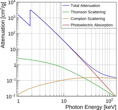
Figure 1.4.1: The attenuation coecient for Silicon as function of the photon energy.
The photoelectric absorption dominates the process up to 60 keV. At the K-edge of Silicon (1.84 keV), the absorption drops. With data from [18].
with the rest-mass energy of the electron m0c2 = 0.511 MeV. The probability of Compton scattering increases linearly with the number of available electrons, i.e. with Z [6]. In the case of non-relativistic energies hν m0c2, no energy is transferred between the electron and the photon and the scattering process is elastic (Thomson scattering).
Figure 1.4.1 shows the total attenuation coecient, as well as the photoelectris and scattering contributions, as function of the photon energy for silicon. The absorption is high for energies just above the K- or L-edge, where many photons can excite an electron, and much lower just below the edge.
1.5 Detection of X-rays
Synchrotron science relies on the fast and precise detection of X-rays. Hence, detection methods and detector development are essential to perform and push X- ray science beyond its current limits. With the increasing number of synchrotrons and hence great diversity of innumerable X-ray experiments conducted, the re- quirements for detectors are manifold and consequently there are meanwhile many dierent X-ray detectors available.
In early days, photographic lms were sucient for the rst X-ray experiments, but soon, Geiger-Müller tubes, image plates, Charge Coupled Devices (CCDs),
scintillators and gas detectors took over [1]. The development of semiconductors in the 1970s allowed to convert X-rays directly into electrical charge, which lead to a breakthrough in detector development. The rst Silicon detectors were presented at CERN in 1980 and 1994, respectively [19, 20]. These semiconductor hybrid detectors evolved quickly, and developments dedicated to X-rays have spun o from high-energy physics research.
Some of the most common detection methods and according detectors, each suitable for dierent elds of experiments, are presented in the following section, complemented by the requirements posed on them.
1.5.1 Detector Technologies
Image Plates
Image plates are based on a storage phosphor screen [1], where a thin layer of phosphor, mixed with an organic binder, is deposited on a plastic substrate [6].
Ionising radiation absorbed in the phosphor creates secondary electrons that are trapped close to the interaction site. Hence, a latent image of the stored charge carriers is formed which can reproduce the spatial pattern of the incident radiation.
After the X-ray exposure, readout is carried out by scanning a nely focused laser across the whole plate [6]. The laser triggers the release of visible photons which are transported via optical bres to a photomultiplier [6]. Recording the light intensity as function of the laser position yields a digital image of the initial pattern [1,6]. After the readout, the image plate has to be reset. An advantage of image plates is the large linear dynamic range of105 and their spatial resolution of 100200µm, only limited by the scattering and diusion of the laser light within the phosphor layer [6]. However, the scan times are very long compared to modern semiconductor detectors and, therefore, time resolved experiments are not easily possible.
Scintillator Detectors
Scintillator detectors rely on the (partial) conversion of the absorbed X-rays into visible light, which is then amplied and detected by photomultiplier tubes [1].
The absorbed photon electrically excites the detection material, which rapidly transfers the energy to nearby states of the dopant ion. These relax by non- radiative processes to much lower states close to the nal relaxed state, which is reached by the emission of a photon in the visible light regime [1]. Typical inorganic materials used are salts or metal oxides doped with high-Z materials [1].
The most common are NaI(Tl) and YAP(Ce). The former has a very good x-ray stopping power and scintillates at maximum 415 nm, however, its drawbacks are the softness and sensitivity to moisture as well as the long recovery time of250 ns, which corresponds to a maximum count rate of 1 MHz. YAP(Ce) has a reduced eciency, but is mechanically robust and has a shorter recovery time of only 25 ns [1]. The visible light from scintillator plates can be guided to photosensitive
elements such as CCDs, photomultiplier tubes or photo-transistors to record X-ray images. The thickness of the material aects the eciency, i.e. the signal strength, which has to be traded-o against the declining spatial resolution [1].
Gas Detectors
The basic conguration of a gaseous ionisation detector is a container with con- ducting walls, a thin endwindow and a wire across its axis acting as anode [17].
The container is lled with a gas, typically a noble gas such as Argon or Xenon.
Radiation penetrating the container will ionise the gas molecules and create elec- tron ion pairs. The number of charge carriers is proportional to the energy and amount of radiation [17]. An electric eld applied between the walls and the on- axis wire accelerates the electrons towards the anode and the ions to the cathode, such that a current can be measured, proportional to the applied voltage and energy of the radiation. Depending on the applied voltage, the device is named ionisation chamber, proportional counter or Geiger-Müller counter [17]. In an ion- isation chamber, the voltage is just strong enough to separate the freed electrons from the ions produced by the radiation before they recombine. With increasing voltage, the free electrons are accelerated so much that they have enough energy to further ionise the gas molecules and create small avalanches. Nevertheless, the number of electron ion pairs in the avalanche remains proportional to the incoming radiation and the multiplication factor is a function of the applied voltage. The detector is then a proportional counting chamber where the number of incoming photons as well as their energy can still be quantied [17]. Further increasing the voltage leads to a total amount of ionisation that distorts the initial electric eld and proportionality is lost. Due to the chain reaction of avalanches, the readout current saturates and a quenching gas must be inserted into the detector to restore an operational mode after each detection of radiation [17]. Modern gas detectors are pixellated (Gas Electron Multipliers (GEMs) [21], Micromegas [22]) and can provide spatial resolutions around 100µm(compared to mm of wire chambers).
Charge Coupled Devices
Charge Coupled Devices (CCDs) can be described as an array of coupled photo- sensitive capacitors forming the pixels [23] of less than 10µm. Light impinging on the CCD is converted into electrons that are accumulated in the according pixel during exposure [24]. The serial readout of the charges yields a digital image where the signal per pixel is proportional to its accumulated charge [1]. In order to detect higher energetic radiation such as X-rays, CCDs are commonly used in combination with a thin layer of scintillator material converting the X-rays into visible light that is then detected by the CCD [1]. Very fast CCDs operate at1 kHz frame rate, while others run at 110 Hz or less [1].CCDs typically require substan- tial cooling, some are cooled down to liquid nitrogen temperature, and commonly suer from a readout noise which increases at high readout speeds.
Modern CCDs work well in the visible light regime and usually have a thin
active region, such that they are well suited for soft X-rays or coupled to scin- tillators. Thus, they are widespread in imaging devices such as digital cameras, barcode readers or satellites [24], but also widely used in research and synchrotron science [1]. Therefore, there exists a large variety of highly specialised CCD de- tectors [1].
Crystal Analysers
Crystal analysers are widely used in one dimensional crystallographic measure- ments such as powder diraction. They consist of a high-quality crystal, e.g Sili- con (111), that is mounted on the detector arm and can be rotated [1]. The angle θC of the crystal relative to the sample is determined by the Bragg condition. If the interplanar distance within the crystal is dC and the energy of the used X-ray beam is given by Eγ, the angle must full [1]
sinθC = mhc
2EγdC (1.4)
where m is an integer, c the speed of light and h Planck's constant. With this angle, only elastically scattered photons will be diracted by the crystal towards the readout system while all other energies created e.g. by uorescence and also photons scattered by air outside the sample are ltered out. That is the reason why no additional slits are required to lter the X-ray beam. The eective equivalent of the slit width is in the order of 5µm. It is given by the crystal-sample distance and the rocking-curve of the analyser [1].
Point detectors like the crystal analyser are limited by their small eld of vision [1]. Thus, a scan of several positions must be performed to gain an intensity prole. Depending on the required angular range and statistics, measurements typically take between 15 minutes and several hours. On the other hand, crystal analysers have an excellent angular resolution and are therefore still used for high resolution powder diraction experiments.
Hybrid Strip and Pixel Semiconductor Detectors
In hybrid detectors, a semiconductor sensor is connected to a readout electronics.
This principle oers a large exibility since dierent sensors can be connected to a suitable front end electronic. Common sensor materials include Silicon, Germa- nium, Cadmium-Telluride or Gallium-Arsenide. Customised to the application, the sensors and electronics can be segmented into two dimensional pixels or one dimensional strips. The two most common readout designs are charge integrators or photon counters. Both principles, as well as the sensor specications, are ex- plained in more detail in chapter 2. In general, hybrid semiconductor detectors reach a high detection eciency, a large dynamic range and a high count rate.
Some examples of such detectors are presented in section 2.7.
1.5.2 Detector Characteristics
The general performance of an X-ray detector system is quantied by its gures of merit. These include the detection eciency, the Signal-to-Noise Ratio (SNR), the energy and spatial resolution, the dynamic range and the count rate capability.
Detection Eciency
The Quantum Eciency (QE) quanties the eciency of the sensor, i.e. how many of the incident photonsNin are absorbed (Nabs) in the sensitive volume and create electron hole pairs in the semiconductor [25,26]:
QE = Nabs Nin
. (1.5)
The QE is wavelength and material dependent.
For a detector, the Detective Quantum Eciency (DQE) denes the ratio of the SNR of incoming radiation and SNR of the detected signal [27, 28]. It thus takes into account the readout noise and is a measure of how eectively the system works in terms of detecting radiation [29,30].
Signal-to-Noise Ratio
The SNR in an application is given by the photon statistics and the SNR of the detector. It describes the quality of a measurement [27, 31] and is hence one of the most widely used parameters to characterise a detector [26, 29]. The intrinsic variation in the number of photons is given by the natural uctuations of the incoming photon ux, following Poisson statistics [6, 31, 32]. Therefore, a mean signal of N photons will have an uncertainty of√
N, resulting in a statistical SNR of
SN R = N
√N =√
N . (1.6)
The statistical SNR will increase with increasing signal height, i.e. amount of absorbed photons [1]. On the other hand, the readout electronics of the detector will contribute additional readout-noise to the signal, reducing the total SNR [32].
In spectroscopic photon science applications with a direct measurement of the energy, the detector SNR is dened as the signal pulse height divided by the noise, while in photon counting applications it is given by the signal divided by the background. The background has two contributions: false noise counts in the detector and background from photons. Ideally, the contribution from the detector is negligible such that the total SNR is only given by photon statistics. Therefore, big eort is invested into reducing the readout noise to a minimum to maximise the total SNR [33,34]. The noise sources of a detector are discussed in more detail in section 2.6.1.
Spectral Energy Resolution
The most important property of most X-ray detectors is their response to monochro- matic radiation. The energy resolution quanties the ability of the detector to dis- tinguish two photons whose energies lie close to each other. It is given by the Full Width Half Maximum (FWHM) or standard deviation σ of the measured pulse height distribution divided by its mean value and quoted in percent [6, 26, 27].
The width of the distribution reects the uctuations in number of charge carriers created from pulse to pulse and variations of the processing in the detector.
A photon with energy E0 creates on average N0 = Ek0 charge carriers in the sensor, where k is the conversion factor of the sensor material. The uctuation in the number of generated charge carriers σN is given by the Fano factor F and consequently the resolution is
σN N0 =
√F N0 N0 =
rF k
E0. (1.7)
It benets from large energies as well as small conversion factors. In semiconductor materials, the conversion factor is typically small and thus the resolution can be less than ∼1 % FWHM [6].
Beside statistical eects, the variations in pulse height also arise from a drift in the operating characteristics of the detector itself during the measurement, random noise in the detector or readout noise [6].
Position Resolution
The spatial resolution of a detector denes the minimum spatial distance needed between two photons so that they are still distinguishable [28, 35]. It is governed by the pixel granularity [32] and quantied by the Point Spread Function (PSF), Edge Spread Function (ESF) or Line Spread Function (LSF) in space domain or by the Modulation Transfer Function (MTF) or Contrast Transfer Function (CTF) in the frequency range [26,28,35]. Scintillators have a Gaussian PSF, while in a pixel or strip detector, the PSF can be modelled with a box response with the pixel size as limit [36]. The resulting standard deviation is
σ = p
√12 (1.8)
where p is the pixel or strip pitch. The spatial resolution can be increased by using charge sharing between neighbouring pixels as explained in [34]. Taking into account the charge sharing, the box-PSF transforms to a trapezium [36].
Dynamic Range
The dynamic range of a detector quanties the range between the smallest and largest detectable signal per frame [35]. In photon counting detectors, this number is given by the counter depth. Common photon counters have between 12 bits
(EIGER [37]) up to 24 bits (MYTHEN [33]), and can thus count up to 224 = 16 777 216 photons per frame. The summation of frames allows in principle an innite dynamic range.
The maximum detectable signal of charge integrating detectors is limited by the amount of charge which can be integrated in one pixel per frame, the minimum by the electronic noise. In detectors with single photon resolution, the dynamic range is normally simplied to the maximum signal and can be converted into number of photons. Their dynamic range is often customised to match the intended experimental conditions and can range e.g. from 110412 keV photons [38].
Count Rate Capability (in Photon Counting Detectors)
While charge integrating detectors are limited in the dynamic range, single photon counting detectors are limited in the maximum photon rate they are able to handle, referred to as the count rate capability [26], discussed in detail in section 2.6.3. The count rate capability is given by the minimum time interval two photons must be separated so that the detector can distinguish them. It depends on the charge collection time in the sensor as well as on the shaping and processing time within the Application-Specic Integrated Circuit (ASIC). The charge collection time in semiconductors is in the order of few nanoseconds [17], while the processing time depends a lot on the used ASIC. For single photon counting detectors, the width of the analogue pulse of a single photon determines the count rate capability. The EIGER detector, for example, can detect 1.8·1010counts/s/cm2 [39].
For charge integrating detectors, the count rate limitation does not apply in the same way. Their rate capability is rather given by the frame rate times the dynamic range, such that they are limited by the maximum signal which can be integrated.
1.6 Measurement Techniques at Synchrotrons
Since the discovery of X-rays, various measurement methods and techniques were developed in a broad range of science to exploit their properties. Nowadays, syn- chrotron radiation is used to analyse protein structures, examine archaeological artefacts or monitor chemical processes. These methods paved the way to the determination of the structure of DNA followed by the decoding of endless protein structures and material alloys. Furthermore, many Nobel Prizes were awarded to research done on or with X-rays [1].
The developed measurement methods include coherent diraction techniques (ptychography, coherent X-ray imaging) and radiography techniques (absorption, phase contrast and dark eld imaging). Some examples are listed in table 1.2.
Imaging and diraction are used to determine the structure of the sample, while spectroscopic methods are applied to examine the chemical properties. Recently, also a combination of methods is sometimes used like ptychographic tomography [4042] or scanning uorescence microscopy [43].
Imaging Diraction Spectroscopy
Image Crystal structure Chemical information
Tomography Powder diraction Fluorescence spec-
troscopy
Ptychography Surface diraction X-ray absorption spec- troscopy
Microscopy Macromolecular Crystal-
lography Resonant Inelastic X-ray Scattering
Table 1.2: Some examples of imaging, diraction (scattering) and spectroscopic techniques for structural information and the determination of chemical properties, respectively.
In the following section, the focus will be laid on (powder) diraction methods, because the MYTHEN III detector is developed for such experiments. It is applied mainly in crystallography to determine the crystal structure or general structural features of the system.
There are many experiments relying on one dimensional information such as X- Ray Powder Diraction (XRPD), Small Angle X-ray Scattering (SAXS) or Wide Angle X-ray Scattering (WAXS) experiments, Pair Distribution Function (PDF) analysis, wavelength dispersive spectrometry or measurements in combination with scanning methods, e.g. for imaging [1]. For these, microstrip detectors like MY- THEN are the optimal choice. They are optimised for synchrotron experiments to have a large angular coverage and high count rate linearity to preserve the dy- namic range even under high ux [33]. Noise reduction simplies the choice of the threshold in case of a uorescent sample and allows to measure at lower energies.
1.6.1 X-ray Powder Diraction
For some materials, it is impossible to grow macroscopic crystals of sucient qual- ity, such that single-crystal diraction cannot be applied. In such cases, powder diraction (also called Debye-Scherrer method) is a valuable technique to obtain information about the unit-cell structure of the crystal [1]. A powder sample is ideally the collection of many small crystallites of random orientation. If the pow- der is irradiated with an unpolarised monochromatic X-ray beam, the resulting diraction pattern will be a set of rings. It forms as the crystallites in the powder are randomly oriented and the angular separated information from single-crystal diraction is projected on to one dimension, where distinct reections can over- lap [1].
XRPD provides a rapid, non-destructive means to identify composite parts in a multicomponent mixture and also allows to study structural (phase) changes as function of temperature and/or pressure, since the micro-crystallites can accom-
modate the phase changes much better than large single crystals [1]. Another important use of powder diraction are time-resolved studies with time resolution in the sub-millisecond regime [1, 44] and the identication of crystalline samples, where the pattern is as unique as a ngerprint and can be compared with the data of known materials in the International Centre for Diraction Data (ICDD) database [1,45].
In order to determine the crystal structure of the powder sample, it is irradiated with monochromatic X-rays of the energy Eγ = ¯hck. The detector is placed at an angle 2θ to the incoming beam, such that it only detects diraction signals that meet the Bragg diraction condition for the given wavelength λ, i.e. have crystal planes with Miller indices (hkl) and interplanar spacing dhkl such that θ = arcsin
λ 2dhkl
. The subset of crystallites with their (hkl) planes at θ±δθ will satisfy the condition and contribute to the diraction signal. The magnitude ofδθ depends on the beam parallelism and monochromacity as well as on the size and crystallographic perfection of the micro-crystals [1].
Due to the cylindrical symmetry of the setup, Debye-Scherrer diraction cones are produced that can be detected with a scanning point detector, a one dimen- sional strip detector or a two dimensional area detector, where the cone signal is integrated azimuthally to maximise the number of counts [1]. In the case of non-ideal powders, it is advantageous to spin the powder in order to average out any graininess in the signal [1].
In powder diraction, all information is hence contained in one degree of free- dom, which makes strip detectors perfectly suitable for such experiments. Their basic requirements include a high angular resolution to reduce the overlap of closely spaced reection peaks, a large dynamic range for the comparison of reections with very dierent amplitudes and uorescence suppression. Until ten to 15 years ago, the standard detector was a crystal analyser (see section 1.5.1). However, photon counting microstrip detectors are suitable for many applications of XRPD techniques as they satisfy all requirements and provide in addition time resolution.
The detector modules are typically mounted on the2θ circle of the diractome- ter and the angular resolution depends on the pitch and the sample-to-detector distance [1]. For example, for a 50µm pitch sensor, the angular resolution is 11.4 mdeg when the sample-to-detector distance is 250 mm while it reduces to 3.7 mdegfor a distance of 760 mmas used at the Material Science (MS) beamline of the SLS [46]. Moreover, detectors with high frame rates allow time resolved, dy- namical studies [1,33]. Commercial lab diractometers often scan a small detector module along the 2θ axis [33, 47, 48] to reduce the costs. Synchrotrons, however, use large area detectors to exploit the given radiation intensity and reduce data collection time of a sample down to milliseconds. However, also large multi modu- lar detectors often have to collect data at several positions to cover the small gaps between modules [33,4953] or to cover larger angles.
1.6.2 Small Angle X-ray Scattering
The Small Angle X-ray Scattering (SAXS) technique is used to determine general structural features of systems with typical dimensions of a few nanometers up to a micrometre [1], e.g. intermolecular distances. It is widely used in liquid- crystal technology, biochemistry or cell biology and allows to study systems that lack long-range order, which makes SAXS complementary to X-ray diraction measurements. The extracted data include information about the overall envelope of structures (such as proteins), characteristic size, surface-area-to-volume ratios or cross-sections [1].
SAXS is a contrast technique, thus the experiments rely on weak signals at large angle ranges which might even be close to strong signals, especially in the proximity of the direct beam [1]. Therefore they require high resolution measurements at long exposure times on detectors with a wide dynamic range and high count rate capability. Furthermore, the detector should have a sharp point spread function in order to be able to detect the strong and weak signals simultaneously and in close vicinity [1].
1.6.3 X-ray Emission Spectroscopy
The various types of X-ray Photoemission Spectroscopy (XPS) all aim to deter- mine the chemical nature, elemental composition and type of chemical bonds in the sample [1]. For Hard X-ray Spectroscopy, the required energy resolution is around 0.10.2 eVin order to distinguish chemical shifts corresponding to dierent valence states [1]. As the energy resolution of hybrid detectors is typically around100 eV, they are limited to wavelength-dispersive applications where a crystal diracts only the emitted lines that satisfy Bragg's law, spreading out the energies in one direction. Therefore, microstrip detectors are suitable to collect data for X-ray emission spectroscopy and the peak positions can be converted into an energy spectrum. The large number of strips allows to collect several lines simultaneously which reduces the experiment time. Moreover, due to the low intensity of the signals, the background has to be low, which is fullled by photon counting detec- tors as they are basically noiseless and only limited by Poisson counting statistics.
There are dierent types of analysers, many of them are based on the MYTHEN detector [33] developed for synchrotron and lab diractometers like in e.g. [5458].
Similar systems are used at the EU-XFEL using the charge integrating detector GOTTHARD [59].
X-ray Hybrid Semiconductor Detectors
Position sensitive hybrid semiconductor detectors are widely used for experiments at synchrotrons or XFELs. They are composite systems of a sensor and an ASIC, referred to as the front end electronics. The sensor converts the X-ray radiation into electric charge. It is usually made out of a high resistivity semiconductor material such as Silicon, Germanium or Gallium Arsenide and is segmented into pixels (2D) or strips (1D). It is described further in section 2.1. The sensor is connected to the front end electronics, usually a CMOS device, that processes and digitises the signal produced in the sensor (see sections 2.2 and 2.3). There are mainly two dierent signal processing modes: the charge integrating detectors (see section 2.5) and the photon counting ones (see section 2.6). Both designs can be strip or pixel detectors and dier only in the way the signals are recorded and processed in the ASIC.
2.1 Semiconductor Sensors
Crystalline, high resistivity semiconductor materials are commonly used for the detection of charged particles and X-ray radiation. Their advantage compared to gas detectors or scintillators is given by the high material density and large number of information carriers for a given incident radiation event (i.e. small conversion factork), leading to an improved energy resolution [6]. In addition, semiconductor sensors also convince in terms of compact size, fast timing characteristics and variable eective thickness to match the requirements of the application [6]. The limitation to small sizes and degradation from radiation induced damage are the main drawbacks of solid-state sensors.
The materials used for sensors include Silicon (Si), Germanium (Ge), Gallium Arsenide (GaAs), Cadmium Telluride (CdTe) or others, where Silicon is the most common and best known material thanks to its great availability, high purity and well-studied properties. The high-Z material sensors (GaAs and CdTe) are devel- oped to detect high energetic X-rays. Also, recent advances in the development
of Low Gain Avalanche Detectors (LGADs) show promising results to extend the detection towards soft X-rays [60].
Section 2.1.1 introduces the basic semiconductor properties as well as the ef- fect of dopants, while the sensor design is discussed in section 2.1.2. Section 2.1.3 illustrates the charge formation in the sensor. All semiconductor sensors rely on the direct conversion of the absorbed X-ray energy into electric charge. Ionis- ing radiation creates electron hole pairs when interacting with the semiconductor material which are then collected by an electric eld [17]. The collection of the created charge is explained in section 2.1.4. In order to detect radiation and collect the charge carriers, the doped Silicon sensors act as inversely biased pn-junctions with segmented electrodes (i.e. strips or pixels) that collect the produced charge, which is then in turn processed by the front end electronics (see section 2.2). After the introduction to the working principle of semiconductor sensors, section 2.1.5 presents a recent development of a new sensor type: the LGAD sensors. With their property to amplify the created charge in a controlled way, they pave the way towards low energy detection with hybrid X-ray detectors.
2.1.1 Basic Semiconductor Properties
The crystalline semiconductor material forms a periodic lattice that establishes allowed energy bands for the electrons within the solid [6]. The valence band is the lower energy band and corresponds to outer-shell electrons bound to specic lattice sites. In the higher conduction band, electrons are free to migrate through the crystal and thus contribute to the electrical conductivity of the material. Both bands are separated by the bandgap, whose size determines whether the material is a metal (the bands overlap), a semiconductor (around 1 eVgap) or an insulator (more than 5 eV gap). In both latter cases, the valence band is lled completely with electrons, while the conduction band remains empty [6]. Through thermal ex- citation, electrons can cross the bandgap and populate the conduction band (which is more likely the smaller the band gap). The elevated electrons leave positively charged vacancies in the valence band, the so-called holes, and the movement of both electrons and holes, in the electric eld contributes to the electrical conductiv- ity. After the formation, both the electron and the hole, undergo thermal random motion resulting in the diusion away from the point of creation [6]. The cross section of the broadening distribution is described by a Gaussian function with a standard deviation of σ = √
2Dt with the diusion coecient D = µkBeT, the charge carrier mobility µ, the temperature T, the elapsed time t, the Boltzmann constant kB and the electron charge e [6].
The constantly thermally generated electron hole pairs recombine at the same rate as they are created, such that an equilibrium concentration of charge carriers ni establishes. It depends on the number of states in the conduction and valence band,NC andNV respectively, the energy bang gapEgand the temperatureT [17]:
ni =p
NCNVe−
Eg
2kB T =AT32e−
Eg
2kB T (2.1)
withAbeing a constant independent of temperature. In pure Silicon at300 K, the equilibrium carrier concentration is 1.5·1010/cm3 compared to 1022atoms/cm3. During the recombination, an electron drops down to a vacancy, i.e. hole, in the valence band and emits a photon. Since energy and momentum must be conserved, these recombinations are very rare and the average lifetime of an electron hole pair in pure Silicon is of the order of one second. However, crystal impurities act as recombination centres that perturb the band structure and enhance the recombination such that the mean time the charge carriers remain free reduces drastically [17]. This leads to charge loss if the collection time is larger than the mean lifetime and consequently reduces the energy resolution. Another source of charge loss is trapping, where am impurity captures a charge carrier and only releases it after some characteristic time.
Impurities and Dopants
In an intrinsic, pure semiconductor, all electron hole pairs are caused by thermal excitation, thus every electron in the conduction band has a corresponding hole in the valence band and their concentrations ni and pi, respectively, are equal.
Therefore the resistivity ρ of the material is given by the carrier density ni and the mobilities µe and µh [6]:
ρ= 1
eni(µe+µh). (2.2)
In reality, every semiconductor material suers from residual impurities reducing the resistivity signicantly. However, the electrical properties of the material can be enhanced on purpose by introducing doping atoms as impurities. The dier- ence between doping and trapping or recombination impurities is the depth of the created energy levels within the forbidden band gap. While trapping and recombi- nation centres create deep energy levels near the center of the gap, doping atoms form shallow levels close to the bands [17].
In the case of Silicon, which is tetravalent and forms covalent bonds with all neighbouring atoms in the crystal layer, a pentavalent donor atom such as Phos- phor or a trivalent acceptor atom such as Boron can replace a Silicon atom. In both cases, a charge carrier, either electron or hole, is left over and only slightly bound to the impurity. Even at low doping concentrations, the impurity concen- tration is large compared to the expected number of carriers in the conduction band. The large number of impurity electrons or holes compared with the in- trinsic value increases the recombination rate and shifts the equilibrium between holes and electrons [6]. Since the total number of charge carriers increases, the conductivity of doped semiconductors is higher than in the intrinsic material. How- ever, charge neutrality is maintained at every time because of the presence of the ionised donor or acceptor impurity atoms. Materials with donor doping have a much higher number of conduction electrons than the intrinsic semiconductor and are called n-type, while acceptor doping leads to an excess of holes and is called p-type material. The dominant type of charge carriers is referred to as majority
Figure 2.1.1: The pn-junction between the n-doped side and p-doped side with the depletion region in the middle of the sensor.
carriers while the opposite charge is the minority carrier. In both types of mate- rial, new energy bands form in the middle of the band gap because the free extra carriers are not bound to the crystal lattice. In case of n-type material, this band forms close to the conduction band, while in p-type material it will be close to the valence band. For instance in donor doped Silicon, the impurity energy level is only 0.05 eV below the conduction band [6, 17]. Typical doping concentrations of the bulk are about 10121013atoms/cm3, which is much less than the number of Silicon or Germanium atoms of∼5·1022atoms/cm3. Heavily doped material with 1020doping atoms/cm3 is highly conductive and therefore used to make electrical contacts and implants of pads [17].
PN-Junction
The functioning of semiconductor sensors is based on the formation of a junction between n-type and p-type material [17] within the sensor (see gure 2.1.1). To achieve this, p-type impurities are diused into one end of a n-type block such that a thin part near the surface is changed to p-type material. In the zone around the interface, holes of the p-region diuse towards the n-type side and vice versa, electrons from the n-side diuse into the p-region where they ll the existing holes. Thereby, a net immobile space charge builds up on both sides, negative in the p-region and positive in the n-region. The forming electric eld across the junction counteracts the diusion and eventually halts it when the equilibrium is reached. This natural potential dierence is called contact potential and leads to a deformation of the energy band structure at the pn-junction [17]. The region of changing potential, where no mobile charge carriers remain, forms the depletion zone with very high resistivity. Any electron or hole created in this zone will be swept out by the electric eld which makes the depletion zone particularly attractive for radiation detection. Electron hole pairs created by ionising radiation are swept out and attracted towards the electrical contacts at the ends where a current signal proportional to the ionisation will be recorded [17].