Abstract— A concept for single optical photon detection promises high quantum efficiency and large area sensitivity while restricting the avalanche region to a very narrow (“point-like”) region of the device. This is accomplished by combining the principle of drift diode with an avalanche structure situated close by the electron collection electrode on the wafer surface opposite to the large area radiation entrance window placed on the fully depleted bulk. Extensive simulations demonstrate the validity of this concept.
I. INTRODUCTION
HE motivation for entering the field of avalanche detectors in our laboratory is due to requirements of experiments of the two Max-Planck institutes supporting our laboratory. Two projects observe high energy particle shower in the earth atmosphere, the third application is in high time resolution astronomy. EUSO [1] will look from space at extreme energies (>1019eV) observing fluorescence light while MAGIC [2] observes Cherenkov light of gamma induced particle showers of energies above few tens of GeV with the help of ground based mirror telescopes. In both applications high quantum efficiency is of utmost importance.
In presently available detectors (photo-multipliers) the quantum efficiency is limited to about 25%. The same is so far true for the “SiPMs” (silicon photo multipliers) [3, 4, 5] which are under development already for several years. The new concept proposed promises devices in which the quantum efficiency is limited solely by the optical properties of the thin homogeneous entrance window.
II. THE AVALANCHE DRIFT DIODE:CONCEPT
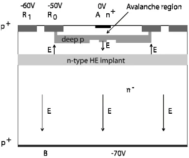
The concept of the avalanche drift diode is sketched in Fig. 1, showing a cross section through the inner part of a cylindrical device. This structure can be considered as the result of combining the drift diode [6, 7] with an avalanche structure directly underneath the electron collecting anode (A). The drift diode consists of p+ doped drift rings (R0, R1, …) and an n+ doped anode on one surface and a homogeneously p doped radiation entrance window on the opposite surface of the fully depleted silicon substrate.
Adding a buried p doped layer (deep p) underneath the anode (A) will generate a high field (avalanche) region above
Manuscript received October 30, 2004. Corresponding Author: Gerhard Lutz, e-mail:gel@hll.mpg.de. All authors at the MPI-Semiconductor Laboratory, Otto Hahn Ring 6, D81739 München, Germany
it if it is fully depleted. Full depletion can be accomplished by raising the voltage difference between anode and innermost drift ring (R0). Here it should be noticed that the field strength is determined by the deep p doping density and can be modified by a further increase of the innermost ring voltage while the influence of the backside voltage is almost non existent. The influence of the ring voltage on the field strength can be further increased by adding an additional ring-like buried p type doping, thus bringing the ring potential even closer to the avalanche region. This in addition improves focusing of signal electrons into the center high field region.
Additional deep p enhancement in the centre provides homogeneity of the high field region. This structure already shows the desired properties in simulations, however, there remains a low field region in the center beneath the avalanche region and careful adjustment of doping densities and operation conditions are required in order to assure full depletion of this region while simultaneously avoiding hole currents flowing from the drift ring towards the backside. This situation can be cured by an additional high energy n-type implant which assures a potential maximum in the drift region of the device while in and below the avalanche region the electric field does not change sign.
The Avalanche Drift Diode: A New Detector Concept for Single Photon Detection
Gerhard Lutz, Nepomuk Otte, Rainer H. Richter, Lothar Strüder
T
Fig. 1. Concept of the avalanche drift diode
III. SIMULATION:ELECTRIC FIELD CONFIGURATION
Device simulations have been performed for a structure as shown in Fig. 1 with 35µm radius and 50µm wafer thickness using the program package TeSCA [8,9]. This program simultaneously solves Poisson and continuity equations for electrons and holes. Charge generation processes including
avalanche generation are also modeled. Fig. 2 shows an isoline presentation of the potential distribution under typical operation conditions. One notices that electrons will initially drift approximately vertical towards a depth of 8 to 10 µm and then horizontally towards the centre where they turn downwards into the high field avalanche region.
The uniformity of the high field region is seen in Fig. 3 where a close-up view of the electric field magnitude around the anode is shown.
IV. SIMULATION:CHARGE FOCUSING PROPERTIES
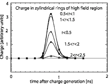
In order to function properly, nearly all electrons produced anywhere in the device have to reach the high field avalanche region. As a test we have simulated the production of an
Fig. 3. Isoline presentation of the simulated electric field strength in the small avalanche region situated at the lower left corner of Fig.2. The nearly uniform high field region extends to more than 2 µm radius
Fig. 2. Simulated potential distribution in the cylindrically symmetric avalanche drift diode shown in Fig. 1. One half of the device (r=0 to 35µm) is presented, with the anode located at the left lower corner
Fig. 5: Same as Fig. 4 but for generation at the edge of the simulation region (r=35µm)
Fig. 4. Arrival time and spatial distribution in the high field region of a point charge produced at the center of the entrance window. Avalanche multiplication was switched off in the simulation
electron hole pair near the entrance window, once in the centre (r=0) and once at the cell boundary (r=35µm). We have also divided the avalanche region into rings of 0.5µm width and looked at the electron charge in these cylindrical rings as function of time after generation. Notice that the simulation tool is unaware of granulation of electric charge and that the avalanche mechanism was turned off for this investigation.
Fig. 4 presents the result for generation at the centre and Fig.5 for generation at the fringe. The charge indeed is focused to the high field region in both extreme cases, although its center is shifting with position of generation.
V. SIMULATION:RESPONSE TO SIGNALS
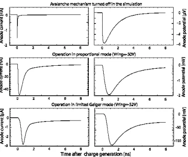
The response to single (optical) photons creating one electron hole pair and also to several electrons created simultaneously – as would be the case for X-rays – has been simulated. The anode A has been connected to ground potential by a capacitor of 10 fF in parallel with a resistor of 100 kΩ. These would be integrated into the device when used in limited Geiger mode.
We show the current, the quantity to be sensed in an amplifier connected to the device and the voltage at the anode which is a measure of the charge collected. Αs the program does not know the existence of the elementary charge, single simulated electrons would spatially disperse on their way towards the avalanche region. For that reason, in the simulation, the primary charge has been produced in immediate vicinity of the avalanche region.
The signal response has been investigated as a function of the biasing condition, varying the voltage difference between anode A and innermost drift ring R0.
Fig. 6 shows the response to a single electron entering the avalanche region. For three conditions: (i) the avalanche mechanism turned off for reference; (ii) at voltage difference of 50V resulting in proportional mode operation and (iii) at 52V resulting in Geiger mode operation.
The amplification factor of 330 in proportional mode for the conditions chosen was found by comparing the maximum voltage of the capacitor with the simulation in which the avalanche mechanism was turned off. Notice that part of the charge generated rests on the built in capacitance of the device which is of similar magnitude as the external capacitor.
The amplification for a single electron entering in the limited Geiger mode was estimated by the same method as 20000.
It has also been verified that in proportional mode the response of the device is indeed proportional to the number of electrons entering simultaneously the avalanche region while in Geiger mode the signal is independent on it.
VI. VARIATION OF DEVICE CONFIGURATION AND OPERATING
CONDITIONS
The simulation results shown above are for a single particular device configuration and also for a special operation mode with a load at the anode consisting of a small capacitor and a resistor in parallel. Increasing the capacitor in limited Geiger mode will increase charge amplification and duration of the voltage pulse. Increasing the resistance value will also increase pulse duration and in addition decrease the tail of the anode current pulse. Thus, quenching of the avalanche process (which is reached when the number of mobile carriers in the avalanche region fluctuates to zero) is facilitated.
Fig. 7 shows the result of a simulation with the capacitance increased by a factor five and the resistor increased by a factor ten. The device is in addition operated at higher anode-ring voltage difference. A very long voltage pulse is obtained, however, the current pulse remains short and its tail drops to very low value. Here it is interesting to note that the first part of the tail, which extends to approximately 5ns, is at least partially due to induction by the hole cloud which moves relatively slowly away from the avalanche region. This hole cloud seems also to play a role in limiting the avalanche as it contributes to a decrease of the electric field in the small (“point like”) avalanche region.
Fig. 6. Response to single electrons entering the avalanche region. Current and voltage at the anode are shown for the device connected by a resistor (100 kΩ) and a capacitance (10 fF) in parallel to an amplifier with its input at virtual ground.
Fig. 7. Response to single electrons in limited Geiger mode for a load of 1MΩ in parallel to a capacitor of 50 fF.
It should further be noted that the field configuration can be tailored to the requirements of the intended application. Very good time resolution, for example, limits the lateral dimension of the device since drift time differences enter directly into this property. There it is also preferable to choose a field configuration in which the primary electron takes an inclined path towards the avalanche region. Further investigations underway concern the vertical extent of the avalanche region.
Furthermore the high energy implant may be varied in depth and can also be structured.
VII. CONCLUSIONS
Our new concept of the avalanche drift diode structure promises high photon detection efficiency over the full energy range of optical photons. This is due to placing the thin homogeneous entrance window on the backside of a fully depleted silicon substrate and the focusing of the electrons generated by radiation onto a small (point-like) avalanche region. The latter is accomplished with the help of a drift diode structure.
The new structure can be used as building block for a “Silicon Photomultiplier Tube” (SiPMT)
Extended simulations have shown the validity of the concept.
Layout of the new structures is starting. They will be produced in our laboratory within its complete planar silicon detector
processing line. As a first step simple test structures will be produced that will allow verification of the parameters which entered into the device simulations. This will be followed by production of complete avalanche drift detector structures and small size SiPMTs.
VIII. REFERENCES
[1] M. Teshima, et al., “EUSO (The Extreme Universe Space Observatory)- Scientific Objectives”, Proceedings ICRC 2003, pp. 1069
[2] J. A. Barrio, et al., “Design report on MAGIC”, MPI-PhE/98-5 (March 1998)
[3] V. Golovin and V. Sveliev. Novel type of avalanche photodetector with Geiger mode operation”, NIM A 518 (2004), p. 560-564
[4] B. Dolgoshein, et al., “Silicon photomultiplier and its possible applications”, NIM A 504 (2003), p. 48-52
[5] D. Bisello, et al., NIM A 367 (1995) pp. 212
[6] J. Kemmer and G. Lutz: ''New semiconductor detector concepts'', Nucl.
Instr. & Meth. A 253 (1987) 365-377
[7] J.Kemmer, G. Lutz et al., "Low capacitive drift diode", NIM A253 (1987) 378-381
[8] H. Gajewski et al., "TeSCA – Two Dimensional Semiconductor Analysis Package", Handbuch, Weierstraß -Institute for Applied Analysis and Stochastics WIAS, Berlin, 1997
[9] H. Gajewski, H.-Chr. Kaiser, H. Langmach, R. Nürnberg and R. H.
Richter: "Mathematical Modeling and Numerical Simulation of Semiconductor Detectors", Springer-Verlag, Berlin (2001)
Fig. 5: Same as Fig. 4 but for generation at the edge of the simulation region (r=35µm)
Fig. 4. Arrival time and spatial distribution in the high field region of a point charge produced at the center of the entrance window. Avalanche multiplication was switched off in the simulation