Study of noise and spectroscopic performance of DEPMOSFET matrix prototypes for XEUS
J. Treis
a,∗ , P. Fischer
b, O. H¨ alker
a, M. Harter
b, S. Herrmann
a, R. Kohrs
c, H. Kr¨ uger
c, P. Lechner
d, G. Lutz
e, I. Peric
b, M. Porro
f, R. H. Richter
e, L. Str¨ uder
a, M. Trimpl
cand
N. Wermes
caMPI f¨ur extraterrestrische Physik, Giessenbachstrasse, 85748 Garching, Germany
bMannheim University, Institut f¨ur technische Informatik, D7 2-4, 68159 Mannheim, Germany
cPhysikalisches Institut der Universit¨at Bonn, Nußallee 12, 53112 Bonn, Germany
dPNSensor GmbH, R¨omerstraße 28, 80803, Munich, Germany
eMPI f¨ur Physik, F¨ohringer Ring 6, 80805 Munich, Germany
fPolitecnico di Milano, Dipartimento di Elettronica e Informazione, Via Golgi 40, 20133 Milano, Italy
Abstract
The current generation of DEPMOSFET based Active Pixel Sensor (APS) matrix devices has been developed to cope with the challenging requirements of the XEUS Wide Field Imager. The devices turned out to be a promising new imager concept for a variety of X-ray imaging applications. The devices combine excellent energy resolution, high speed readout and low power consumption with the attractive feature of random accessibility of pixels. Sensor prototypes, built for row-wise readout, with 64 x 64 pixels with a size of 75 x 75µm2 each have been produced at the MPI semiconductor laboratory in Munich, and their performance has been studied in detail. A spectroscopic resolution of 128 eV has been measured, the readout noise is as low as 3.5 e−ENC. Here, measurements of the dependence of readout noise and spectroscopic resolution on the device temperature are presented.
Key words: XEUS, DEPFET, X-ray, astronomy, Imaging, Spectroscopy, Active Pixel Sensor PACS:95.99.Ka, 07.85.Fv, 07.85.Nc
1. Introduction
DEPFET APS based sensors of the current gen- eration turned out to be a promising new con- cept for both imaging applications and high res- olution spectroscopy. As with the latest advance- ments of technology [1] large-area APS sensors us-
∗ Corresponding author. Tel. +49 89 83940045, fax. +49 89 83940013, e-mail jft@hll.mpg.de
ing DEPFETs come within reach, a design concept for the Wide Field Imager (WFI) [2,3] of the X- ray Evolving Universe Spectroscopy (XEUS) [4,5]
mission was proposed, which includes a large area DEPFET array. At the present stage, the device will have a total area of 76.8 mm×76.8 mm, di- vided into 1024×1024 pixels of 75µm ×75µm size each [6].
A production of DEPFET sensors including sensor prototypes for XEUS has recently been finished at
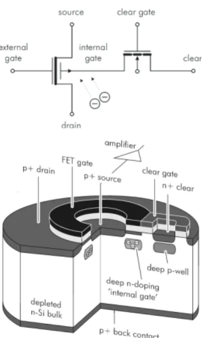
Fig. 1. Cutaway and circuit schematic of a circular DEP- MOSFET pixel. A pixel consists of a circular p-channel MOSFET with attached clear region, forming an addi- tional ’parasitic’ n-channel MOSFET contacting the inter- nal gate.
the MPI semiconductor laboratory in Munich. The new devices use MOSFETs as amplifying transis- tors instead of the JFETs used in earlier devices, as better homogeneity and reproducibility can be provided in this way.
Results on measurements on DEPMOSFET struc- tures presented elsewhere [6,7] have proven the suitability of DEPMOSFET based devices for the advanced requirements of the XEUS experiment.
Here, measurements on noise and spectroscopic performance are presented.
2. DEPMOSFET devices
A DEPMOSFET (DEpleted P-channel MOS- FET) consists of a p-channel MOS-field effect transistor integrated on the surface of a high re- sistivity n-type silicon bulk. The bulk is fully depleted making use of the principle of sideways depletion [8]. The potential minimum for electrons thus generated is confined further in lateral direc-
Fig. 2. Microscope photography of a DEPMOSFET struc- ture. The circular polysilicon gate has a width of 5µm and a circumference of 47.5µm. The bright horizontal lines are the metal connections of drain, gate, clear and cleargate.
The source is connected in vertical direction by the curved polysilicon gates.
Fig. 3. Simplified interconnection scheme of pixels on the DEPMOSFET matrix protoypes for XEUS. All pixels have a common drain contact. The gates, cleargates and clear contacts are connected row-wise, while the pixel sources are connected column-wise. Every source column is biased by a column-individual current source, which is provided externally.
tion to the area below the transistor channel by an additional n-doped region, which also increases the depth of the potential minimum. Electron-hole pairs generated in the silicon bulk are separated by the electric field and the electrons are collected in the potential minimum below the transistor
channel, modifying the charge carrier density in the channel by inducing an additional amount of holes. Thus, the channel conductivity is a function of the amount of charge in the potential minimum, which is therefore calledinternal gate.
The internal gate is capable of storing signal charges regardless of the presence of a transistor current, so the transistor current can be turned off during signal integration. This reduces power consumption. To prevent the charge storage capa- bility from getting lost due to an completely filled internal gate, the accumulated charge has to be removed regularly by applying a positive voltage pulse to the so-calledclear-contact, an n+-doped region close to the internal gate.
For the sake of improved charge collection and a more efficient filling of the pixel area, the DEP- MOSFET structures designed as prototypes for the XEUS WFI have circular transistor geometry.
Theclear regionhere consists of the clear contact and a surrounding MOS structure, the so-called cleargate, which forms a tunable barrier between clear contact and internal gate. An additional deep p-implanted well underneath the clear, the so-calleddeep p, provides further separation of the clear contact from bulk and internal gate. Clear and cleargate together can be considered as a par- asitic n-channel MOSFET connecting clear and internal gate. Figure 1 shows a cutaway of a cir- cular DEPMOSFET structure. A photo of a fully processed DEPMOSFET pixel device surface can be seen in figure 2.
The DEPMOSFET structures for XEUS have been designed for source follower readout. Here, the pixel source contact is biased by a constant current source and a change in the MOSFET channel conductivity yields a voltage step at the source node proportional to the amount of charge collected. As the complete clear provides for a re- producible baseline, comparing the voltage levels at the source node of the pixel before and after the clear process provides the signal information. In the first, simplified approach, the relation between the charge in the internal gate and the resulting voltage step at the source node can be calculated by assuming a DEPMOSFET transistor in satu- ration and the load current to be constant. In the small signal case, the overall change in transistor
current is thus given by
δi = gm ·δvGS + gD · δvDS + gq · ∆Q, where gm is the transconductance of the DEP- MOSFET’s external gate,gq the so-calledcharge transconductance, which is the ratio
gq = δIpixel
δqint. gate
, (1)
and ∆Qsthe change in the amount of signal charge in the internal gate, either removed from the inter- nal gate during the clear process or accumulated during the integration period. Due to the constant current bias,
0 = δi = gm · (δvG−δvS) + gD · (δvD−δvS) + gq · ∆Q,
which, assumingδvD = 0, can be simplified to δvS · (gm+gD) = gm · δvG + gq · ∆Q, which, usingδvG = 0 and neglecting the output resistancegD ≈ 0, yields
∆Vs = gq
gm ·∆Qs.
A more sophisticated model of the DEPMOSFET source follower as a dual gate follower including also noise considerations is given in [9].
For building large area sensors with DEPFET pix- els, a pixel array is integrated onto a single die with common bulk and back contact. By applying a suitable interconnection scheme between the in- dividual transistor terminals, groups of pixels can be formed and randomly accessed. For the current DEPMOSFET structure prototypes, a simple in- terconnection scheme has been chosen, which is shown in figure 3. All matrix pixel are connected to a common drain. Gate, clear and cleargate con- tacts are connected row-wise and the sources of all transistors within one pixel column are connected as well. For the source follower mode operation, every column is contacted by an external current source. By applying appropriate voltages to the gate contacts, only a single row of pixels can be turned on. Thus, voltage changes at the column- individual source node are due to changes of the
internal gate fill level of the pixel in the row which is currently active.
Matrix readout is done row-wise, i.e. the signal in- formation of all pixel in a row is processed in par- allel. All pixels integrate signal charges for a fixed time interval. For readout, the transistor currents in the respective row are turned on via the external gate voltage. The voltage level at the source node is measured. Next, the clear operation is performed in the row by using clear and cleargate contacts.
The voltage level at the source node now corre- sponds to the baseline information, the pixel sig- nal with empty internal gate. The charge informa- tion can be obtained from calculating the voltage difference before and after the clear, and the tran- sistor current in this row can be turned off. Then, the process is repeated in the next row. Thus, the minimum integration time for a row of matrix pix- els is given by the time needed to read out all other rows in the matrix.
The XEUS DEPMOSFET matrix prototypes con- sist of matrices of 64×64 pixels of 75 ×75 µm2 size. The device has a total sensitive area of 4.8
×4.8 mm2 and is integrated onto a 450µm thick bulk. For the most favored structures, the circu- lar transistor gate has by design a circumference of 47.5µm and a nominal gate width of 5µm. The drain contact is in the center of the pixel. The inter- nal gate geometric size and doping concentration are dimensioned to store more than 105electrons in a pixel, and measurements show that no deviation from linearity is observed up to that limit. For the current structures,gq-values of≈200 - 300 pA / e−have been measured, depending on parameters like implantation profile, effective channel length and operating conditions. However, as the DEP- MOSFET follower is not a pure source follower, the figure of merit for the source follower configuration is thecharge conversion gainof the source follower gs = gq
gm
(2) expressed inµV signal step per e−charge stored in the internal gate. For the current structures, val- ues of 3.7 - 4.8µV / e−have been measured.
The matrix device, whose measurements are pre- sented here, is not uniform. The left half of the matrix is equipped with so called P1 pixels, which
Fig. 4. Left: Close-up of the central area of a hybrid, with the sensor (middle), the Clear switcher (right), the Gate switcher (left) and the CAMEX IC at the lower edge of the sensor. The wire bond interconnections between the different ICs are visible. Right: Overview over a PCB type hybrid with the connector pins to the peripheral readout electronics and a coin showing the proportions.
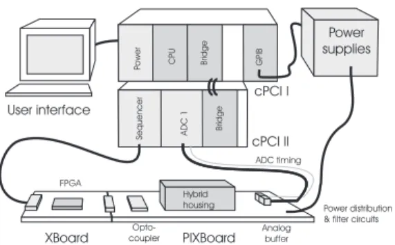
Fig. 5. Simplified schematic of the system setup. A cPCI CPU controls the sequencer card and the DAQ ADC card.
The control sequence is transferred via the XBoard to the PIXBoard, which holds the hybrid and performs galvanic decoupling, level shifting, bias generation and distribution and filtering for the required operation voltages. The analog output signals of the hybrids are transferred to the ADC card, which digitizes and formats the data.
have a relative large overlap between the deep-p shielding the clear and the cleargate (see figure 1), while the right half of the matrix has the P0 option pixels, for which the overlap is reduced to the small- est extend possible. P0 pixels are less demanding in terms of clear resources, i.e. time and voltage, while P1 pixels provide better shielding of the clear and thus improved protection against charge loss to the clear. A more detailed description of the different design variants and their implications on device performance can be found in [10].
3. DEPMOSFET readout
The matrix devices are integrated together with the required front end ICs and additional filter circuitry onto a hybrid carrier. Figure 4 shows photographs of a fully assembled readout hybrids.
A more detailed description of the front-end elec- tronics can be found in [11].
For switching the gate, cleargate and clear volt- ages, the SWITCHER II IC is used, which is a 64 channel, dual output, high voltage switching cir- cuit manufactured in an AMS high voltage CMOS process. Having been designed for the purpose of DEPMOSFET matrix readout, it provides two output ports for every channel, which can be tog- gled between two individual voltages each, facili- ties for precise timing of the switching process and easy integration of a number of SWITCHER ICs to a daisy chain in case large sensor arrays have to be read out. The total switch voltage difference can be as large as 20 V.
The analog front end IC is the so-called CAMEX 64 G, which is a 64 channel parallel voltage am- plifier with an 8 fold correlated double sampling (CDS) stage and serial analog readout. It is a vari- ant of the CAMEX family [12], which has been adapted to the requirements of DEPMOSFET pixel readout. It has a PMOS current source in- tegrated in every channel for biasing of the pixel columns. Typical operation currents are about 20 µA. Additionally, a built-in sequencer allows very flexible signal shaping schemes. The analog signal voltage information is read out using a sample &
hold in combination with a serializer circuit. A publication containing a detailed discussion of the CDS filter properties of the CAMEX CDS filter and the influence of sample timing and amplifier bandwidth on the filter efficiency is currently in preparation.
Figure 5 shows a simplified schematic overview over the peripheral readout system. A more de- tailed description can be found in [11]. All digital signals required by the readout system are gen- erated by a commercially available cPCI pattern generator, which also permits access to the sys- tem’s slow control interface.
The XBoard (XILINX-Board), an FPGA based
multi-purpose digital interface card, was added to the setup to overcome certain limitations of the sequencer card and to increase flexibility in read- out timing. In addition, it allows for very flexible matrix control, permitting, for instance, precise clear and timing measurements on single pixels within a matrix.
The so-called PIXBoard (PIXel Board) decouples the inner circuits of the setup galvanically from XBoard and sequencer card and holds the readout hybrids within an electrically shielded, light-tight housing. In addition, it provides digital and ana- log driver circuitry and all supply and bias for the readout hybrid.
The ADC board consists of a cPCI base board equipped with a custom made 14-bit ADC piggy back. An effective ADC resolution of 11.7 bit can be achieved with this system. A number of format signals allow for storage of data in a frame- compatible format. The system can cope with a data rate of 40 MByte/s. A cPCI-GPIB interface permits control of the system power supplies and calibration facilities. The system is modular and scalable, so it can grow with increasing sensor sizes.
4. Measurement results
As this has been the first sensor prototype pro- duction, many different pixel variants have been produced, the most promising of which have in the meantime been determined. The measure- ments presented in the following were made on the structure type which turned out to show the best performance. The device was illuminated with an 55Fe source while being operated in a dried air atmosphere within a climate chamber at tem- peratures between +20◦C and -60◦C. the device was illuminated from both front- and backside to study the effect of different widening of the charge cloud on the energy resolution.
As for the measurements presented here speed was not an issue, the device was read out at a relatively low frame rate of about 300 Hz, which leaves each pixel with a signal and leakage current integration time of about 3 ms. Hereby, the time
-60 -40 -20 0 20 1
10
PixelLeakagecurrentnoise(e-ENC)
Temperature (°C)
-60 -40 -20 0 20
10 20 30 40 50 60 70
2.78 5.56 8.33 11.11 13.89 16.67 19.44
Normal cycles (tInt= 3 ms) Reference cycles (tInt= 5?s)
Pixelreadoutnoise(e-ENC)
Pixelreadoutnoise(eV)
Temperature (°C)
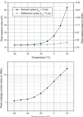
Fig. 6. Dependence of total pixel noise (normal cycles) and readout noise (reference cycles) on device temperature (up- per plot). The total noise of a pixel corresponds to the standard deviation of the offset values of that pixel mea- sured during the dark period. The readout noise is mea- sured in the same way, but with an additional clear remov- ing most of the influence from integrated leakage current.
Subtracting readout from total noise quadratically yields the leakage current contribution to the total noise (lower plot), which shows an exponential temperature dependence up to -20◦C.
used to actually perform the acquisition of the analog data within one pixel row was about 25µs.
The matrix pixels were operated at a pixel current of 25µA, which provides for a mean pixel charge conversion gain of 4.2µV / e−.
4.1. Signal considerations
For data analysis, a number of≈500 so-called dark framesare taken, when no radioactive source is present. Right afterwards, the source is posi- tioned above or below the device and a number of ≈ 35000 illuminated frames is taken. The off-
set map for the device is determined by calculating the mean signal voltage for the dark frames. The total noiseof the individual pixels is given by the standard deviation of the respective offset values.
It consists of a channel-individual offset value gen- erated by the CAMEX channel and the integrated leakage current charge of the respective pixel.
Looking at the illuminated frames, event identifica- tion is done on the basis of a pixel individual event threshold, which is determined by the pixel noise.
A primary photon event is identified, if a pixel sig- nal exceeds its offset by more than 5σ, withσbe- ing the pixel noise. In case of composite patterns due to charge sharing, pattern constituents are de- tected next to a primary event above a threshold of 2.5σ.
At present, the pixel data is calibrated by assum- ing an ideal linear gain for both CAMEX and pixel, but assuming different gain values for the individ- ual pixels.
This gain map is calculated by determining the peak position of the55Mn-Kα-peak for every single pixel using only non-composite patterns (singles), where no charge sharing occurs. The gain disper- sion, i.e. the gain spread over the matrix, is below 5%. The signal acquired from a pixel (i,j) is com- posed from 3 contributions
Vs = VO(j) + g(j)C · g(i,j)s · (q(i,j)lk +q(i,j)sg ) (3)
whereVO(j)is the column-individual CAMEX offset voltage,g(j)C the column-individual CAMEX gain, g(i,j)s the pixel-individual charge conversion gain as given by equation 2, qlk(i,j) the pixel-individual leakage current charge accumulated during the in- tegration period andq(i,j)sg the real signal charge, which is of course only present in case event charge was collected by the pixel.
Using the gain map, the pixel data can be cali- brated and the energy spectra can be calculated by recombining composite patterns. To determine the spectral energy resolution of the device, the figure of merit is the FWHM of the55Fe-Kα-peak for the singles spectrum.
-40 -30 -20 -10 0 10 20 0.1
1 10
Pixelleakagecurrent(fA)
Temperature (°C)
10 20 30 40 50 60
10 20 30 40 50 60
Column #
Row#
13.00
17.00
21.00
25.00 Pixel leakage current @ 20 °C (fA)
10 12 14 16 18 20 22 24 26 28 30
1 10 100
Pixelcount
Pixel leakage currentv (fA)
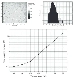
Fig. 7. Temperature dependence of pixel leakage current (lower plot). As expected, the leakage current shows an ex- ponential dependence on temperature down to a tempera- ture of -20◦C. Below that limit, measurement accuracy is limited by the intrinsic noise of the readout system. The overall distribution of leakage current at 20◦C (upper row) shows a mean value of 16.5 fA / pixel, a leakage current dispersion of 1 fA and a quite homogeneous spatial distri- bution with a slightly higher leakage current at the device borders.
4.2. Noise measurements
The device noise is composed of contributions from readout system and front end electronics, of the DEPMOSFET detector itself and noise con- tributions due to leakage current. These contribu- tions can be measured individually as a function of temperature.
As the total noise is determined from the dark frames, both signal processing electronics and leakage current integration contribute to the to- tal noise. In case, however, an additional clear is applied right before the sampling of the current source voltage level begins, the leakage current can be suppressed by a factor corresponding to the quotient of readout and integration time:
Vs = VO(j) +
gC(j) · gs(i,j) · ηtq(i,j)lk
with ηt = 1 for normal integration and ηt <
tro/ tint for the reference measurement. Thus, its contribution to the noise reduces accordingly. In our case,ηt ≈ 0.013.
By subtracting thereadout noisemeasured in this way quadratically from the total noise, the frac- tion of the total noise caused by solely the leakage current can be extracted. Figure 6 shows the tem- perature dependence of the different fractions.
The device noise behaves as expected. The read- out noise of the device at room temperature is as low as 4.7 e− ENC, which is in good agreement with the result predicted by applying the mea- sured CAMEX filter function to the measured noise power spectrum of a DEPMOSFET pixel at room temperature [9]. With decreasing tempera- ture the noise also decreases to a level of 3.5 e− ENC due to the decrease of series noise within the pixel MOSFET and the CAMEX, and also the remaining small leakage current contribution re- duces. As expected, the measured leakage current contribution itself shows an exponential behavior down to a temperature of -20◦C, where the read- out noise becomes dominant.
4.3. Leakage current
Using the reference frames with an additional clear in advance, the pixel leakage current can be measured directly. Subtracting equation 3 for dark frames and reference frames yields
∆Vs = gC(j) · gs(i,j) · (1 − ηt) · qlk(i,j)
Thus, subtracting the dark reference offset map from the dark signal offset map and dividing by the gain map yields the accumulated charge dur- ing integration period, which can be used to calcu- late the pixel individual leakage current. As shown in figure 7, the leakage current shows the expected exponential behavior down to a temperature of - 20◦C, below which the measurement is limited by the intrinsic readout noise of the front end chain.
At room temperature, a mean pixel current of 16.5 fA / pixel is measured, corresponding to a current of 285 pA / cm2. The leakage current dispersion is about 1 fA, and the corresponding leakage cur-
0 1000 2000 3000 4000 5000 6000 7000 1
10 100 1000
Counts
Energy (eV) 20 °C
0 1000 2000 3000 4000 5000 6000 7000
1 10 100
Counts
Energy (eV) 20 °C
0 1000 2000 3000 4000 5000 6000 7000
1 10 100 1000
-60 °C
Counts
Energy (eV)
0 2000 4000 6000
1 10
100 -60 °C
Counts
Energy (eV)
Fig. 8. Examples for energy spectra for frontside (upper row) and backside (lower row) illumination taken at room temperature (left column) and -60◦C (right column). The frontside illuminated spectra show a much worse peak / background ratio due to the influence of the dead layers on the electronics side. The prominent low energy background is not consistent with the noise peak.
rent map shows a homogeneous distribution with slightly higher values at the borders of the pixel area and few odd pixels. Previous measurements on diodes estimated the bulk leakage current of the devices to be about 200 pA / cm2, which is in good agreement with the new numbers taking into account the additional contributions from surface leakage current.
4.4. Spectral resolution
The spectral resolution of the devices is calcu- lated by determining the width of the 55Mn-Kα- peak in the singles spectrum for the given temper- ature. Figure 8 shows some examples for fit spec- tra taken at room temperature (left column) and -60◦C (right column) for frontside (upper row) and backside (lower row) illumination.
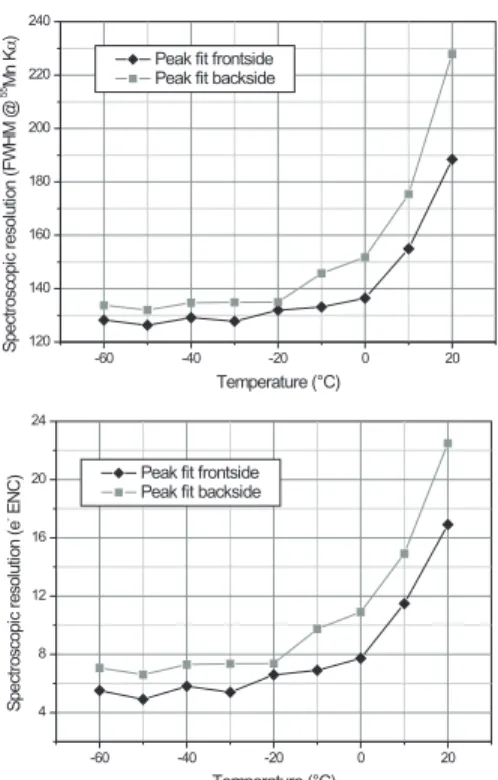
All spectra look very good; All spectral features are clearly visible. The measured spectral resolu- tion is 16.5 e− (frontside) and 22.5 e− (backside) for room temperature or 5.5 e−(frontside) and 7.0 e− (backside) respectively for the cold tempera- ture. The spectra for backside illumination show a much better peak to background ratio, as the back- ground for frontside illumination is dominated by partials caused by the dead layers on top. However,
-60 -40 -20 0 20
120 140 160 180 200 220 240
Peak fit frontside Peak fit backside
Spectroscopicresolution(FWHM@55MnK?)
Temperature (°C)
-60 -40 -20 0 20
4 8 12 16 20 24
Peak fit frontside Peak fit backside
Spectroscopicresolution(e-ENC)
Temperature (°C)
Fig. 9. Dependence of measured spectral resolution at the
55Mn-Kα-peak on the device temperature. Given are the values in eV FWHM (upper plot) and in e− ENC after subtraction of the Fano noise contribution (lower plot). Not much change is seen below -20◦C. The energy resolution becomes as good as 4.9 e− for frontside illumination and 6.6 e−for backside illumination.
due to the large thickness of the device, the frac- tion of singles reduces and collecting a sufficient number of singles for gain determination becomes thus difficult. As the operating conditions remain unchanged, it is justified to apply the gain map from the frontside illumination for the calibration of the backside illuminated measurement.
Figure 9 shows the dependence of the spectral en- ergy resolution on the device temperature. As ex- pected, the spectral resolution improves with de- creasing temperature as the total noise decreases and saturates at approximately the same tempera- ture as the total noise does. The energy resolution becomes as good as 4.9 e− ENC for the frontside illumination and 6.6 e− ENC for the backside illu- mination.
0 10 20 30 40 50 60 70 80 90 100 0.1
1 10 100 1000
#Pixels
# Correlation events
10 20 30 40 50 60
10 20 30 40 50 60
Column #
Row#
3.000
9.182
28.10 86.00 Number of clear correlations per pixel (logarithmic scale)
P1 P0
Frame #N+1 (successor pattern)
Frame #N (precursor patttern)
Frame #N+2 (successor pattern
2nd order)
Fig. 10. Principle of clear correlations (left), correlation map (upper right) and frequency distribution (lower right).
Most of the correlating pixels show up in the P1 half due to unfavorable clear conditions and show a small number of correlations. Fewer pixels showing a large number of correlations are distributed all over the device.
The discrepancy between the spectral resolution and the total noise can be explained taking into account effects like incomplete charge collection, sub-threshold charge loss to neighboring pixels and possible CAMEX nonlinearities, but as the data analysis is at a relatively early stage, these effects which will be studied more in detail later.
Also not fully understood is the large discrepancy between the energy resolution measured for the frontside and the backside illumination. Possible explanations are differences in charge collection between front- and backside illumination, which might influence the determination of gain, thresh- old effects or analysis artifacts. A more detailed study of charge collection will clarify this question.
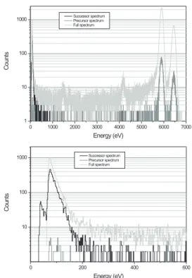
4.5. Low energy background
A common feature of the spectra shown in figure 8 is the prominent low energy background, which is not consistent with pixel noise and threshold. For the given settings, the background due to device noise is expected to be about a factor of 70 lower.
0 1000 2000 3000 4000 5000 6000 7000
1 10 100
1000 Successor spectrum
Precursor spectrum Full spectrum
Counts
Energy (eV)
0 200 400 600
10 100
1000 Successor spectrum
Precursor spectrum Full spectrum
Counts
Energy (eV)
Fig. 11. Full range correlation spectra (upper plot) and close-up in the low energy range (lower plot). It can be seen, that the successor spectrum almost perfectly describes the shape of the low energy background of the overall spectrum.
This anomalous low energy background turns out to be due to pixels, which do not have the complete charge removed with one clear, so the remaining charge is detected at the same position in the sub- sequent frame. Thus, consecutive frames can show events in the same pixel, the first in the 55Mn- Kα-region, and the second one in the low energy background region. For a few pixels, even correla- tions over 3 subsequent frames have been found.
The majority of these low energy events contains amounts of charges of≈50 e− and below.
The effect has been studied in detail. It turned out that the occurrence of these clear correlations is not due to conceptual problems achieving a com- plete clear, but due to insufficient clear conditions and clear inhomogeneity. Figure 10 shows the dis- tribution and frequency of occurrence of the clear correlations for the measurement taken at -60◦C.
It can be seen that most of the pixels showing clear
correlations show a small number of correlation occurrences compared to the 35000 frames taken.
They are located in the P1 half of the matrix and see unfavorable clear conditions. This fraction de- creases strongly in case higher clear voltages are applied or the clear time is slightly increased.
The remaining small fraction of pixels shows a larger number of correlations. They show up in both P1 and P0 half of the matrix. Only these pix- els also occasionally show higher order clear corre- lations. For these pixels, imperfections in the circu- lar gate geometry caused by lithography problems which were solved in the meantime give raise to small potential barriers inside the internal gate it- self. To overcome these potential barriers, charges in the internal gate have to emit thermally over the barrier, which is time consuming and temperature depending, and which causes the observed correla- tion behavior.
It can be seen from figure 11, that the correlation spectrum taken only from singles almost perfectly describes the low energy background. For future productions, the problem will be avoided by ap- plying the P0 or a P0 like deep-p overlap to all de- vice pixels, by ensuring perfectly circularly shaped external gates and by introducing a second clear contact opposite the clear contact shown in figure 1. This second clear contact will eliminate the dif- fusion component from the clear behavior and in- crease the speed of the clear process drastically.
5. Conclusions
DEPMOSFET based X-ray detector prototypes for XEUS have been characterized with respect to readout noise and spectroscopic resolution. The re- sults are very promising. The readout noise has been determined to be as low as 3.5 e− ENC, a spectroscopic resolution of 128 eV FWHM (5.5 e− ENC) at55Mn-K-α(133 eV (7 e−ENC) for back- side illumination) has been measured.
Even at room temperature, the detectors show an acceptable performance with a total noise of 17− and an energy resolution of 190 eV (17 e− ENC) at the frontside and 230 eV (22 e− ENC) at the backside. The anomalous low energy background
has been studied and traced back to unfavorable clear conditions and imperfect pixels, so they can be avoided for future large area devices.
In the near future, the charge collection of the devices will be studied using a variety of tech- niques, e.g. laser scanning or measurements using the mesh methods, to understand the limitations on the spectroscopic resolution with respect to the device noise. Especially the different behavior of front- and backside illumination are of concern. Im- proved algorithms will help to suppress systematic errors introduced by the analysis, and simulations are in progress to study the charge spread and col- lection within the device in detail to improve the performance for future devices.
References
[1] R. Richter et al., Design and technology of DEPFET pixel sensors for linear collider applications, Nucl.
Instr. and Meth. A 361 (2003) 250.
[2] X-ray Evolving Universe Spectroscopy-The XEUS Telescope, The XEUS Telescope Working Group, ESA SP-1253,ftp://www.rssd.esa.int/pub/XEUS/
BROCHURE/sp1253A.pdf, 2001.
[3] X-ray Evolving Universe Spectroscopy-The XEUS Instruments, The XEUS Instrument Working Group, ESA SP-1273,ftp://www.rssd.esa.int/pub/XEUS/
BROCHURE/sp1273web.pdf, 2003.
[4] X-ray Evolving Universe Spectroscopy-The XEUS Science case, The XEUS Astrophysics Working Group, ESA SP-1238, ftp://www.rssd.esa.int/pub/XEUS/
BROCHURE/brochure.pdf, 2000.
[5] X-ray Evolving Universe Spectroscopy-The XEUS Mission Summary, The XEUS Steering Commitee, ESA SP-1242, ftp://www.rssd.esa.int/pub/XEUS/
BROCHURE/sp1242.pdf, 2000.
[6] L. Strueder et al., XEUS wide-field imager: first experimental results with the X-ray active pixel sensor DEPFET, in: A. D. Holland (Ed.), High- Energy Detectors in Astronomy, Vol. 5501 of SPIE proceedings, 2003.
[7] P. Lechner et al., DEPFET integrated amplifiers for x-ray imaging and spectroscopy active pixel sensors, in: High-Energy Detectors in Astronomy, SPIE proceedings, 2004.
[8] E. Gatti, P. Rehak, Semiconductor drift chambers-an application of a novel charge transport scheme, Nucl.
Instr. and Meth. A 225 (1984) 608.
[9] M. Porro et al., Spectroscopic performances of DePMOS detector/amplifier device with respect to different filtering techniques and operating conditions, Paper accepted by IEEE Transactions on Nuclear Science.
[10] J. Treis et al., DEPMOSFET Active Pixel Sensor Prototypes for the XEUS Wide Field Imager, IEEE Transactions on Nuclear Science 52 (2005) 1083 – 1091.
[11] J. Treis et al., First results of DEPFET based Active Pixel Sensor prototypes for the XEUS Wide Field Imager, in: A. D. Holland (Ed.), High- Energy Detectors in Astronomy, Vol. 5501 of SPIE proceedings, 2004, pp. 89–100.
[12] W. Buttler, G. Lutz, V. Liberali, F. Maloberti, P. Manfredi, V. Re, V. Speziali, Evolution in the criteria that underlie the design of a monolithic preamplifier system for microstrip detectors, Nucl.
Instr. and Meth. A 288 (1997) 140.