Current and noise properties of interacting nanojunctions
Dissertation zur Erlangung des Doktorgrades der Naturwissenschaften (Dr. rer. nat.) der Fakultät für
Physik der Universität Regensburg
vorgelegt von Michael Niklas aus Deggendorf
im Jahr 2018
Termin Promotionskolloquium: 27.04.2018 Prüfungsausschuss:
Vorsitzender: Prof. Dr. Christoph Strunk Erstgutachter: Prof. Dr. Milena Grifoni Zweitgutachter: Dr. Sigmund Kohler Weiterer Prüfer: PD Dr. Falk Bruckmann
For science
i
Acknowledgements
At this point I would like to acknowledge everyone supporting me during my PhD and even making it possible in the first place.
First of all I would like to thank Milena Grifoni for introducing me into the field of condensed matter physics already during my Bachelor’s thesis. Its topics are still fascinating and challenging after so many years. Thank you very much for welcoming me in your group of wonderful people and guiding me patiently through all my problems. I really enjoyed working at your chair with its wonderful atmosphere.
A special thanks goes to Andrea Donarini for answering all my “5 minutes”
questions and helping me endless hours with models and numerics. Your insight and intuition in physics is what advanced large parts of the work.
Furthermore I want to thank Sigmund Kohler and his colleagues for teaching me the ways of full counting statistics during my stay in Madrid. I also enjoyed the after-work hours even though we will probably always stay opponents in football.
Thanks to all my colleagues in Regensburg: Magdalena Margańska, Paul Wenk, Ivan Dmitriev, Heng Wang, Michael Kammermeier, Felix Weiner, Matthias Stosiek, María Camarasa Gomez, Martin Wackerl, Patrick Grössing, Nico Leumer, Sebastian Pfaller, Sonja Predin, Sergey Smirnov, Benjamin Siegert, Davide Mantelli, Andreas Trottmann, Wataru Izumida and especially my two office mates Lars Milz and Daniel Hernangomez Perez.
I think our sysadmin group made a perfect team. A cheer to Felix Weiner, Raphael Kozlovsky, Josef Rammensee, Jacob Fuchs and Tobias Frank. May the cluster always run.
Without the help of Sylvia Hrdina, Claudia Zange and Robert Hrdina nobody can survive in the bureaucracy of the university, thank you.
My sincere thanks to the groups of Jean-Pierre Cleuziou from Grenoble and Christoph Strunk from Regensburg for providing our group with amazing
iii
experiments to analyze. In particular I would like to thank Ngoc-Viet Nguyen, Wolfgang Wernsdorfer, Michael Schafberger and Nicola Paradiso.
Financial support by the Deutsche Forschungsgemeinschaft via SFB 689 and GRK 1570 as well as by the Elitenetzwerk Bayern via their international doctorate program “Topological Insulators” is acknowledged.
In particular I want to thank my wonderful girlfriend Mónica for encouraging and pushing me the whole time. Without physics I would have never found you. I love you!
Last but not least a big thanks to my family. Thanks to my parents I could enjoy the education enabling me to study physics in the first place. Thank you for supporting me the whole time. A big thanks to my brother and sister for sweetening my weekends. Without you all I would not be where I am now.
Table of Contents
List of publications ix
Abstract xi
Introduction 1
I Transport across interacting carbon nanotube quantum
dots 7
1 Carbon nanotube quantum dots 9
1.1 The single-electron transistor . . . 10
1.1.1 Transport regimes . . . 10
1.1.2 Capacitor model of metallic islands . . . 11
1.1.3 Coulomb blockade . . . 12
1.1.4 Non-linear transport . . . 13
1.1.5 Excited states . . . 15
1.1.6 Co-tunneling . . . 17
1.2 Electronic properties of CNT-QDs . . . 18
1.2.1 Graphene . . . 19
1.2.2 Classification of carbon nanotubes . . . 20
1.2.3 Transverse quantization . . . 21
1.2.4 Low energy expansion . . . 23
1.2.5 Effects of curvature, magnetic fields and boundaries . . 24
1.2.6 Finite length carbon nanotubes . . . 26
1.2.7 Model Hamiltonian . . . 27
1.2.8 Exchange interaction . . . 28
1.2.9 Spectrum in a magnetic field . . . 29 v
2 Transport theory 33
2.1 Open quantum systems . . . 34
2.2 Quantum master equation . . . 35
2.2.1 Nakajima-Zwanzig equation . . . 36
2.2.2 Stationary solution . . . 37
2.2.3 Current . . . 38
2.3 Weak coupling limit . . . 39
2.3.1 Sequential tunneling . . . 39
2.3.2 Coherences and the secular approximation . . . 43
2.3.3 Co-tunneling . . . 45
2.3.4 Remarks . . . 47
2.4 Diagrammatics . . . 52
2.5 The dressed second order . . . 55
2.6 Minimal models . . . 57
2.6.1 Single resonant level . . . 57
2.6.2 Quasi-degenerate level . . . 58
2.6.3 Single-impurity Anderson model . . . 60
3 Blocking Kondo resonances in QDs 65 3.1 The spin-1/2 Kondo effect in quantum dots . . . 67
3.2 Fundamental symmetries of CNTs . . . 69
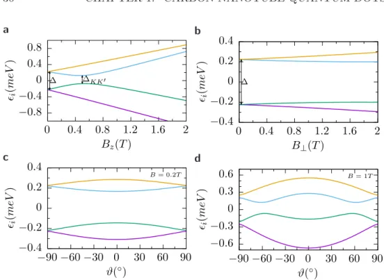
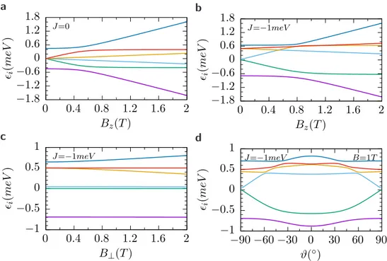
3.3 Virtual transitions in magnetospectroscopy . . . 73
3.3.1 Electron side: co-tunneling . . . 73
3.3.2 Hole side: Kondo peaks . . . 76
3.4 Role of Kramers pseudospin . . . 81
3.5 Angular dependence . . . 83
3.6 Conclusions and Outlook . . . 85
4 Dark states in a CNT-QD 87 4.1 Experimental signatures of CPT . . . 90
4.2 Model and dark states . . . 93
4.2.1 One-electron dark states . . . 96
4.2.2 Two-electrons dark states . . . 97
4.3 Dark state dynamics . . . 99
4.4 Precession, temperature and relaxation . . . 102
4.5 The tunneling rate matrix . . . 104
4.5.1 Tunneling amplitude . . . 104
TABLE OF CONTENTS vii
4.5.2 Single particle rate matrix . . . 106
4.5.3 Dark states . . . 108
4.6 Conclusions . . . 110
II Full counting statistics for multisite conductors 113 5 Full counting statistics 115 5.1 Counting variable . . . 116
5.2 Poissonian Noise and the Fano factor . . . 117
5.3 Generalized master equation . . . 118
5.3.1 Hierarchy of master equations . . . 119
5.3.2 Relation to the iterative scheme for static transport . . 121
5.3.3 Hierarchy of equations for the moments . . . 121
5.4 Matrix-continued fractions . . . 122
5.5 Minimal models . . . 124
5.5.1 Single resonant level . . . 124
5.5.2 Fast and slow channel model . . . 126
5.5.3 Single impurity Anderson model . . . 128
6 Topological blockade in a dimer chain 131 6.1 Topology in condensed matter physics . . . 132
6.2 The Su-Shrieffer-Heeger model . . . 134
6.2.1 Edge states . . . 135
6.2.2 Chiral symmetry . . . 137
6.3 Edge state blockade . . . 137
6.3.1 Analytical limits . . . 139
6.3.2 Arrays with an odd number of sites . . . 144
6.3.3 Blocking mechanism and localization . . . 145
6.4 The driven SSH model . . . 146
6.5 Transport in the high-frequency regime . . . 147
6.5.1 Current suppression and edge-state blockade . . . 149
6.5.2 Shot noise and phase diagram . . . 150
6.6 Robustness . . . 151
6.6.1 Static disorder . . . 153
6.6.2 Quantum dissipation . . . 154
6.7 Conclusions . . . 155
7 Dark states in a symmetric TQD 157
7.1 Model and spectrum . . . 159
7.2 Current and Fano maps . . . 165
7.3 Dark states of a symmetric TQD . . . 168
7.4 Interference blockade at the 2–3 resonance . . . 170
7.5 Interference blockade at the 5–6 resonance . . . 172
7.5.1 Hole transport . . . 172
7.5.2 Interference dynamics . . . 173
7.5.3 Including 4–particle ground states . . . 174
7.6 Robustness . . . 175
7.7 Conclusions . . . 176
Conclusions and outlook 179
A The rules of superoperators 183
B Additional checks of Kondo blockade 189
C Carbon nanotube eigenstates 195
D Rate matrix of a ring-metal complex 203
List of Figures 207
List of Tables 210
Acronyms 211
Bibliography 213
List of publications
Part of the work presented in this thesis has given rise to the following publications and preprints:
P.1 Edge-state blockade of transport in quantum dot arrays.
M. Benito, M. Niklas, G. Platero, and S. Kohler, Phys. Rev. B 93, 115432 (2016).
P.2 Transport, shot noise, and topology in AC-driven dimer arrays.
M. Niklas, M. Benito, S. Kohler and G. Platero, Nanotechnology 27, 454002 (2016).
P.3 Full-counting statistics of time-dependent conductors.
M. Benito, M. Niklas and S. Kohler, Phys. Rev. B 94, 195433 (2016).
P.4 Blocking transport resonances via Kondo many-body entanglement in quantum dots.
M. Niklas, S. Smirnov, D. Mantelli, M. Margańska, N. Nguyen, W. Werns- dorfer, J. Cleuziou and M. Grifoni, Nat. Commun. 7, 12442 (2016).
P.5 Fano stability diagram of a symmetric triple quantum dot.
M. Niklas, A. Trottmann, A. Donarini and M. Grifoni, Phys. Rev. B 95, 115133 (2017).
P.6 Dark states in a carbon nanotube quantum dot.
A. Donarini, M. Niklas, M. Schafberger, N. Paradiso, C. Strunk and M. Grifoni, arXiv:1804.02234 (2018).
ix
Abstract
I
nteractions play a major role in condensed matter due to their drastic influence on the many-body physics. This thesis is devoted to understanding their impact on transport problems through quantum mechanical systems using analytical and numerical tools. It comprises two main parts.First, we derive a quantum master equation to compute the reduced density matrix of the central system. It is based on a superoperator formalism that allows one to work in the weak coupling regime, as well as to define diagrammatic rules that can describe higher order transport. In this first part we deal with carbon nanotube (CNT) based quantum dots, whose high tuneability of the coupling strength with a back gate, allows us to study both, the weak and intermediate coupling regime.
In the latter we find an SU(2)⊗ SU(2) Kondo effect in CNTs due to the presence of spin and valley degrees of freedom. By inspecting magnetotransport measurements we discover that one transition, which however, is present in the weak coupling regime, is suppressed. Further analysis shows that using a pseudospin description of the degrees of freedom, only transitions that flip this pseudospin are allowed, which results in the said blocking. Our results show a robust formation of entangled many-body states with no net pseudospin.
In the weak coupling regime we find evidence for all-electric coherent population trapping in a CNT where the electrons become blocked in a dark state. Their emergence is visible in a distinct current-voltage characteristics with missing current steps and negative differential conductance, which requires a valley (angular momentum) and lead dependent tunneling phase. Coupling to the leads results in precession between the dark and coupled states, lifting the otherwise perfect blockade and creates a smooth current behavior.
The second part examines the statistical properties of open quantum systems. Using the full counting statistics formalism withing the master equation approach allows us to obtain the current variance, called shot noise,
xi
and higher order cumulants. We develop an efficient scheme to compute these cumulants for driven, multisite quantum dots. Interactions can affect the shot noise in two ways. Coulomb repulsion results in sequential tunneling events with little variance and a low shot noise. However, when interactions prevent electrons to leave the system, they can tunnel in bunches resulting in drastically increased shot noise.
We show that the Su-Schrieffer-Heeger model supports topological edge states that block the current. The shot noise can be used to distinguish this topological blockade from a standard blockading situation. The model requires variable hopping parameters in the chain of quantum dots to explore the topological phase transition, which might not be easily achievable in experiments. We propose an AC driving field to effectively tune these hopping parameters and use the shot noise to map out the topological phase diagram as function of the driving field parameters.
Since the shot noise can be used to unravel blocking mechanisms and their electron bunching, we apply the gained knowledge to the case of dark states.
This time we find dark states in a symmetric, triangular, triple quantum dot setup, based on local tunneling. In the angular momentum basis these dark states have the same, simple form as in the CNT case, allowing us to find analytic expressions for the current and the shot noise.
Introduction
O
ne of the most fundamental problems of physics in the beginning of the 20th century was the question whether light can be described in terms of particles or as waves. Both aspects have sooner or later been proven to be right. On the one hand, light must behave like waves since it exhibits the Doppler effect as well as interference. The latter was already shown in 1801 by Young [1] in his famous double-slit experiment, sketched in Fig. 1a. The resulting interference pattern on the screen can only be explained by the wave nature of light, cfg. Fig. 1b. On the other hand, ever since the explanation of the photoelectric effect by Einstein [2], it is clear that light must consist of elementary particles, the photons. About this seemingly contradiction Einstein and Infeld [3, p.278] wrote:But what is light really? Is it a wave or a shower of photons?
There seems no likelihood for forming a consistent description of the phenomena of light by a choice of only one of the two languages.
It seems as though we must use sometimes the one theory and sometimes the other, while at times we may use either. We are faced with a new kind of difficulty. We have two contradictory pictures of reality; separately neither of them fully explains the phenomena of light, but together they do.
Actually, this wave-particle duality can be extended to all particles as shown by de Broglie [5] and is nowadays a key concept of quantum mechanics.
Performing the double-slit experiment with electrons shows this duality. With a low electron density one observes single spots on the screen, revealing the localized particle nature of the electrons. This is displayed in Figs. 1c,d.
Steadily increasing the measuring time unveils their wave nature since the interference pattern appears, as seen in Figs. 1e,f. Such experiments have been repeated for molecules consisting of hundreds of atoms which still show
1
a
source double-slit screen b
c d
e f
Figure 1: Double slit experiment. aExperimental setup. b Original drawing by Young [1], showing interference of waves. c-f Experimental images from the screen using electrons, for increasing experiment time; from Bachet al. [4].
c,dThe completely random but point-like positions of the electrons highlight their particle nature. e,f With more electrons the interference pattern becomes apparent, underlying the wave nature of electrons.
the same results [6]. This allows one to describe the behavior of all mass-full particles by a wave equation [7]
𝑖ℏ𝜕
𝜕𝑡|𝜓(𝑡)⟩= ^𝐻|𝜓(𝑡)⟩, (1) the so called Schrödinger equation. This leads to the interesting observation that electrons can move through a barrier that they classically shouldn’t be able to move through. The solutions of the Schrödinger equation don’t end abruptly at a wall or barrier, they only taper off exponentially quick. Then, if the barrier is thin enough, the electron’s wave function is finite on the other side. The process of an electron moving through a barrier in this fashion is called quantum tunneling and is shown in Fig. 2a. The next logical step is to analyze what happens to electrons that pass more intricate junctions, like two consecutive
INTRODUCTION 3
a inc. b c
transm.
refl.
barrier constr.
destruct. 𝐸1
𝐸2
Figure 2: Transmission through junctions. aAn incident wave splits up into a transmitted and a reflected wave, when hitting a barrier. This results in quantum tunneling. Inside the barrier the wave function decays exponentially quick. b Fabry-Pérot interferometer. Depending on the phase difference of the wave passing both barriers and the wave getting reflected twice or more times, these waves interfere constructively or destructively. c If the barriers become wide, this situation resembles a quantum well with particle in a box-like states of discrete energy values.
barriers. If these barriers are thin enough, such that a large portion of electrons can tunnel through them, but also a comparative amount gets reflected, this resembles a two-path interference experiment. Such a generalization of the double-slit experiment, is called Fabry-Pérot interferometer, named after its developers [8, 9] and displayed in Fig. 2b. The beam of particles passing through both barriers interferes with the beams that get reflected twice or more times. Whether the two waves interfere constructively or destructively solely depends on their phase difference. The results so far are quite general and work for both, light and electrons.
At this point, the natural question arises whether the same effects are observable for electrons belonging to a solid-state system. In conductors, barriers can be created simply by building heterostructures using layered materials or depletion gates. In principle, this allows to perform Fabry- Pérot experiments in patterned materials. However, electrons can behave fundamentally different than photons since they are fermions and are subject to interaction. In particular, scattering processes, e.g. mediated by phonons, can destroy the phase coherence due to their stochastic nature. Therefore, in order to see any quantum phenomena of electrons, the system’s size must be small compared to the phase coherence length. At low temperatures, this allows the construction of devices at scales comparable with the electron’s de Broglie wavelength and, accordingly, the observation of quantum interference effects in the solid state. For example, Fabry-Pérot interference with electrons
has been measured in carbon nanotube waveguides [10, 11]. In the limit of thin barriers, or said in other words, in the limit of large tunnel coupling, electron-electron interaction effects have almost no importance. In this regime, Green’s functions based methods allow for the description of non-interacting electron transport. As the tunnel coupling becomes weaker, i.e. the barriers become thicker, the situation resembles more and more a quantum well, as seen in Fig. 2c. The electrons get confined in the region between the two barriers and form particle in a box-like states with discretized energy levels. The tunneling through the leads only acts as a weak perturbation in this case. In reality, we deal with three dimensional materials. A patterned device that spatially restricts electrons in all three dimensions, which results in bound states, is called quantum dot. Consequently, the precise geometry and level alignment of the inter-barrier region will increasingly affect the transport properties.
The resulting localization of the electrons lets electron-electron interactions become more and more important. For very small sizes this interaction can even become the largest energy scale of the whole setup and separate states of different electron numbers on the quantum dot [12, 13]. In this thesis we deal with transport properties through such interacting nanojunctions. The control of the precise electron number in the quantum dot forms the basis for many realizations of spin or charge qubits [14]. While quantum information processing requires quantum coherence and therefore optimal isolation from the environment, the possibility to couple quantum dots to this environment through the barriers may be useful as well. It not only can be exploited for qubit readout [15], but also allows one to determine the relevant system parameters. Multiple qubits or more sophisticated qubits can be created by using a quantum dot with additional degrees of freedom, like the two valleys in graphene or carbon nanotubes, or simply multiple quantum dots in close proximity.
The particle wave duality will not only lead to quantum interference effects and many-body entanglement but will also influence the statistical properties of electron transport. This can be used to obtain information about the underlying transport processes by measuring e.g. the variance of the current, called shot noise. Compared to the average current, the shot noise reveals whether electrons tunnel avalanche-like or in an equidistant manner.
Summarizing in the words of Landauer [16]: “The noise is the signal”.
INTRODUCTION 5
Outline
This thesis splits into two parts, dealing with transport across carbon nanotube (CNT) quantum dots and the noise properties of multiple quantum dot systems,
respectively.
Part I The first part starts with an introduction into the physics of transport in quantum dots and we derive a quantum master equation that allows its theoretical description. Using the special electric properties of CNTs, we apply the theory in the intermediate coupling regime, where we find that certain resonances of the Kondo effect become blocked. In the weak coupling regime we encounter dark states as superpositions of degenerate valley states that block the current in a unique way.
Chapter 1. Carbon nanotube quantum dots
In this chapter we introduce the concept of single electron transistors.
Following a simple capacitor model, one can distinguish between a Coulomb blockade regime and a transport regime. Only at Coulomb blockade a fixed number of electrons is trapped on the quantum dot, which prevents current flow. Furthermore, we obtain the electrical properties of CNT quantum dots.
Starting from the dispersion of graphene and applying boundary conditions, allows us to write a model Hamiltonian using spin and valley quantum numbers.
Chapter 2. Transport theory
To calculate the current through single electron transistors we derive a quantum master equation for the reduced density matrix of the central quantum dot. We use a superoperator approach based on the Nakajima- Zwanzig projector operator formalism. This allows us to describe transport to all orders in a diagrammatic way. We show that in the weak coupling regime it gives the same result as traditional derivations. Additionally, it makes the resummation of certain diagrams possible, which enables us to, at least to some extent, describe strong coupling.
Chapter 3. Blocking Kondo resonances in quantum dots
In CNT quantum dots the coupling strength is tunable via the gate voltage.
On the hole side the Kondo effect is dominant in transport. After an introduc- tion to the spin-1/2 Kondo effect, we extend it to the SU(2) ⊗SU(2) Kondo effect in CNTs. This requires an analysis of the symmetries present in the single particle spectrum of a CNT. We find time-reversal like, particle-hole like and chiral symmetries. Magnetospectroscopy experiments reveal that in the
Kondo regime the transitions to states related by particle-hole like symmetry are blocked, despite existing on the electron side in co-tunneling resonances.
Chapter 4. Dark states in a carbon nanotube quantum dot
In CNTs with vanishing spin-orbit coupling and valley mixing, the valley (orbital) degeneracy supports the formation of dark states. We find analytic expressions for these dark states build upon an orbital dependent tunneling phase. Solving a minimal model for only𝑁 = 0↔1 transitions, we find an analytic expression for the current. The resulting𝐼−𝑉 characteristics is unique and quantitatively fits the experiment. We give a microscopic justification of the tunneling phase, based on the surface Γ–point approximation.
Part II This part opens with an introduction to the statistical properties of transport and a theoretical framework to calculate it within the master equation approach. We apply this method to identify topological blockading situations in a dimerized chain of quantum dots. We use the noise map to unravel the influence of orbital dark states in a ring of three quantum dots.
Chapter 5. The framework of full counting statistics
In this chapter we describe full counting statistics, a way to compute all current cumulants within the master equation approach of chapter 2. The resulting generalized master equation can be solved iteratively to first compute the current, then the noise, followed by all higher order cumulants. We find a numerically effective way to compute this cumulants for driven systems.
Chapter 6. Topological blockade in a dimer chain
We introduce the key concepts of topology and the Su-Schrieffer-Heeger model. This model can be build as a dimerized chain of quantum dots which supports edge states that can block the current. We analyze certain limits of this topological blockade and find the Fano factor as an efficient indicator to measure the topological phase. An AC driving field renormalizes the hopping amplitudes and, in turn, allows one to control topological phase transitions.
Chapter 7. Dark states in a symmetric triple quantum dot
In the last chapter we analyze the simplest model that supports dark states through orbital degeneracies and at the same time allows one to treat interactions exactly: a C3𝑣 symmetric triangular triple quantum dot. We find all its eigenstates in analytic form, which allows us to obtain simple expressions for the dark states, in complete analogy to chapter 4. We find certain fractional values of the Fano factor that can be explained via minimal models.
Part I
Transport across interacting carbon nanotube quantum
dots
7
C h a p t e r
1
Carbon nanotube quantum dots
T
he possibility of spatially restricting charge carriers on length scales comparable to their wavelength is at the very heart of mesoscopic condensed matter physics. One of the simplest realizations that takes advantage of the quantum nature of electrons are artificial atoms or quantum dots (QDs), isolated islands which are confined in all three spatial directions.Their electronic properties approximately follow from a simple particle in a box model in which the energies of the bound states depend on the size of the QD.
This effect is already extensively used in optics to produce fluorescent light of a single wavelength in a controllable way. Slowly this technology even finds its way into everydays electronics like TVs. Due to the small size, interactions play a dominant role in QDs, most importantly Coulomb interaction. Adding an additional electron to a charged QD requires enough energy to overcome its Coulomb repulsion with the electrons on the dot. These striking electronic properties are also interesting for electronic applications and especially for integrated circuits. Besides from being promising candidates for Qubits used in quantum computers, they allow for a nano scale analogue to a transistor, a so called single electron transistor.
A promising candidate for such QDs are carbon nanotubes (CNTs), in the last decades they were actively studied not only in physics. Their extraordinary mechanical properties, first of all their large stiffness [17], makes them ideal candidates to build lightweight and strong materials. In medicine CNTs
9
are considered a likely contestant for drug delivery mechanisms [18]. With transparencies ranging from 85% [19] to only 0.01% [20] thin films of CNTs can operate as transparent electronics and prevent stray light in telescopes.
We will analyze the structure of bound states in a single CNT-QD and its influence on transport.
1.1 The single-electron transistor
A transistor is a three terminal device where the current through two of these terminals, called source and drain, can be mediated via the third contact, called gate. In classical semiconductor transistors like the metal-oxide-semiconductor field-effect transistor (MOSFET) an applied gate voltage changes the charge carrier density between the source and drain and can create depletion regions which block the current flow. Scaling down MOSFETs presents the semicon- ductor industry with large problems since the electron number becomes small enough for quantum effects, like losses via tunneling through insulators, to play more and more important roles.
A possible solution to these problems is the implementation of a new generation of transistors that actively takes advantage of the electrons quantum nature. One of them is the so called single-electron transistor (SET) where the gate contact is capacitively coupled to a central QD and allows the control of the precise electron number on the dot up to single electrons via the gate voltage𝑉g. The source and drain contacts in SETs are typically coupled to the QD via tunneling barriers. A voltage applied between these two terminals is called bias voltage𝑉b. In Fig. 1.1 a scheme of such a SET is shown where the left (L) and right (R) leads can play the roles of source and drain depending on the bias direction. The gate voltage is often applied via a back gate contact.
The behavior of a SET depends strongly on various parameters such that one can identify different transport regimes.
1.1.1 Transport regimes
The transport properties of a SET are mainly influenced by three parameters.
First, the charging energy of the QD,𝑈, which originates from the Coulomb repulsion of electrons. Second, the temperature of the environment, 𝑇, and third, the coupling strength between the contacts and the QD, usually expressed in tunneling rates Γ. In the limit of strong coupling where𝑈, 𝑘B𝑇 ≪ℏΓ, the two
1.1. THE SINGLE-ELECTRON TRANSISTOR 11 𝑉b
𝑉g
Figure 1.1: Scheme of a single electron transistor. Two large reservoirs, L and R, are tunnel coupled to a central QD. The gate voltage 𝑉g influences the charge on the QD.
interfaces act as semi-transparent mirrors leading to Fabry-Pérot interference.
This limit is not part of this thesis but studied e.g. in CNT-QDs in Dirnaichner et al.[11]. Decreasing the coupling strength until𝑘B𝑇 ≪ℏΓ≪𝑈, the contact electrons are mostly scattered by an electron in the QD which is known as the Kondo effect. We analyze and further introduce this regime in Sec. 3 at the example of a CNT-QDs. In the weak coupling regime where ℏΓ≪𝑘B𝑇 ≪𝑈, the coupling is so much suppressed that only a single electron tunnels at a time. This so called sequential tunneling can only be extended for slightly stronger coupling strength when higher order processes like co-tunneling play a role. Most parts of this thesis are performed in this limit.
1.1.2 Capacitor model of metallic islands
A first step in understanding the influence of the three terminals on transport properties is the analysis of the classical circuit corresponding to a SET setup.
There, the three leads are capacitively coupled to the QD with capacitances 𝐶L, 𝐶R and 𝐶g. In addition, the left and right contact allow for tunneling to the central QD. They are considered as large reservoirs of electrons such that they stay invariant upon adding or removing electrons. Their states are filled up to the Fermi level or electro-chemical potential which are controlled by applying the bias voltage. For simplicity we refer to the electro-chemical potential only as chemical potential in the following. The bias is applied to a certain amount 0 ≤ 𝜂 ≤ 1 on the left lead and the rest to the right lead.
This results in the chemical potentials𝜇L=𝜇0+𝜂𝑉b and𝜇R =𝜇0+ (𝜂−1)𝑉b
for the left and right lead, respectively, where for convenience we set 𝜇0 = 0.
We first consider a simple metallic QD where the electrons do not have any internal degrees of freedom, like spin, and can be added without restrictions.
In this quasi classical picture the only quantum effect is the quantized charge on the dot which can be precisely controlled. The induced charge on the QD is then𝑄𝑖=𝐶g𝑉g+𝐶L𝜂𝑉b+𝐶R(𝜂−1)𝑉b. Accounting for a charged QD with𝑁 electrons, the total charge is𝑄=𝑄𝑖+𝑒𝑁, where 𝑒is the negative elementary charge. The energy of the QD is the one of a classical capacitor
𝐸𝑁 = 𝑄2
2𝐶 = (𝑒𝑁+𝐶g𝑉g+𝐶L𝜂𝑉b+𝐶R(𝜂−1)𝑉b)2
2𝐶 , (1.1)
with the total capacity of the QD, 𝐶=𝐶L+𝐶R+𝐶g. The energy required to add an additional electron or to remove one, usually defined as chemical potential, is then given by the energy difference of two consecutive states
𝜇𝑁 =𝐸𝑁 −𝐸𝑁−1= 𝑒2 𝐶
(︂
𝑁−1 2
)︂+𝛼g𝑉g+𝛼L𝜂𝑉b+𝛼R(𝜂−1)𝑉b, (1.2) with the conversion factors 𝛼𝑥=𝑒𝐶𝑥/𝐶.
1.1.3 Coulomb blockade
For simplicity we initially allow only a minimal bias voltage |𝑒𝑉b|≲𝑘B𝑇 to obtain a finite current𝐼 or differential conductance 𝐺= d𝐼/d𝑉b, for vanishing bias, called linear conductance. The condition to add electrons to the QD is that an electron with larger energy than the chemical potential of the dot is available in the leads, this means𝜇𝑙≳𝜇𝑁, for 𝑙= L or R. At the same time we require this electron to be able to leave to the other lead which requires free states there and therefore𝜇¯𝑙 ≲𝜇𝑁. The only way these two conditions can be fulfilled at the same time at almost vanishing bias is that the chemical potential of the QD is in resonance with the chemical potentials of both leads
𝜇L≈𝜇𝑁 ≈𝜇R. (1.3)
This situation is shown in a chemical potential landscape along the SET in Fig. 1.2a. If the chemical potential of the dot is below the lead chemical potentials the QD is filled with 𝑁 electrons which cannot escape and no current can flow. This situation is called Coulomb blockade and is named after the Coulomb force, ultimately responsible for this effect. A Coulomb blocked SET is shown in Fig. 1.2b. Experimental analysis of this effect is quite easy upon realizing that the chemical potential of the QD in Eq. (1.2) depends
1.1. THE SINGLE-ELECTRON TRANSISTOR 13 a
𝜇𝑁−1 𝜇𝑁
𝜇𝑁+1
𝜇L 𝜇R
𝑉g
b
𝜇𝑁−1 𝜇𝑁 𝜇𝑁+1
𝑉g
Figure 1.2: Chemical potential landscape of the SET at zero bias. aIn the resonant case the chemical potential of 𝑁 electrons 𝜇𝑁 is aligned with the Fermi energy of the two leads. b The gate voltage allows to shift the chemical potentials down such that the 𝑁-th electron can enter but not leave anymore.
The QD is in Coulomb blockade.
linearly on the gate voltage. Therefore, 𝑉g can be used to shift the chemical potential and the linear conductance as a function of 𝑉g should show peaks exactly around the resonance conditions. The distance between two of these peaks is constant and is naturally the difference of two consecutive chemical potentials corrected by the gate conversion factor
𝛼gΔ𝑉g =𝜇𝑁 −𝜇𝑁−1 = 𝑒2
𝐶 ≡𝑈, (1.4)
also known as charging energy 𝑈. These repeated peaks are called Coulomb oscillations. One of the first experimental realizations from 1991 can be seen in Fig. 1.3. Between two peaks the number of electrons on the QD stays constant and increases by one with each peak. Therefore, these regions are also called stable regions. The next step in understanding the transport properties of SETs is to allow for larger bias voltages.
1.1.4 Non-linear transport
The results of Coulomb oscillations can easily be extended to the non-linear transport regime with a finite bias voltage. The plot of the current or differential conductance vs both gate and bias voltage is called (charge) stability diagram.
It is best understood by looking at the chemical potential landscape again.
The conditions for adding and removing electrons stay unchanged, only now
Figure 1.3: Experimental linear conductance as a function of𝑉gshows Coulomb oscillations in a GaAs-QD at various temperatures. Taken from Meir et al.
[21].
allow for a larger range of current flow. The combined conditions now read 𝜇L≥𝜇𝑁 ≥𝜇R for 𝑒𝑉b >0,
𝜇L≤𝜇𝑁 ≤𝜇R for 𝑒𝑉b <0. (1.5) As long as no chemical potential of the QD is in the bias window spanned by the two chemical potentials of the leads, the system is in Coulomb blockade.
This is illustrated in Fig. 1.4a. As soon as a chemical potential enters this windows there is a peak in the differential conductance and current can flow as shown in Fig. 1.4b for positive chemical potential drop. This leads to a diamond shaped pattern of zero current in the stability diagram as shown in Fig. 1.5a. The current outside of these so called Coulomb diamonds reaches a plateau of constant current which depends on the tunneling rates and only changes once an additional chemical potential enters the bias window. The asymmetric application of the bias voltage on the two contacts with the factor 𝜂= 0.4 causes tilted Coulomb diamonds.
So far the quantum nature of the central QD has been neglected by assuming a metallic character. The inclusion of such quantum mechanical effects apart from quantized charges can have many interesting consequences.
The trivial change of the energies for different particle numbers results in Coulomb diamonds of different heights. Degeneracies can influence the current height and special shapes of wave functions can even lead to annihilation of
1.1. THE SINGLE-ELECTRON TRANSISTOR 15 a
𝜇𝑁−1 𝜇𝑁 𝜇𝑁+1
𝑉g
𝑒𝑉b
b
𝜇𝑁−1 𝜇𝑁
𝜇𝑁+1
𝑉g
𝑒𝑉b
Figure 1.4: Chemical potential landscape of the SET at finite bias. aThe chemical potential of the dot is lower than both chemical potentials of the contacts leading to Coulomb blockade. b Current can flow since a chemical potential of the QD is in the bias window.
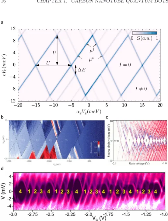
tunneling matrix elements with resulting current suppression. The details then strongly depend on the underlying model. In Figs. 1.5b-d various experimental stability diagrams for different types of QDs are shown. All of them feature differently sized Coulomb diamonds. In the experimental stability diagrams additional lines outside the Coulomb diamonds can be seen. These derive from excited states that can change the current once their chemical potential enters the bias window.
1.1.5 Excited states
The next step in analyzing quantum effects in a SET is to look at the influence of excited states. In the simple case that there exists a single excited state with 𝑁 electrons at an energy 𝐸𝑁* > 𝐸𝑁, one can define two new chemical potentials
𝜇*𝑁 =𝐸𝑁* −𝐸𝑁−1,
𝜇†𝑁+1=𝐸𝑁+1−𝐸𝑁*, (1.6) which both give rise to additional lines outside the Coulomb diamonds. Inside the Coulomb diamonds the current is still zero since 𝑁 electrons are already trapped on the QD in the ground state and therefore the excited 𝑁-particle state is not available for transport. In Fig. 1.5a the positions of the additional lines due to an excited state with 𝐸𝑁* −𝐸𝑁 = Δ𝐸 are marked. In the experimental stability diagrams in Figs. 1.5b-d many such excited state lines are visible suggesting complex level structures.
a
−12
−8
−4 0 4 8 12
−20 −15 −10 −5 0 5 10 15 20 eVb(meV)
αgVg(meV)
−12
−8
−4 0 4 8 12
−20 −15 −10 −5 0 5 10 15 20
0 G(a.u.) 1
U
U µ†
µ∗
∆E I = 0
I 6= 0
b c
d
Figure 1.5: aStability diagram of a QD with 𝑈 = 10𝑚𝑒𝑉, 𝑘B𝑇 = 0.1𝑚𝑒𝑉 and𝜂= 0.6. The width and height of the Coulomb diamonds are given by the charging energy 𝑈. The central Coulomb diamond features a single excited state with Δ𝐸 = 3𝑚𝑒𝑉. Its excitation lines are marked by arrows. b,c,d Experimental stability diagrams where the central QD is an InSb nanowire in the hole regime (b), a GaAs heterostructure (c), or a single-walled CNT (d). Figures taken from Pribiag et al. [22], Kouwenhoven and Oosterkamp
[23], Sapmazet al. [24].
1.1. THE SINGLE-ELECTRON TRANSISTOR 17
a
b
c
d
𝜇𝑁−1 𝜇𝑁 𝜇𝑁+1
𝜇𝑁−1 𝜇𝑁 𝜇𝑁+1 𝜇𝑁−1
𝜇𝑁 𝜇𝑁+1
𝜇𝑁−1 𝜇𝑁 𝜇𝑁+1 electron-like
hole-like
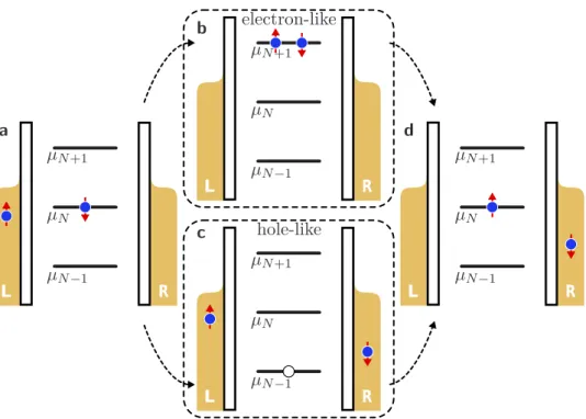
Figure 1.6: Co-tunneling process in a chemical potential landscape. aStarting point is 𝑁 electrons in the QD. b,c Virtual transition state for electron-like (b) and hole-like (c) processes that temporarily violate energy conservation. d After the second electron tunnels the total energy of the co-tunneling process is conserved.
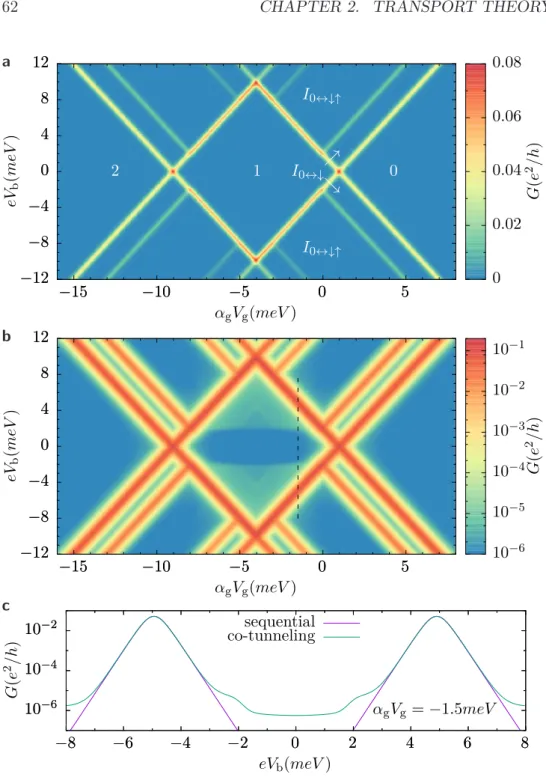
If the tunneling rates are not too small, higher order effects can play a role that extend the picture of sequentially tunneling electrons.
1.1.6 Co-tunneling
The next leading order correction of contributions from tunneling between the leads and the QD includes all mechanisms of fourth order in the tunneling Hamiltonian𝒪( ^𝐻tun4 ) (or analogously second order in the tunneling rate𝒪(Γ2)) and therefore contains all processes where two electrons tunnel at the same time.
This gives rise to so calledpair tunnelingwhich describes two electrons tunneling simultaneously from a lead onto the QD or reverse. These processes occur when the chemical potential of a lead matches the average of two subsequent charging energies, so exactly in the middle of two sequential tunneling lines [25]. The second possibility of second order processes is co-tunneling where again two electrons tunnel simultaneously but one starts in a lead while the
a b
Figure 1.7: Scanning electron microscopy images of ultra-clean, suspended CNT-QD devices. Figures originate fromaGrenoble [P.4] andb from Regens- burg [26].
other one starts in the QD. Such tunneling events can be interpreted as two entangled tunneling events connected by a virtual state. Depending on which electron tunnels first, this virtual state can be either electron-like or hole-like.
If the final state of the QD electron has the same energy as the initial one, such a process is calledelastic co-tunneling, which is displayed in Fig. 1.6. The intermediate states are called virtual since they would violate the conservation of energy even though the total process conserves the energy. Since such processes are always possible, independent of the bias and gate voltage, this leads to a finite differential conductance inside the Coulomb diamonds. If excited state exist in the system it is possible to see inelastic co-tunneling which occurs if the final and initial state have different energies. This creates an additional step in the differential conductance inside the Coulomb diamond at the bias voltage that matches the level splitting of the excited state, i.e.
exactly at the position where the excited state sequential tunneling line enters the Coulomb diamond.
1.2 Electronic properties of carbon nanotube quantum dots
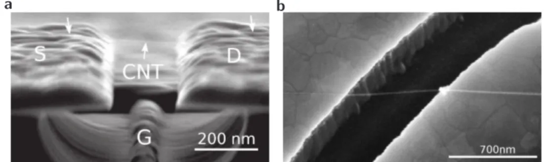
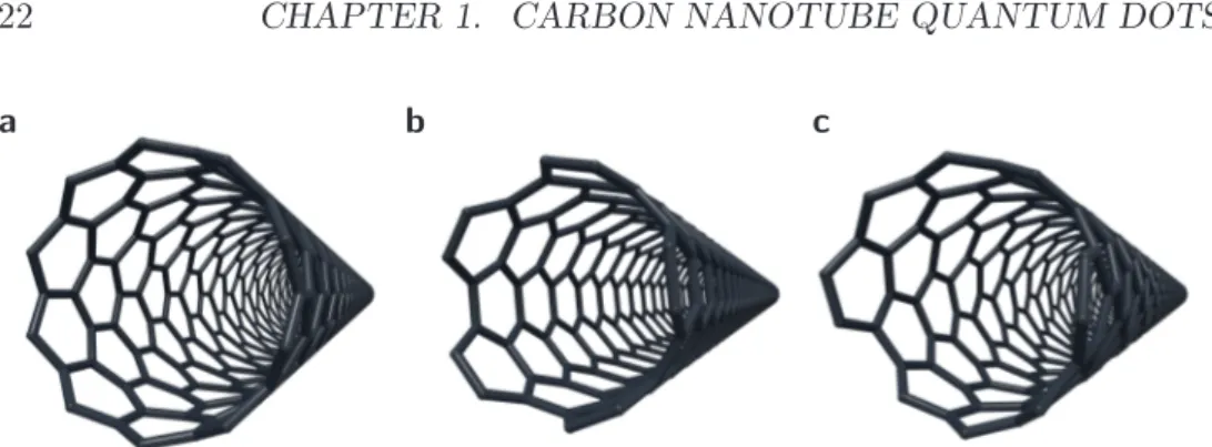
Fullerenes are molecules of carbon, typically in a hollow form and often with high symmetry. Next to spheric molecules like C60, often called buckyballs, cylindrical fullerenes are called carbon nanotubes (CNTs). They are ideal candidates for QDs since the charge carriers in CNTs are already confined in two dimensions such that contacting a tube on both ends automatically creates a QD. In Fig. 1.7 two such devices are shown where the CNT was
1.2. ELECTRONIC PROPERTIES OF CNT-QDS 19
a b
𝑥 𝑦
𝑎1
𝑎2 𝐴
𝐵
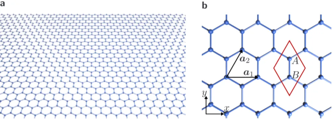
Figure 1.8: aA single layer of graphene is a honeycomb lattice of carbon atoms.
b The unit cell of graphene consists of two sublattices,𝐴and𝐵 and is marked in red. The lattice is created by repeating this unit cell with the lattice vector 𝑎1 and 𝑎2.
grown as last fabrication step over the predefined, litographically fabricated contacts which creates ultra-clean, suspended CNT-QDs. The atomic structure of CNTs is similar to graphene, a two-dimensional sheet of linked hexagonal rings. Therefore, it is quite natural to consider CNTs as rolled up graphene to derive their electronic properties.
1.2.1 Graphene
The honeycomb lattice of graphene is shown in Fig. 1.8a. It is spanned by duplicating the unit cell over and over shifted by multiples of the translational vectors𝑎1/2. This unit cell consists of a two atom sublattice𝑝=𝐴, 𝐵. This is illustrated in Fig. 1.8b. Fourier transforming the graphene lattice into reciprocal space results in a hexagonal first Brillouin zone whose edges are called Fermi points. There are only two geometrical independent Fermi points labeled𝐾 and𝐾′, as shown in Fig. 1.9a. The tight binding Hamiltonian with nearest neighbor hopping between the 𝑝𝑧 orbitals is written in sublattice basis, where it reads
ℋ0=
(︃ 0 𝛾(𝑘) 𝛾*(𝑘) 0
)︃
, (1.7)
with𝛾(𝑘) =⟨𝐴|ℋ0|𝐵⟩=𝑡(1+𝑒𝑖𝑘𝑎1+𝑒𝑖𝑘𝑎2) =𝑡(1+𝑒𝑖√3𝑘𝑥𝑎C+𝑒𝑖(√3𝑘𝑥+3𝑘𝑦)𝑎C/2).
Here, 𝑎C is the atomic bond length and 𝑡 the hopping integral. The emerging dispersion relation with a valence and a conduction band 𝐸(𝑘) =±|𝛾(𝑘)|is shown in Fig. 1.9b. Starting from this two dimensional band structure one can obtain the one dimensional bands of CNTs by rolling up a stripe of graphene.
a
𝐾′
𝐾 𝑘𝑥
𝑘𝑦
−2 −kx1 0 1 2(a−C1) −20 2 ky(a−1C )
−3
−2
−1 0 1 2 3
E(t) b
Figure 1.9: aFirst Brillouin zone of graphene in reciprocal space. The two Fermi points are𝐾and𝐾′. bDispersion relation of graphene with the Brillouin zone highlighted. The conduction and valence band touch at the Fermi points.
1.2.2 Classification of carbon nanotubes
Starting from a large patch of graphene it is possible to construct a CNT by picking up any two non-neighboring unit cells and bringing them together by rolling up the sheet. The vector connecting these two unit cells 𝐶 = 𝑚𝑎1 +𝑛𝑎2 ≡ (𝑚, 𝑛) is called chiral vector and can be written as a linear combination of the lattice vectors. The corresponding prefactors are the chiral indices and completely define the structure or chirality of the tube. Often the chirality is given by the radius of the tube 𝑅=𝑎C√︀3(𝑚2+𝑚𝑛+𝑛2)/2𝜋 and its chiral angle 𝜃= arcsin(√
3𝑛/(2√
𝑚2+𝑚𝑛+𝑛2)), the angle between the chiral vector and the𝑥-axis. The coordinate system of the CNT is the one of graphene rotated by the chiral angle. These coordinates are around the circumference𝑥⊥ and along the tube 𝑧. The new unit cell of the CNT is spanned by the chiral vector and the primitive translation 𝑇 in𝑧 direction.
This is illustrated for an (8,2) tube in Fig. 1.10. In this way one can recognize two special types of CNTs. Their names originate from the shape of edge of the tube. Inzig-zag CNTs the second chiral index is zero (𝑚,0) and therefore also the chiral angle is zero,𝜃= 0. The opposite limiting case is called armchair CNTs where both chiral indices are the same (𝑚, 𝑚). The chiral angle in these specimen is𝜃= 30∘. Both edge shapes are illustrated in Fig. 1.10. All intermediate tubes with 0< 𝜃 <30∘ are simply calledchiral CNTs. As we will see in a moment, the chiral CNTs can be classified into two categories: the
1.2. ELECTRONIC PROPERTIES OF CNT-QDS 21
𝑎1 𝑎2
𝑥 𝑦
𝑥⊥ 𝑧
𝜃
𝐶 𝑇
(8,2)
armchair
zig-zag
Figure 1.10: The chirality of the CNT is defined via the chiral indices at an example of a 𝐶 = (8,2) tube. The chiral angle 𝜃 rotates the coordinate system into the transversal 𝑥⊥ and longitudinal𝑧 one. The blue area is the translational unit cell of the resulting CNT which is defined by the chiral vector 𝐶 and the primitive translation 𝑇. The edges of the two special chiralities, the zig-zag and armchair one, are highlighted in red.
ziz-zag class and the armchair class tubes. Examples of these three classes can be seen in Fig. 1.11. The rolling up of the graphene sheet also affects its band structure since also the coordinate system in the reciprocal space is rotated by the chiral angle into 𝑘⊥ and𝑘𝑧. The new Brillouin zone of CNTs is rectangular and spanned by the reciprocal vectors corresponding to the new unit cell spanned by𝐶 and 𝑇. It has a width in 𝑘𝑧 direction of 2𝜋/|𝑇|. 1.2.3 Transverse quantization
The wave function has to be single-valued and continuous around the CNTs circumference which implies a quantization condition on the transverse mo- mentum
𝑘⊥(𝑥⊥+2𝜋𝑅) =𝑘⊥𝑥⊥+2𝜋𝑛𝑧, ⇒ 𝑘⊥= ℓ𝑧
ℏ𝑅, with 𝑛𝑧 = ℓ𝑧
ℏ ∈N. (1.8) Here,ℓ𝑧 is called angular momentum. This cuts the rectangular CNT Brillouin zone with lines parallel to 𝑘𝑧 as is indicated in Fig. 1.12a-c by red lines for
a b c
Figure 1.11: Examples of the three chirality classes. aA (10,0) zig-zag CNT with a chiral angle of 𝜃= 0. b A (5,5) armchair CNT with a chiral angle of 𝜃= 30∘. cA (8,2) chiral CNT with a chiral angle of 𝜃≈10.9∘.
three different CNTs. This process is called zone-folding since the bands are effectively folded from the graphene Brillouin zone into the CNT Brillouin zone.
Out of these cuts one obtains one dimensional bands shown for the three cases in Fig. 1.12d-f. Here, only the conduction band is shown since the valence band just differs by a minus sign. These bands feature two Fermi points where in the case of zig-zag CNTs they fall on top of each other at𝑘𝑧 = 0. Also it is clear that this divides CNTs into two categories, semiconducting like the (10,0) one and metallic like the (5,5) and (8,2) ones, depending on whether a band gap is opened or not. The condition to obtain a metallic tube is a quantization line hitting a Fermi point of graphene. This condition can be written for a general (𝑚, 𝑛)-CNT as
𝑚−𝑛 mod 3
⎧
⎨
⎩
= 0 metallic
̸= 0 semiconducting , (1.9) which means that one in three tubes and also all armchair CNTs are metallic.
In this thesis we will restrict ourself to metallic tubes only. We are interested in the low energy physics of the order of𝒪(𝑚𝑒𝑉). Applying a commonly used value for the hopping parameter 𝑡≈2.66𝑒𝑉 [27], one realizes that the bands lie in energy ranges of𝒪(𝑒𝑉) which is orders of magnitude larger than what we are interested in. This means that for the low energy physics only the lowest bands are important. The angular momentum of these bands allows to classify all CNTs into two groups, thearmchair class tubes withℓ𝑧 = 0 and the zig-zag class tubes withℓ𝑧̸= 0. This property can be also be extracted from the chiral indices because every CNT is symmetric under rotations of 2𝜋/˜𝑛, where ˜𝑛= gcd(𝑚, 𝑛). This C˜𝑛symmetry allows to group all tubes according
1.2. ELECTRONIC PROPERTIES OF CNT-QDS 23
a (10,0)
−4
−2 0 2 4
−4 −2 0 2 4 ky(a−1 C)
kx(a−1C )
−4
−2 0 2 4
−4 −2 0 2 4
b (5,5)
−4 −2 0 2 4 kx(a−1C )
−4 −2 0 2 4
c (8,2)
−4 −2 0 2 4 kx(a−1C )
−4 −2 0 2 4 0 1 2 3
E(t)
d
0 1 2 3
−1 0 1
E(t)
kz(a−C1) 0
1 2 3
−1 0 1
e
−1 0 1 kz(a−C1)
−1 0 1
f
−0.5 0 0.5 kz(a−C1)
−0.5 0 0.5
Figure 1.12: a-cConduction band around the first Brillouin zone. Rolling up the graphene sheet creates quantized transverse momentum inside the CNT Brillouin zone. The resulting cuts are shown in red for a (10,0) (a), a (5,5) (b) and an (8,2) (c) CNT. The distance between two quantization lines is 1/𝑅.
d-f Corresponding conduction bands for the same chiralities.
to [28]
𝑚−𝑛 mod 3˜𝑛
⎧
⎨
⎩
= 0 armchair class
̸= 0 zig-zag class . (1.10) This shows that the (8,2) CNT from Fig. 1.12c is of the armchair class. De facto, all armchair class CNTs feature two Fermi points at opposite 𝑘𝑧 in the zone folded momentum space, while in the case of zig-zag class tubes both Fermi points cones fall on top of each other at 𝑘𝑧 = 0, like e.g. in Fig. 1.12d for a pure zig-zag tube.
1.2.4 Low energy expansion
As can be seen in Fig. 1.9b and in the lower panels of Fig. 1.12, at low energies 𝒪(𝑚𝑒𝑉) the dispersion is linear around the two Fermi points𝐾 and 𝐾′. Such band structures are usually referred to as Dirac cones since these effectively
massless electrons resemble the solutions of the relativistic Dirac equation.
This introduces a new quantum number in the system called valley 𝜏. In zig-zag class CNTs the valley is closely related to the angular momentum of the corresponding band. In armchair class tubes this assignment is not possible because both Dirac cones stem from a single band with only one angular momentum state. Therefore, the valley is not a good quantum number in armchair class CNTs. Using the fact that𝐾 =−𝐾′, the valley is defined via 𝑘 = 𝜏𝐾 +𝜅 where 𝜏 = 1 corresponds to the 𝐾 point and 𝜏 = −1 to the𝐾′ point. We know that in metallic tubes the quantization lines hit the Fermi point exactly and therefore𝜅⊥= 0 when neglecting all curvature effects.
Rotating the graphene Hamiltonian from Eq. (1.7) to the CNT coordinates and expanding it around the Fermi points results in
ℋ𝜏(𝜅𝑧) =
(︃ 0 𝛾𝜏(𝜅𝑧) 𝛾𝜏*(𝜅𝑧) 0
)︃
, (1.11)
where we use an extended space by defining ^𝜏3 as the third Pauli matrix in valley space. Here,
𝛾𝜏(𝜅𝑧) = ˜𝑡(^𝜏3𝜅𝑥−𝑖𝜅𝑦) = ˜𝑡(^𝜏3𝜅⊥−𝑖𝜅𝑧)𝑒𝑖𝜏^3(𝜃+𝜋3), (1.12) with ˜𝑡= 3𝑡/2. The resulting bands feature the Dirac cones centered around the Fermi points with 𝐸𝜏(𝜅𝑧) = ˜𝑡|𝜅𝑧|, where the valley does not influence the energy, only the phase in the Hamiltonian. This simple picture of rolled graphene is often not enough since curvature can play a major role, especially for CNTs with a small radius.
1.2.5 Effects of curvature, magnetic fields and boundaries The band structure of graphene is derived using only 𝑝𝑧 orbitals and the resulting Π bonds. The other orbitals in the 𝜎 bonds do not play any role because they are hybridized into the 𝑠𝑝2 orbitals that build the lattice and especially they are in-plane and therefore perpendicular to the𝑝𝑧 orbitals. In CNTs this picture changes and hopping through𝜎 bonds is possible due to the bending of the lattice and the resulting angles between the different orbitals.
These curvature effects create a valley dependent shift of the momentum Δ𝑘𝑐 in 𝑘⊥ and 𝑘𝑧 direction. It is important to notice that Δ𝑘𝑐⊥ ∝ cos(3𝜃) and Δ𝑘𝑐𝑧 ∝sin(3𝜃). Therefore, these shifts are in perpendicular direction for zig- zag CNTs and in 𝑘𝑧 direction for armchair CNTs. The exact form and the
1.2. ELECTRONIC PROPERTIES OF CNT-QDS 25 calculation of these shifts can be found in e.g. del Valleet al.[29]. This opens a small band gap in all but armchair CNTs. In all but zig-zag tubes it leads to a valley dependent shift such that the Dirac cone is not at𝜅𝑧= 0 anymore. This curvature effect also increases the strength of the spin-orbit coupling (SOC) which is negligible small in graphene [30]. The SOC is a result of the atomic spin-orbit interaction in carbon, and thus exists also for ideally infinitely long CNTs [31]. The full calculation, which is not shown here, shows that the SOC effects act as a shift in momentum in 𝑘⊥ direction only. SOC couples the spin of the electrons to their orbital momentum resulting in a spin dependent energy shift Δ𝑘SO [29, 31, 32]. The SOC shift splits the band into two spin dependent ones and additionally opens a gap in armchair CNTs. Therefore, the derived Hamiltonian is also extended to the spin space via
𝛾𝜏 𝜎(𝜅𝑧) = ˜𝑡(^𝜏3𝜅′⊥−𝑖𝜅′𝑧)𝑒𝑖^𝜏3(𝜃+𝜋/3), (1.13) where 𝜅′⊥/𝑧 include these shifts. The resulting dispersion relation depends now both on valley and spin, 𝐸𝜏 𝜎(𝜅𝑧) =±˜𝑡√︁(𝜅′⊥)2+ (𝜅′𝑧)2. Furthermore we include the effects of a magnetic field which affects the electrons in two ways.
First, we include the Zeeman effect which describes the interaction between an electron spin and an external magnetic field via the Hamiltonian
ℋZ=−𝜇𝐵=𝜇B𝜎𝐵^ =𝜇B(^𝜎3𝐵𝑧+ ^𝜎1𝐵⊥), (1.14) with the magnetic moment of the electron 𝜇 = −𝑔𝜇B𝜎/2, where^ 𝑔 ≈ 2 is the Landé g-factor, 𝜇B = 𝑒ℏ/(2𝑚𝑒) the Bohr magneton and ^𝜎 the vector of Pauli matrices in spin space. If the magnetic field has an angle 𝜗 with the 𝑧 axis one defines 𝐵𝑧 = |𝐵|cos𝜗 and 𝐵⊥ = |𝐵|sin𝜗. Second, if the magnetic field has a component parallel to the tube 𝐵𝑧 > 0 it can also affect the electrons via the Aharonov-Bohm effect. Thereby the magnetic field influences the momentum with its vector potential 𝐴 via the minimal coupling𝑘→𝑘−𝑒𝐴/ℏ. This influences the quantization condition along the circumference of the tube and results in a shift of the transverse momentum using 𝑒ℏ∫︀02𝜋𝑅𝐴d𝑥⊥ = 𝑒ℏ∫︀𝑆rot𝐴d𝑆 = 𝑒𝜋𝑅ℏ 2𝐵𝑧, which is proportional to the magnetic field and the area of the cross section 𝑆 = 𝜋𝑅2 of the tube. The total shifts are then [29, 33]
𝜅′⊥= ^𝜏3Δ𝑘⊥𝑐 + ^𝜎3Δ𝑘SO⊥ +𝜋𝑅 𝜑0 𝐵𝑧,
𝜅′𝑧 =𝜅𝑧+ ^𝜏3Δ𝑘𝑧𝑐, (1.15)
![Figure 1: Double slit experiment. a Experimental setup. b Original drawing by Young [1], showing interference of waves](https://thumb-eu.123doks.com/thumbv2/1library_info/3941293.1533340/16.892.204.753.129.618/figure-double-experiment-experimental-original-drawing-showing-interference.webp)