Advancements in DEPMOSFET device developments for XEUS
J. Treis a,f , L. Bombelli b , R. Eckart d,f , C. Fiorini b , P. Fischer c , O. H¨ alker a,f , S. Herrmann a,f , P.
Lechner d,f , G. Lutz e,f , I. Peric c , M. Porro a,f , R. H. Richter e,f , G. Schaller a,f , F. Schopper a,f , H.
Soltau d,f , L. Str¨ uder a,f , S. W¨ olfel a,f
a Max-Planck-Institut f¨ ur extraterrestrische Physik, Giessenbachstraße, 85748 Garching, Germany;
b Dipartimento di Elettronica e Informazione, Politecnico di Milano, Via Golgi 40, 20133 Milano, Italy
c Institut f¨ ur technische Informatik, Universit¨ at Mannheim, D7 2-4, 68159 Mannheim, Germany;
d PNSensor GmbH, R¨ omerstraße 28 , 80803 M¨ unchen, Germany;
e Max-Planck-Institut f¨ ur Physik, F¨ ohringer Ring 6, 80805 M¨ unchen, Germany;
f MPI Halbleiterlabor, Otto-Hahn-Ring 6, 81739 M¨ unchen, Germany
ABSTRACT
DEPMOSFET based Active Pixel Sensor (APS) matrices are a new detector concept for X-ray imaging spec- troscopy missions. They can cope with the challenging requirements of the XEUS Wide Field Imager and combine excellent energy resolution, high speed readout and low power consumption with the attractive feature of random accessibility of pixels. From the evaluation of first prototypes, new concepts have been developed to overcome the minor drawbacks and problems encountered for the older devices. The new devices will have a pixel size of 75 µm × 75 µm. Besides 64 × 64 pixel arrays, prototypes with a sizes of 256 × 256 pixels and 128 × 512 pixels and an active area of about 3.6 cm 2 will be produced, a milestone on the way towards the fully grown XEUS WFI device. The production of these improved devices is currently on the way. At the same time, the development of the next generation of front-end electronics has been started, which will permit to operate the sensor devices with the readout speed required by XEUS. Here, a summary of the DEPFET capabilities, the concept of the sensors of the next generation and the new front-end electronics will be given. Additionally, prospects of new device developments using the DEPFET as a sensitive element are shown, e.g. so-called RNDR-pixels, which feature repetitive non-destructive readout to lower the readout noise below the 1 e − ENC limit.
Keywords: XEUS, X-Ray, DEPFET, astronomy, Active Pixel Sensor, Imaging, Spectroscopy, RNDR 1. INTRODUCTION
State-of-the-art active pixel sensors (APS) based on the so-called DEPFET structure have proven to be a promising new concept for both imaging applications and high resolution spectroscopy. Due to the continuous improvement of technology, 1 large-area APS sensors using DEPFETs as sensitive elements can be produced with the prospect of excellent performance, yield and homogeneity, and a design concept for the Wide Field Imager (WFI) 2 of the X-ray Evolving Universe Spectroscopy (XEUS) mission was proposed, which includes a large area DEPFET array as central element of the Wide Field Imager (WFI). The current concept foresees a monolithic device with a total active area of 79.8 mm × 79.8 mm, which will be divided into 1024 × 1024 pixels of 78 µm × 78 µm size each. 3
Further author information: (Send correspondence to J. Treis)
J. Treis: E-mail: jft@hll.mpg.de, Telephone: +49 89 83940045, Fax: +49 89 83940013
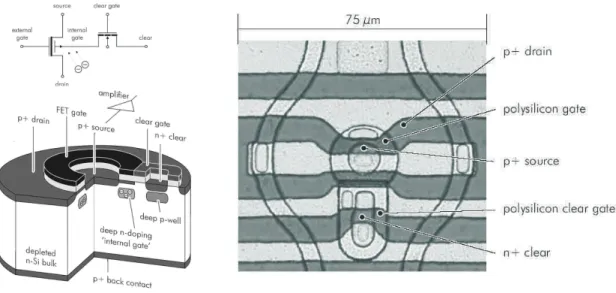
Figure 1. Cutaway view and microscope photography of a circular DEPMOSFET pixel. A pixel is made up of a circular p-channel MOSFET with attached clear region. The clear region consists of another MOS gate and an N
+-implantation, which from an additional ’parasitic’ n-channel MOSFET contacting the internal gate. The circular polysilicon gate has a width of 5 µm and a circumference of 47.5 µm. The respective representative circuit schematic is also shown.
A first prototyping production, PXD04, of DEPFET sensors including dedicated prototypes for XEUS was finished in 2003 at the MPI semiconductor laboratory in Munich, and the devices have been subject to extensive testing. A new prototyping production, PXD05, has been started recently and will be finished in early 2007. The excellent performance of the prototype devices from PXD04, which almost completely comply with the XEUS requirements in terms of noise, speed and energy resolution, have been reported elsewhere in detail. 3–6 The few minor drawbacks and problems discovered in the evaluation phase will be remedied in the new production by some modifications to layout and technology of the devices. In addition, steps towards a fully grown sensor were taken, and several large area sensors are included in the new production to allow for detailed studies of homogeneity and yield of the devices. Furthermore, the need for a more sophisticated front end electronics became more and more manifest, and concepts were developed to overcome the limits in terms of speed and noise set by the old front end (FE) electronics of the CAMEX type. The new FE electronics will implement trapezoidal shaping and will be tailor-made for both applicable readout schemes, source-follower readout and drain based current readout.
Here, the capabilities of the current DEPMOSFET devices will be briefly reviewed, before the key features and modifications of the next device generation will be discussed and design ideas and expected performance for the new FE electronics are shown. The DEPMOSFET structure can serve as a platform for a variety of new and interesting devices. For exemplification, results from structures implementing non-destructive-repetitive readout 7 (RNDR) are shown, which can easily be built using DEPFETs, the concept of macropixel detectors 8 and some other applications are briefly introduced.
2. DEPMOSFET DEVICES
A DEPMOSFET (DEpleted P-channel MOSFET) consists of a p-channel MOS-field effect transistor integrated
on the surface of a fully depleted, high resistivity n-type silicon bulk. 9 A potential minimum for electrons can
be generated underneath the device surface and can be enforced and confined in lateral direction to the area
below the transistor channel by an additional deep n-implantation. Bulk generated electrons are collected in
this potential minimum and their presence modifies the charge carrier density in the channel. Thus, the channel
conductivity becomes a function of the charge quantity in the potential minimum, which is therefore referred to as
internal gate. The internal gate persists regardless of the presence of a transistor current. If, however, the internal
V
SourceV
outI
ShuntV
GateR
fb +- V
DrainV
DrainV
outI
LoadV
SourceV
GateC
fbC
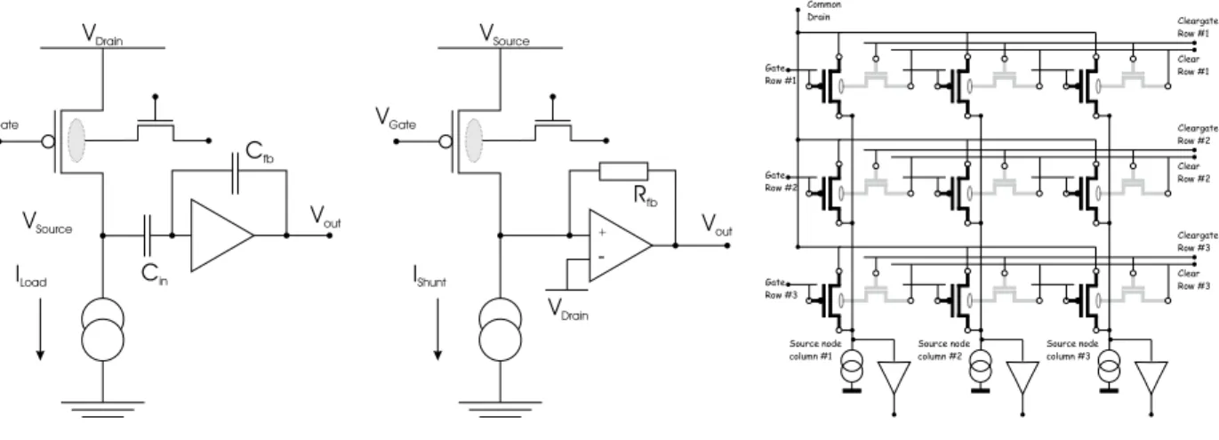
inFigure 2. Source follower (left) vs. drain based current readout scheme (middle). For the source follower readout, a constant load current is provided, and the DEPFET conductivity change is converted into a voltage step at the source, which can e.g. be amplified with an AC coupled voltage amplifier. For the drain based current readout, the conductivity change is converted directly into a current change, as all transistor terminal voltages are fixed, and the current change is evaluated by an I2U converter. To use the dynamic range of the I2U converter more efficiently, the pixel bias current is subtracted by a current source. Right: Arrangement and interconnection of pixels on a DEPMOSFET matrix prototype (simplified). The prototypes are designed for row-wise readout to ease control and readout. For source-follower readout, the pixels share a common drain contact. Gates, cleargates and clear contacts within one pixel row are connected together, while the pixel sources are connected column-wise. For drain based current readout, the role of drain and source can be exchanged, with the consequence of an inversion of pixel topology.
gate fills up completely, excess charge, and thus potential event information, can be lost to the nearest most positive contact. The accumulated charge therefore has to be removed regularly by applying a positive voltage pulse to the so-called clear-contact, an n + -doped region close to the internal gate, which is shielded towards the bulk by a deep-p implantation and towards the internal gate by a voltage-controllable barrier, the so-called cleargate. Clear and cleargate together can be considered as an additional n-channel MOSFET connecting clear and internal gate (see figure 1). The DEPMOSFET structures for XEUS have circular transistor geometry and have been designed for source follower readout. Here, the pixel source contact is biased by a constant current source; arrival of charge in the internal gate yields a voltage step at the source node which is proportional to the amount of charge collected. The charge information can be recovered by comparing the voltage levels at the source node of the pixel before and after the clear process. The relation between the charge in the internal gate and the resulting voltage step at the source node can be estimated to be:
∆V s = g q
g m · ∆Q s ,
where g m is the transconductance of the DEPMOSFET’s external gate, g q the so-called charge transconductance, which is the ratio
g q = δI pixel
δq int. gate
, (1)
and ∆Q s the amount of signal charge removed from the internal gate by the clear. In this scheme the readout speed is limited by the overall source capacitance, which, depending on the sensor array size, can be large. In combination with the intentionally low g m value of the DEPFETs, relative long source settling times may result.
An alternative scenario is the so-called drain based current readout, for which the transistor terminal voltages are fix and the change in the channel conductivity is directly converted into a current step, which is evaluated by means of a current-to-voltage (I2U)-converter connected to e.g. the drain terminal. In this case, the output voltage can be calculated by:
∆V out = g c · (g q · ∆Q s )
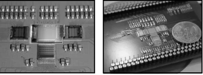
Figure 3. Left: Close-up of the central area of a hybrid, with the sensor (middle), the Clear switcher (right), the Gate switcher (left) and the CAMEX IC at the lower edge of the sensor. Right: Overview over a PCB type hybrid with the connector pins to the peripheral readout electronics and a coin showing the proportions.
where g c is the current-to-voltage conversion gain of the respective I2U-converter. The basic principle of the readout schemes is shown in figure 2.
To build large area sensors, a DEPFET pixel array is integrated onto a single die with common bulk and back contact. Groups of pixels can be formed and randomly accessed. A simple interconnection scheme has been chosen for the current DEPMOSFET structure prototypes, which is also shown in figure 2. Matrix readout is done row-wise and column-parallel. All pixels within one row integrate signal charges for a fixed time interval.
For readout, the transistor currents in the respective row are turned on, the voltage level at the source node is measured (signal level) and the clear operation is performed in the row. Next, the voltage level at the source node is measured again, now corresponding to the pixel signal with empty internal gate baseline level. The charge information can be obtained from the difference between signal and baseline level. Then, the row is turned off and the process is repeated in the next row.
The PXD04 XEUS DEPMOSFET matrix prototypes consist of 64 × 64 pixels of 75 × 75 µm 2 size. The device has a total sensitive area of 4.8 × 4.8 mm 2 and is integrated onto a 450 µm thick bulk. For the most favored structures, the circular transistor gate has by design a circumference of 47.5 µm and a nominal gate width of 5 µm. The drain contact is in the center of the pixel. The internal gate geometric size and doping concentration are dimensioned to store more than 10 5 electrons in a pixel, and measurements show that no deviation from linearity is observed up to that limit. For the current structures, g q -values of ≈ 200 - 300 pA / e − have been measured, depending on parameters like implantation profile, effective channel length and operating conditions.
The g q directly gives the amplification for drain based current readout. For source follower, the figure of merit is the source follower gain
g s = g q
g m
(2) expressed in µV signal step per e − charge stored in the internal gate. For the current structures, values of 3.7 - 4.8 µV / e − have been measured.
3. DEPMOSFET SENSOR INTEGRATION
For integration into a readout system, the matrix devices are mounted together with the required front end ICs
onto a hybrid carrier. Figure 3 shows photographs of fully assembled readout hybrids, a more detailed description
of the front-end electronics can be found elsewhere. 4 To control the row terminal voltages, the SWITCHER II
IC is used. This is a 64 channel, dual output, high voltage switching circuit manufactured in an AMS 0.35 µm
high voltage CMOS process. It has been specially designed for the purpose of DEPMOSFET matrix readout
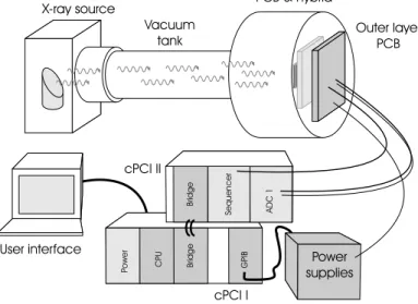
cPCI I User interface
Power CPU GPIBBridge
Power
supplies cPCI II
Bridge Sequencer ADC1
Multitarget X-ray source
Vacuum tank
Inner layer PCB & hybrid
Outer layer PCB
Figure 4. Simplified schematic of the VACDAQ readout system setup ,which permits measurements with a multitarget x- ray source inside a vacuum tank. Older measurements were made with a simpler version for tests inside a climatic chamber.
The system is controlled by a cPCI CPU. The sequencer card generates the control sequence, which is transferred via a digital interface to the hybrid support PCBs (inner/outer layer PCBs). They hold the hybrid and perform galvanic decoupling, level shifting, bias generation and filtering for the operation voltages. The analog output of the hybrids is transferred to the ADC card, which digitizes and formats the data, before it is stored on hard disk.
and provides two output ports for every channel, which can be toggled between two individual voltages each.
Facilities for precise timing of the switching process and easy integration of a large number of SWITCHER ICs make it a suitable device for building a daisy chain to read out large sensor arrays. The total switch voltage difference can be as large as 20 V. The analog front end IC used is the so-called CAMEX 64 G, a 64 channel parallel voltage amplifier using 8 fold correlated double sampling (CDS) and serial analog readout. A PMOS current source integrated in every channel biases the pixel columns. Typical operation currents are about 20 - 40 µA per column. Additionally, a built-in sequencer allows very flexible signal shaping schemes. The analog signal voltage information is read out using a sample & hold in combination with a serializer circuit.
Figure 4 shows a schematic overview over the peripheral readout system. A more detailed description has been given earlier. 4 The first measurements were made in a climate chamber using a table-top setup, the so-called LABDAQ setup; in the meantime, a more sophisticated readout system has been built to allow for measurements at variable X-ray energies within a vacuum tank (VACDAQ) using an x-ray multitarget source; both systems are based on the same architecture. The concept of both hardware and software is modular and scalable, so it can grow with increasing sensor sizes.
4. DEPMOSFET PERFORMANCE
In the following, measurement results on the baseline structure type showing the best performance are presented.
The device was illuminated with an 55 Fe source while being operated in a dried air atmosphere within a climate chamber at temperatures between +20 ◦ C and -60 ◦ C. Illumination took place from both front- and backside of the detector to study the effect of different widening of the charge cloud on the energy resolution. Measurements with variable X-ray energies inside the vacuum tank are currently under way.
The device was read out at a relatively low frame rate of about 300 Hz. Thus, the total signal and leakage current integration time for each pixel was about 3 ms. Hereby, the time used to actually perform the acquisition of the analog data within one pixel row was about 25 µs. The matrix pixels were operated at a pixel current of 25 µA, which provides for a mean pixel source follower gain of 4.2 µV / e − .
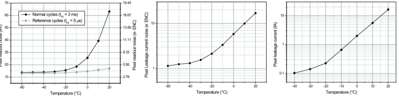
Figure 5 shows the temperature dependence of the device noise with (normal cycles) and without (reference
cycles) leakage current contribution. The device noise behaves as expected. The readout noise of the device
-60 -40 -20 0 20 1
10
PixelLeakagecurrentnoise(e-ENC)
Temperature (°C)
-60 -40 -20 0 20
10 20 30 40 50 60 70
2.78 5.56 8.33 11.11 13.89 16.67 19.44
Normal cycles (tInt= 3 ms) Reference cycles (tInt= 5?s)
Pixelreadoutnoise(e-ENC)
Pixelreadoutnoise(eV)
Temperature (°C)
-40 -30 -20 -10 0 10 20
0.1 1 10
Pixelleakagecurrent(fA)
Temperature (°C)
Figure 5. Dependence of total pixel noise (normal cycles) and readout noise (reference cycles) on device temperature (left). The total noise is the standard deviation of the offset values of that pixel, while the readout noise is measured with an additional clear in advance removing the integrated leakage current. With these values, the leakage current contribution to the total noise (middle) can be extracted. By subtracting the offset maps, the pixel leakage current and its temperature dependence (right) can be measured directly. As expected, the leakage current shows an exponential dependence on temperature down to a temperature of -20
◦C. Below that limit, measurement accuracy is limited by the intrinsic noise of the readout system.
at room temperature is as low as 4.7 e − ENC, which is in good agreement with the expectation from CAMEX filter function and DEPMOSFET noise power spectrum (see figure 8). With decreasing temperature the noise also decreases to a level of 3.5 e − ENC due to the decrease of series noise within the pixel MOSFET and the CAMEX. As expected, the measured leakage current contribution itself shows an exponential behavior down to a temperature of -20 ◦ C, where the readout noise becomes dominant and the leakage current contribution can not be precisely extracted. The pixel leakage current can also be measured directly (see figure 5), which shows the expected exponential behavior down to a temperature of -20 ◦ C. Below this limit, the measurement again is limited by the intrinsic readout noise of the front end chain. At room temperature, a mean pixel current of 16.5 fA / pixel is measured, corresponding to a current of 285 pA / cm 2 . The leakage current dispersion is about 1 fA and the distribution is homogeneous over the device area.
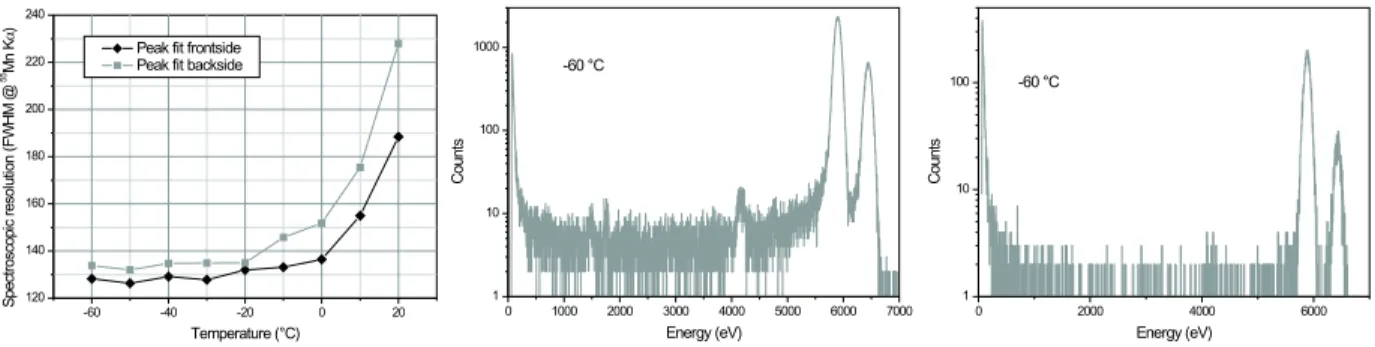
The spectral resolution of the devices is calculated by determining the width of the 55 Mn-Kα-peak in the singles spectrum (i.e. no charge sharing between pixels) for the given temperature. Figure 6 shows the dependence of the spectral energy resolution on the device temperature. As expected, the spectral resolution improves with decreasing temperature as the total noise decreases. The energy resolution becomes as good as 127 eV for the frontside illumination and 133 eV for the backside illumination. Additionally, some examples for 55 Mn spectra taken at -60 ◦ C are shown for frontside (figure 6, middle) and backside ( figure 6, right) illumination. The spectra for backside illumination show a much better peak to background ratio, as the background for frontside illumination is dominated by partials caused by the dead layers on top.
Subtracting the Fano noise contribution, one yields ENC values for the specral energy resolution of 4.9 e − ENC for frontside illumination and 6.6 e − ENC for backside illumination. This discrepancy between the spectral resolution and the total noise of only 3.5 e − can be explained by taking data analysis artifacts into account, as the adaption of the analysis algorithms to the special needs of DEPMOSFET pixels is at a relatively early stage. Also still under investigation is the large discrepancy between the energy resolution measured for the frontside and the backside illumination. Possible explanations are differences in charge collection between front- and backside illumination, which might influence the determination of gain, threshold effects or analysis artifacts.
In addition to readout noise and spectral resolution, a variety of other DEPMOSFET structure related effects
has been studied, which directly affect the performance on fields like low energy background, readout timing
behavior and peak-to-background ratio. The effects are discussed more in detail elsewhere 5 ; the found remedies
are discussed in the following section.
-60 -40 -20 0 20 120
140 160 180 200 220 240
Peak fit frontside Peak fit backside
Spectroscopicresolution(FWHM@55MnK?)
Temperature (°C)
0 1000 2000 3000 4000 5000 6000 7000
1 10 100 1000
-60 °C
Counts
Energy (eV)
0 2000 4000 6000
1 10
100 -60 °C
Counts
Energy (eV)
Figure 6. Dependence of measured spectral resolution at the
55Mn-Kα-peak on the device temperature. Given are the values in eV FWHM (left) and two examples for spectra measured at -60
◦C. Not much change is seen below -20
◦C.
The energy resolution becomes as good as 127 eV FWHM for frontside illumination (middle) and 133 eV for backside illumination (right).
5. THE NEW PROTOTYPES
The new production of DEPMOSFET sensor prototypes for XEUS has three main targets. First, the feasibility of large-area prototypes will be demonstrated by the production of a variety of large area sensors, which will also permit extensive yield and homogeneity studies. Secondly will new device and structure ideas be tested on single pixel prototypes and small area devices for their performance and suitability for future large area sensors, and thirdly will the observed minor drawbacks and problems of the first production be remedied by a variety of modifications in the production technology. Compared to the number of design variants for PXD04, the number of designs could be significantly reduced, as a number of variants were ruled out. For the remaining design options, two main objectives were aimed at. These were to further facilitate complete clear and to prevent charge loss occurring for some of the design variants.
A complete clear with low usage of clear resources (i.e. clear time and clear voltages) is highly desirable, as this ensures high-speed operation with good noise and energy resolution. In PXD05, this will be achieved by modifications to the implantation profiles underneath the cleargate and by improved accuracy in lithography preventing local potential minima in the internal gate, which introduce a time-depending component to the clear characteristics. These modifications will not affect g q or charge handling capacitance.
Charge loss can be observed only for devices with the source contact in the middle of the pixel. Unfortunately, this design option is highly favorable, as it eases pixel interconnection on the matrix a lot. This, in turn, provides for increased routing resources for other purposes like, for instance, forming of ROIs. The charge loss is caused by a lack of drift field underneath the cleargate, so charges get stuck there and are removed by the next clear and their information is lost. Therefore, this situation can be prevented by introducing a drift field in the critical region, which is also done by modifying the shape of the implantations underneath the clear.
In addition to the design modifications discussed above, progress in manufacturing equipment and handling experience has been made, and considering the extremely good yield numbers (> 90%) of the PXD04 productions, good yield is to be expected from PXD05 even for the large area devices.
Most of the design variants and their permutations are produced in the standard (XS) format, which has 64 x 64 pixels. A number of selected and promising design variants will be implemented on larger devices with 256 x 256 (XL) or 128 x 512 (XXL) pixels. The XL device comes in single sided and double sided readout versions, the latter is used for high frame rate readout tests. The XXL variant emulates one sector of the final XEUS WFI and will be used for yield and homogeneity tests, and, as well, for high speed readout tests. Figure 7 shows the sensor formats and their relative sizes. The respective active areas are shown in white.
6. ADVANCEMENTS IN FRONT-END ELECTRONICS
The speed requirement for the final XEUS instrument demand improved performance of the respective readout
electronics. The performance of the existing ASICS in terms of speed is not sufficient, and therefore improved
Figure 7. The sensor device sizes for PXD05 (white: active area) and required readout electronics start with the standard prototype size (XS) of PXD04 (second left), which has 64 x 64 pixels and an active area of 4.8 x 4.8 mm
2. It is read out by one 64 channel readout IC (white) and 2 Switchers (grey). The new large area prototypes (XL, middle positions) have 256 x 256 pixels and an active area of 19.2 x 19.2 mm
2. Readout is done by 2 128 channel readout ICs and 8 Switcher ICs. A second XL device format is read out to both sides in parallel, requiring twice the number of readout ICs. The XXL prototype (right), with 512 x 128 pixels, has the full size of a XEUS WFI sector and will be used for speed tests and yield monitoring.
0 1 2 3 4 5 6 7 8 9 10
2 3 4 5 6 7 8 9 10
Weighting Function Total Width [µs]
ENC [electrons]
Flat-top=0 (Triangular) Flat-top=0.2µs Flat-top=0.5µs Flat-top=1µs
10 100 1000 10000 100000
Frequency [Hz]
1E-024 1E-023 1E-022 1E-021 1E-020
A2/Hz
Circular 5u 30uA 60uA 120uA 240uA
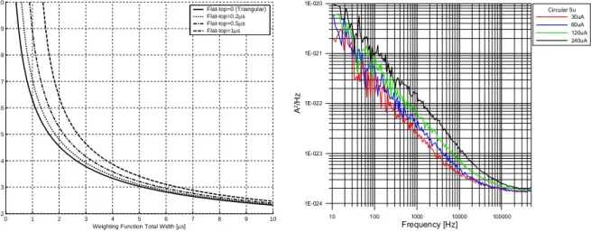
Figure 8. Noise power spectrum of a DEPMOSFET pixel (right) and the resulting simulated readout noise assuming trapezoidal shaping with varying flat top width (left). The target total weighting function width for XEUS is about 4 µs. It can be seen, that a shorter flat top improves the noise performance, thus fast clear is beneficial. The noise power spectrum of the DEPFET device is still not yet fully understood and subject to intense studies.
CAMEX devices dedicated to source follower readout and implementing 8-fold CDS will be built with 64 and 128 channels each. An improved, faster output buffer will provide increased speed for the analog output serializer;
a built-in bandwidth limitation will allow adaption of the analog bandwidth to the respective readout time and alterations in the amplifier structure will provide for an improved linearity.
As can be shown, the optimum filter with respect to white series noise is the triangular filter; and the multiple
CDS filter performs best, if it is used to approximate triangular filtering, e.g. by an appropriately adjusted
bandwidth. As, however, the DEPFET device needs a finite time at the peak of the weighting function to
perform the clear process, the optimal filter for DEPFET structures is the trapezoidal filter, the triangular
filter with a finite flat top. Figure 8 shows an example for measured noise power spectra for PXD04 DEPFET
structures for various currents. From the noise power spectrum, the expected resulting readout noise applying
trapezoidal shaping with varying flat top width is calculated. The simulation shows, that for the measured noise
power spectrum the resulting readout up of total weighting function width ( ≈ 4 µs) is well between 3 and 4 e −
ENC. An IC showing that performance together with a DEPFET device would mark an important step towards
V2I
DEPMOSFET pixel Bias current
source
First stage amplifier
Current to voltage converter
Integrator stage Subtraction stage
To readout node / output multiplexer
Source
Gate
Drain
Integrator stage DEPMOSFET
pixel
Offset current subtraction
Subtraction stage
To readout node / output multiplexer Source
Gate
Drain
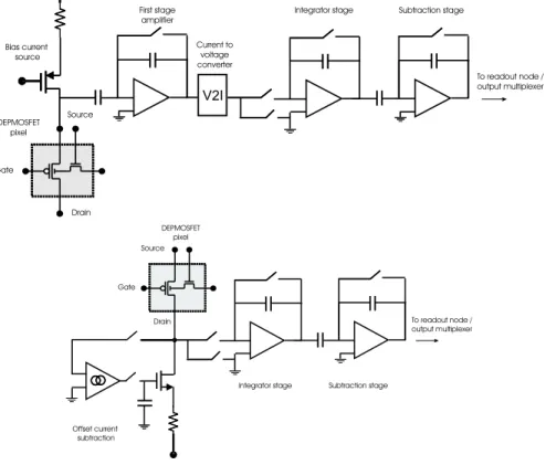
Figure 9. Block diagrams of a channel of the new readout electronics for XEUS. Both devices implement trapezoidal filtering by the use of a combination of integrating and subtraction stages. The source follower device (left plot) uses an AC-coupled first stage amplifier and a current-to-voltage converter as an interface to the integrator, the current-based drain readout device has a low-noise current subtraction stage at the input to subtract the pixel’s offset current.
the targeted XEUS performance.
Therefore, concepts are currently being developed to implement trapezoidal shapers within an IC for DEPFET device readout, and two different FE solutions are being designed. In both cases, the shaping will be implemented by means of current integrating and subtraction stages. One of the designs will be dedicated for drain-based current readout and will directly integrate the current provided by the pixel device; to use the amplifier’s dynamic range more efficiently, the offset current of the pixel is subtracted prior to signal acquisition. The other design will feature the source follower, using the same shaper, but a combination of a first stage amplifier and a current- to-voltage converter for interfacing source follower and shaper. Block diagrams of the two structures are shown in figure 9.
In addition to the efforts in improving the filtering performance of the front end electronics, the studies of the DEPFET noise spectrum, which shows some anomalous characteristics, will continue. As can be seen in figure 8, the series noise floor beyond the corner frequency only slightly depends on the current and is also higher than the series noise expected from the transistor characteristics. These effects will be studied in detail, as any improvement made here will directly impact heavily on the noise performance.
7. REPETITIVE NON-DESTRUCTIVE READOUT
In addition to the standard application as a building block for a large-area imager sensor, several alternative
applications of the DEPFET structure have been discussed for a couple of years. 10 Especially the feature of
repetitive non-destructive readout (RNDR), where the same amount of charges can be repetitively measured
arbitrarily often, is of interest for applications, in which low intensity photon signals have to be detected with
Transfer- gate
Readout- node 2 Cleargate/
Clear Common
bias Gate 2
- Gate 1
node 1 Readout-
Gate 1 Gate 2
Transfer-
gate Clear Cleargate
Internal gate
Global HE Transfer-
region Common
bias
Readout node 1
Readout node 2
Figure 10. Cutaway and circuit schematic of a DEPMOSFET RNDR superpixel based on the XEUS topology. A superpixel consists of two DEPMOSFET subpixels, one of which is equipped with a clear structure. Charge is transferred between the two subpixels’ internal gates with the help of the transfer gate contact. A global deep-n implantation defines the transfer channel and prevents charge loss due to trapping at the interface. The outer bias contact is common for both subpixels, the individual readout nodes for the subpixels are the contacts inside the gate electrode rings.
high sensitivity, but less demanding time requirements, but, with an increased speed, also for high-speed, low occupancy X-ray imaging spectroscopy detectors. Structures based on the RNDR principle provide a reduction of series noise, both white and 1/f, and ENC values below 1 e − are possible. First RNDR structures based on floating gate and floating diffusion amplifiers were successfully tested for CCD readout several years ago. 11 Main problem here were the very the long readout time and relatively low device operating temperatures to reduce the influence of thermally generated charge carriers.
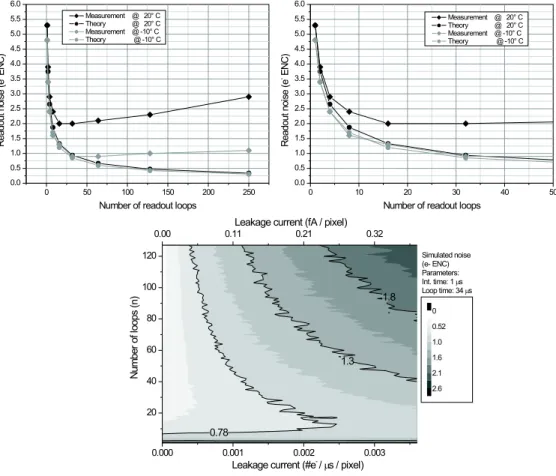
RNDR single pixel structures and small 4x4 pixel matrices can be built easily using DEPMOSFETs, prototypes have been included in the PXD04, and tests on single pixels with XEUS topology have successfully been started, the results are encouraging. Figure 10 shows cutaway and circuit schematic of a RNDR pixel based on circular topology. The charge can be transferred between the internal gates of the two DEPMOSFET subpixels with the help of the transfergate contact, and the transfer has the same effect as the clear for an ”ordinary” pixel, but with preservation of the signal charge. A global deep-n implantation keeps the transfer channel in the depth of the silicon, thus preventing charge loss due to trapping at the interface. Figure 11 shows first measurement results of readout noise vs. number of transfer cycles measured at different temperatures. In theory, 12 the readout noise is expected to decrease with the square root of the number of iterations, a transfer cycle followed by a measurement, as the series noise contributions are averaged out. In practice, however, a deviation from the 1/ √ n behavior is observed, which is most likely caused by the effect of leakage current electrons arriving during the shaping process, thus distorting the noise distribution. This assumption is confirmed by Monte-Carlo studies of the influence of leakage current and the number of readout iterations on the observed noise performance. As observed in the measurements, an optimum number of iterations can be found for a given level of leakage current, for which the lowest noise is observed. Quantitative studies of this effect are currently under way.
The first results on DEPFET based RNDR devices are very promising. Measurements on the existing devices and small matrices will continue, and the setup will be further improved. Some improved layouts of single pixels and small matrices are also implemented in PXD05. For the current devices, a readout noise as good as 0.6 e − ENC has been observed for a number of 32 readout iterations at a temperature of -15 ◦ C for iteration times of 32 µs. Below a readout noise of 0.3 e − ENC it will be possible to determine the number of single electrons integrated with > 90 % sensitivity, making RNDR DEPFET based detectors a promising concept for future applications, e.g. low intensity photon detectors. But RNDR devices are also of interest for XEUS: Sufficient routing resources provided, an RNDR pixel array could even be implemented on the XEUS WFI, e.g. in a central ROI, and, depending on the intensity of the observed objects and available readout time, be used for certain observations.
8. ALTERNATIVE APPLICATIONS
DEPMOSFET based matrix devices can be built with a wide range of pixel sizes. DEPMOSFET pixel arrays
with a pixel size of below 30 µm × 30 µm have been built applications in high energy physics. 13 The current
concept of the XEUS WFI requires a pixel format of 78 µm × 78 µm. And the DEPMOSFET’s low noise
0 50 100 150 200 250 0.0
0.5 1.0 1.5 2.0 2.5 3.0 3.5 4.0 4.5 5.0 5.5 6.0
Readoutnoise(e-ENC)
Number of readout loops Measurement @ 20° C
Theory @ 20° C
Measurement @ -10° C Theory @ -10° C
0 10 20 30 40 50
0.0 0.5 1.0 1.5 2.0 2.5 3.0 3.5 4.0 4.5 5.0 5.5 6.0
Readoutnoise(e-ENC)
Number of readout loops Measurement @ 20° C
Theory @ 20° C
Measurement @ -10° C Theory @ -10° C
1.3
0.78
1.8
0.000 0.001 0.002 0.003
20 40 60 80 100 120
0.00 0.11 0.21 0.32
Leakage current (fA / pixel)
Leakage current (#e
-/ ?s / pixel)
N u m b e r o f lo o p s (n )
0 0.52 1.0 1.6 2.1 2.6 Simulated noise (e- ENC) Parameters:
Int. time: 1?s Loop time: 34?s