1
A clustering engine for data rate reduction in the Belle II pixel detector
Andreas Wassatsch,Member, IEEE, Sven Herrmann, Rainer H. Richter and Ladislav Andricek, Member, IEEE
Abstract—The DEPFET technology has been chosen as the baseline for the vertex pixel detector of the Belle II experiment at KEK\Japan. This detector consist of22modules, each proposed to be equipped with 2×250×512 pixel. With the proposed average readout frequency of 10kHz and 30kHz peak rate a huge data stream of approx. 100Gbit/s will be generated. To reduce this data stream to a more feasible value, we have to take advantage of the low occupancy of approx.1−2%and the the hit distribution within the pixel array. For this purpose a pipelined clustering algorithm was developed, which can handle cluster sizes of 3×3 or 5×5 at full readout speed. These algorithm can handle data from non bricked sensors and also from bricked designs. It is able to reduce the data rate by up to 50%. The collection of the clustered data packages from the row wise parallel pipeline are controlled by a specially developed output scheduler, which assures together with the corresponding FIFO structures the data-handling capability. In this paper we will present the overall structure of such a DCE (Data Clustering Engine) and also the details of the implemented clustering and output scheduling algorithms. Furthermore the impacts of the constraints on speed, power and area on the developed circuit and the chosen realization given by the experiment environment will be discussed in detail.
Index Terms—Belle II, DEPFET, clustering algorithm, lossless data compression.
I. INTRODUCTION
THE Belle detector is part of thee−e+asymmetric-energy collider KEKB at the High Energy Accelerator Research Organisation (KEK) in Tsukuba (Ibaraki Prefecture, Japan), which is one of the world’s highest luminosity machines.
These multilayer detector is characterized by a large solid angle coverage and a high precision vertex location in the range of some tens of micrometers.
The increased requirements on the detector systems of the Belle experiment driven by the ongoing upgrade of the KEKB accelerator for a two orders of magnitude higher luminosity leads to a redesign of serveral subdetector systems. For that purpose also the central vertex detector system has to be further developed for the Belle II experiment.
A. The DEPFET vertex detector for the Belle II
As the central part of the Belle II detector the vertex pixel detector has to deliver the necessary information for a high
Manuscript received Nov. 13, 2009.
A. Wassatsch and R.H. Richter and L. Andricek are with Max-Planck- Institut f¨ur Physik, F¨ohringer Ring 6, 80805 M¨unchen, Germany and with MPI Halbleiterlabor, Otto-Hahn-Ring 6, Geb. 72, 81739 M¨unchen, Germany (email:wassatsch@hll.mpg.de).
S. Herrmann is with Max-Planck-Institut f¨ur extraterrestrische Physik, Giessenbachstrasse, 85748 Garching, Germany and with MPI Halbleiterlabor, Otto-Hahn-Ring 6, Geb. 72, 81739 M¨unchen, Germany.
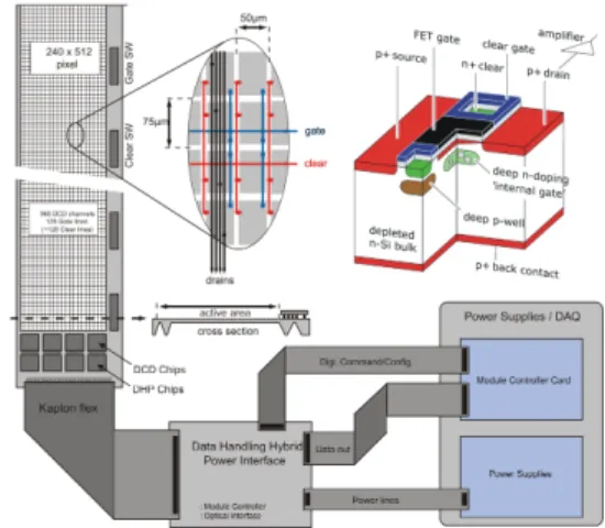
precision location of the vertex of anye−e+ collision at these interaction point. Due to the high expected background level the architecture of the vertex detector has to be adapted to the increased data rates. Therefore the DEPFET [1] technology has been chosen for the baseline design of the new vertex detector for the Belle II experiment. The detector subsystem themselve will be consist of two layer of in total 22 ladders, very close mounted around the beampipe. On the balcony of these thinned ladders the DEPFET Current Digitizer (DCD), the Data Handling Processor (DHP) and the corresponding Switcher (SW) ASIC’s has to been placed, like shown for a half ladder in Fig. 1. For the readout each half ladder will be processed independently. All of these ladders will be equipped with an 2×240×512 DEPFET pixel array. The ladder will be thinned in the area of the detector array to a thickness of 50µm.
Fig. 1. Belle II vertex detector princip
Steared by the DHP, the Switcher ASIC’s drive the Gate and Clear signals of the DEPFET matrix. The DCD then digitize the readout current of four DEPFET rows in parallel and send via local serial links the digital values to the DHP. In the first phase here only a zero-suppresion will be executed to realize a necessary data volume reduction. These data then will be send via a flex cable to the Data Handling Hybrid (DHH), from where they then would be optical transmited to the of detector data aquisition system. On the DHH also the local power conversion for the supplies of the ladder ASIC’s will be performed. Due to the fact, that the pixel vertex detector for the Belle II experiment will generate a data stream, which is more than one order of magnitute higher as the total amount of data generate by all other subdetector systems of the experiment a further data rate reduction is clearly necessary.
2
B. Lossless data compression
With a frequency of 50M Hz at row level the readout of one side of a ladder will generate a datastream of 96Gb/s respectively15Gb/safter zero-suppression under the assump- tion of 5% occupancy. The dimension of a single DEPFET pixel are designed in a way, that every event doesn’t exceed a cluster of3×3pixel, which was verified by event simulations.
With that previous knowledge about the data distribution in the pixel matrix, it is possible to develop a lossless data compression scheme via a simple recoding of the geometric address information for a 3 × 3 pixel cluster. Instead of transmission of the whole x/y coordinates of every pixel, we will transmit only once the full x/y value of a 3× 3 matrix together with a smaller local address information for each pixel. By utilization of these coding scheme a lossless data rate reduction up to a factor of two are achievable, like shown in equ. 1.
c= n(log2(X) +log2(Y) +Vadc)
log2(X) +log2(Y) +nVadc+ (n−1) (1) The coding scheme already starts to save bits with a pixel cluster count of n = 2. Only for single pixel constellation (n= 1) we will see a penality of up to35%, which we have to pay there for the recoding scheme.
II. IMPLEMENTATION
TO take use of these data rate reduction scheme, the clus- ters has to be determined in realtime on the data handling processor. A possible solution for that will be presented in the following part of these article.
A. Clustering algorithm
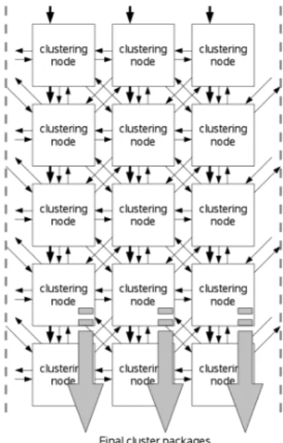
We implement the clustering algorithm for a3× 3cluster pixel configuration. Nevertheless the algorithm can also be used for 5× 5 cluster or bricked pixel designs. The massive parallel clustering algorithm implementation use only the direct neighborhood relations to the surrounding pixels of a node, like shown in Fig 2. To further simplify the development process an array of identical clustering nodes will be used, where a node directly correspond to a single pixel. By the time-multiplexed readout of the pixel matrix in theY direction, the dimension of clustering node array can reduced to a5×X configuration for a 3×3cluster design.
These hardware structure proceed the clustering algorithm in one clock cycle per row as follows:
• Spread the data valid flag to all neighbors, only in the case these pixel wasn’t attracted by an earlier iteration
• Collect the data valid flag from all neighbors and spread these count value again to all surrounding nodes
• Determine, if the local count value is the highest value and try to attract the corresponding neighbor pixel
• In case of multiple attraction, the node of a attracted pixel has to decide on a geographical rule to which center it will belong
• Send and store the corresponding tag flag
Finally the pixel data of detected clusters has to been collected at the end of the pipeline. These algorithm is char- acterized by a very small number of interconnections between the nodes and a identical hardware structure in all stages.
Fig. 2. Clustering pipeline array
B. Output scheduler
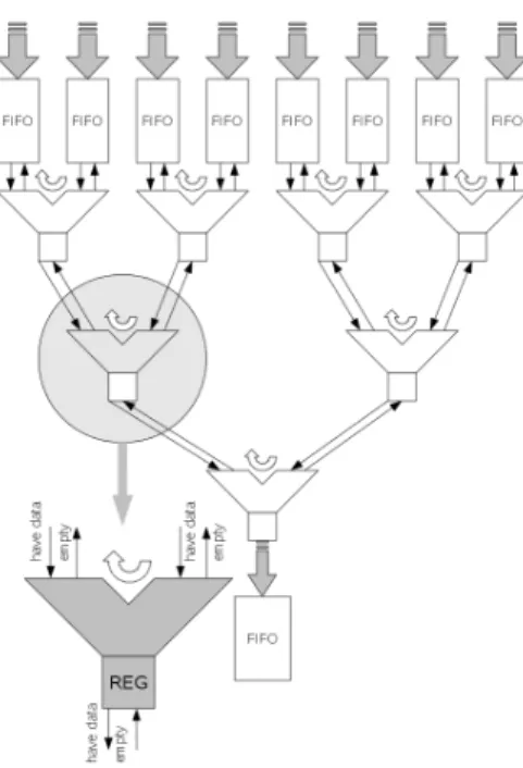
As random as from the system view the readout data, delivered by the multi-channel analog digital converter ASIC DCD, are distributed also the determined clusters will come out from the pipeline. Therefore a unit, which collects the cluster data packages, is needed. To prevent long or complex daisy-chain structures, as used in many other implementations, a binary tree configuration (Fig. 3) together with a local round robin scheduler strategy has been chosen, to form a single data package output stream out from the240possible drivers. Each node is able to store one cluster package and to communicate with the preceding and succeeding nodes in the tree to steer the package propagation. The simple construction of such a node allows a higher operating speed then daisy-chain based architectures. Furthermore the tree design can be easily scaled up for a increased input channel count.
The dimension of the in- and output FIFO’s depends on the cluster data distribution, the cluster density and the final readout speed. For the proposed application with the current requirements the input FIFO stage can be reduced to a simple register structure, which can store only one cluster package. In the test chip design the FIFO is sized for 16 cluster packages, to be able to handle also higher package rates as needed in our current application. These FIFO’s can also be used for testing the scheduler themselves, by external filling with package data via the slow control interface.
3
Fig. 3. Output scheduler tree architecture
C. DCE test chip architecture
To prove the concept and the performance of the algorithms and also to decouple the development of the DHP unit from the clustering unit, the clustering engine is in the first phase of the project implemented within a separated ASIC in a 90nm process technology. In a second phase both units will be merged into a final data processing unit, which has to fit on the balcony of the thinned DEPFET detector module (Fig. 1).
The DCE has to house therefore in the first phase additional components for the interface to the DHP circuit, like shown in Fig. 4. Because of the scrambled output data stream of the first phase DHP, the orignal multi-channel parallel datastream output of the DHP zero-subpression unit has to be rebuild locally on the DCE. For these purpose a deserializer and a multipage memory together with the corresponding demultiplexer are implemented. By an slow control access interface to a SPYIN component in the deserializer and to the emulated dual-port memory different artificial tests on these data stream input interface could be evaluated. In the first phase the serial connection between the DHP and DCE could be realized by a less demanding off chip driver with reduced power consumption, because they are located in the test setup only in a short distance. These additional circuits will be obsolete in the merged device.
The die area of the standalone DCE is mainly determinate by the size of the In- and Output- FIFO structures and the fully parallel implemented cluster pipeline. An integration of the with the DCE chip tested clustering pipeline on the DHP will increase the die area by approximately30%of the current phase one concept. For slow control operation and module interconnection verification a standard JTAG interface, like in the others application specific devices on the module, are implemented. This interface allows an access to almost all
memory structures for functional debugging purposes.
Fig. 4. General test chip architecture
D. Implementation details
As a first step for the DCE implementation we use a 8 channel version (5.1 × 1.65mm2) to prove the clustering concept (Fig. 5). At the same time it is also our first test chip to become familiarly with the new technology and design-kit at a lower cost. A second test chip is planed with a 40/64 or 240/256 column implementation depending on the final DCD/DHP configuration.
Fig. 5. DCE8 layout
Due to the implemented SPY/STIMULI units in the seri- alizer and de-serializer circuit and almost all via the JTAG interface accessible memory fields, the DCE chip can be fully independently tested.
The layout of the clustering node is build up from a custom made standard cell library. The current implementation needs 800×50µm2die area and consumes less than1mW per node at 100M Hz test frequency. A complete clustering pipeline with 240 channels fullfill with a power consumption of less than1 W under the experiment condition the defined design requirements. We has to design the node with a unusual shape, where one dimension is very narrow in respect to the second, due to the fact that the pipeline could not be divided into two
4
parts and so the whole pipeline has to fit with the 240 channels in parallel to the balcony of the detector.
To improve the relaibility of the asic, all register cells are based on the in the ASTEROID64 project [2] already proven modified DICE [3] cell architecture without any drawback in respect of area, timing and power compared to the commercial standard cell library devices.
Driven by the limited die area and the high amount of memory, which is needed for the FIFO’s, standard SRAM building blocks out from a commercial SRAM compiler [4]
[5] are used to realize the memory fields. The SPY blocks are implemented as a dual port memory. Due to area limitations a two bank single port memory solution was chosen for the FRAME FIFO. All SRAM ip blocks are checked via additional parity bits to detect possible data corruption in the application.
The clustering array can be placed in the final DHP chip directly after the zero-suppression unit and before the output scheduler with an overhead of14×5mm2 for a 240column implementation.
E. Test plan and environment
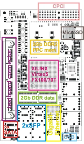
The first phase of the DCE 8 channel asic tests is assigned to standalone function verification of the ASIC. For that purpose a dedicated hybrid board will be directly connected to our general purpose test and data aquisition board IGEL (Fig. 6).
Over that connection a emulated JTAG interface to the ASIC will give the full control to all the implemented memory blocks of the DCE8 and the possibility to pre-load any pattern into the SPYIN or FRAME FIFO’s.
In a second step, the FPGA on the IGEL board will be used to emulate the DHP data stream and also readback and prove the DCE8 output data stream.
In a second phase the DCE8 will be directly connected to the DHP to further check the clustering engine in the final environment with real DEPFET matrix data.
III. CONCLUSION ANDOUTLOOK
WE have developed the first generation of a realtime clustering chip for data rate reduction of the DEPFET vertex detector in the Belle II experiment. The implementation shows the possibility of an hardware based approach for clustering pixel detector data in a very early stage of the signal processing flow in the direct neigborhood of the digitizer and readout circuits. Now the functional test on the real devices has to prove the promising results from the circuit simulations.
After the functional verification of the DCE8 a redesign of the clustering array will focus on area and power reduction by optimization of the node elements.
REFERENCES
[1] J. Kemmer and G. Lutz, “New semiconductor detector concepts,”Nucl.
Instr. and Meth. A, vol. 253, pp. 365–377, 1987.
[2] M. Porro, L. Brombelli, G. D. Vita, C. Fiorini, S. Herrmann, G. Segneri, L. Str¨uder, J. Treis, A. Wassatsch, and S. W¨olfel, “Asteroid: a new 64 channel asic for source follower based readout of the mixs depfet arrays on bepicolombo,” inNuclear Science Symposium Conference Record, NSS 2007, vol. 3. IEEE, Oct. 26.- Nov. 3 2007, pp. 2392–2397.
Fig. 6. IGEL board
[3] M. N. T. Calin and R. Velazco, “Upset hardened memory design for submicron cmos technology,”IEEE Trans. Nucl. Sci., vol. 43, no. 6, pp.
2874–2878, 1996.
[4] IBM 90nm CMS9FLP HVT LVT METRO- RAM-SP Datasheet, ARM Limited, 2009, version 2009Q2V1.
[5] IBM 90nm CMR9FLP HVT LVT METRO-RAM-DP Datasheet, ARM Limited, 2009, version 2009Q2V4.