Optimization of the new Pixel Vertex Detector for Physics Running in the Belle II Experiment
Optimierung des neuen Pixel Vertex Detektors f¨ ur die physikalische Datennahme im Belle II Experiment
Masterarbeit aus der Physik
Vorgelegt von Markus Reif September 13, 2019
Fakult¨ at f¨ ur Physik
Ludwig-Maximilians-Universit¨ at M¨ unchen
Abstract
B-factories like the PEP-II asymmetric energy electron-positron collider with its detec- tor BaBar and KEKB with the Belle detector impressively confirmed Kobayashi’s and Maskawa’s theory of CP violation within the Standard Model, in particular concerning the large CP violation expected for B mesons decays. However, there are still tensions in some measurements and, most importantly, the observed CP violation is by far not sufficient to explain the observed asymmetry of matter and antimatter in the universe.
Clearly, new physics beyond the Standard Model is needed.
Therefore, the KEKB collider and the Belle detector, located at the High Energy Acceler- ator Research Organization KEK in Tsukuba, Japan, were upgraded to SuperKEKB and the Belle II detector in the past years. The goal is to search for new physics by hopefully measuring significant deviations from the Standard Model. This is achieved by increasing the luminosity by a factor of 40 compared to KEKB. The design goal of SuperKEKB is a peak luminosity of 8×1035cm−2s−1 and an integrated luminosity of 50 ab−1 until 2027, almost two orders of magnitude more then collected by Belle.
To cope with this tremendous increase of data rate also the detector was upgraded from Belle to Belle II. One of the main upgrades was the installation of a two-layer silicon pixel detector (PXD), based on the DEpleted P-channel Field-Effect Transistor (DEPFET) technology, as innermost detector, which is crucial for the precise measurement of CP violation observables.
The Belle II detector started taking data in March 2019 and already showed the remarkable performance of the PXD, which was developed and is commissioned under the leadership of several German institutes.
However, there are still a lot of ongoing efforts for example in software development for ease of operation of the PXD. Furthermore, hardware tasks continue to complete or possibly exchange the PXD, since currently only half of the foreseen modules are installed.
This thesis contains two main parts. In the first one it describes the development of a new software system, which aims to speed up the complex calibration procedure of the roughly 8 million pixels in the PXD detector. The method is explained and results at different test sites (MPP and DESY) are shown.
The second part deals with an important step in the production of the PXD ladders, which is the gluing of ladders. The gluing connects two modules to a ladder, being large enough to cover the required acceptance region of the Belle II detector. The original gluing procedure had severe yield problems, thus a new one was developed. This thesis outlines both procedures and the results of the first ladders, which were glued with the improved procedure, are shown.
Contents
1 Introduction 7
2 Theoretical Background 11
2.1 The Standard Model . . . 11
2.2 Discrete Symmetries . . . 12
2.2.1 Parity . . . 13
2.2.2 Charge Conjugation . . . 13
2.2.3 Time Reversal and CPT-Theorem . . . 13
2.3 Violation of Symmetries . . . 14
2.3.1 Parity Violation . . . 14
2.3.2 CP Symmetry . . . 14
2.3.2.1 The Cronin and Fitch Experiment . . . 15
2.3.3 Types of CP Violation . . . 18
2.4 Theoretical Description of the SM and the CKM matrix . . . 19
2.5 The B-factories BaBar and Belle . . . 23
3 SuperKEKB and Belle II 25 3.1 The SuperKEKB Accelerator . . . 25
3.2 The Belle II Detector . . . 25
3.3 Vertex Detector VXD . . . 26
3.4 Central Drift Chamber CDC . . . 27
3.5 Time-Of-Propagation TOP counters . . . 28
3.6 Aerogel Ring-Imaging Cherenkov ARICH detector . . . 28
3.7 Electromagnetic Calorimeter ECL . . . 29
3.8 Solenoid Magnet . . . 29
3.9 KL and µdetector KLM . . . 30
4 Pixel Vertex Detector 31 4.1 DEPFET . . . 32
4.2 ASICs . . . 33
4.2.1 Switcher . . . 34
4.2.2 DCD . . . 34
4.2.3 DHP . . . 34
4.3 PXD Modules and their Readout . . . 34
4.4 Off-Module Electronics . . . 35
5 Tests and Characterization of PXD Modules 39
6 Pre-Offset VNSubIn Adjustment 43
6.1 Motivation . . . 43
6.2 Method . . . 43
6.2.1 Additional Features . . . 45
6.3 Results . . . 46
6.3.1 Test at the MPP DHE system . . . 47
6.3.2 Test at the DESY DHH system . . . 47
6.4 New Implementations . . . 47
7 Ladder Gluing 53 7.1 Original Procedure . . . 54
7.2 Improved Procedure . . . 55
7.2.1 Gluing of the first ‘hot’ Ladders . . . 56
8 Conclusion and Outlook 61
1 Introduction
Why is there only matter and no macroscopic accumulations of antimatter in our universe?
This is one of the most fundamental question of nature, and still yet not answered. The Big Bang theory proposes that the universe was ‘born’ about 13.8 billion years ago out of an infinitely dense and hot state. During this event everything was created: space, time, energy and matter. Based on hard experimental facts from high energy physics, the Big Bang model asserts that matter and antimatter were created in equal amounts.
Since a particle and its antiparticle annihilate into energy, i.e. photons, there should only be radiation in the universe [1, 2]. Fortunately, this is not the case; there exist material structures such as galaxies, stars and planets, which made it possible for life as we know it to emerge.
Today we still do not have a full understanding for the cause of the asymmetry between the amount of matter and antimatter in the universe. This problem is known as Baryon asymmetry. The first person trying to find an explanation was A. D. Sakharov. He stated that an asymmetry would require three ingredients: CP violation, non-conservation of the baryon number and a thermal non-equilibrium in the early universe [3]. The most advanced theory of elementary particles and their interactions that we nowadays have, is called Standard Model (SM). CP violation within the Standard Model has already been observed, but is alone not sufficient to describe the observed matter antimatter asymmetry.
The baryon number is, up to now, strictly conserved in Standard Model interactions. Also, observed phenomena, like neutrino oscillations, are not included in the SM. Therefore, the SM cannot be the final answer. To search for new physics beyond the SM there are two methods. Direct searches try to create new particles by colliding particles at high center-of-mass energies. This method is investigated by the LHC at CERN, where protons are collided at center-of-mass energies up to 14 TeV. Indirect searches aim to minimize current uncertainties of measurements, which could lead to significant deviations from SM-predictions and therefore would indicate new physics beyond the SM.
One such machine is the SuperKEKB collider (see Fig. 1.1) located in Tsukuba, Japan.
It is an asymmetric electron positron collider, operating at a center-of-mass energy of 10.58 GeV which corresponds to the Υ(4S) resonance [5, 6]. This resonance then decays almost exclusively to BB¯ mesons, which are know for their CP violating decays [7].
Asymmetric means that the two beams have different energies. The positrons, travelling inside the Low Energy Ring (LER), have an energy of 4 GeV, while the electrons in the High Energy Ring (HER) are accelerated to 7 GeV [5, 6]. Both rings have a circumference
Figure 1.1: Layout of the SuperKEKB accelerator [4].
of 3.016 m. The asymmetry in the beam energies is necessary for the studies of time dependent CP violation (see section 2.5).
The following gives a short overview of the chapters of this thesis and their content:
Chapter 1 briefly introduces the problem of the matter antimatter asymmetry and the Standard Model. With that the SuperKEKB accelerator is motivated.
Chapter 2 starts with an overview of the Standard Model. Then the three discrete symmetries Parity (P), Charge (C) and Time (T) are introduced. It continues with the discovery of P- and CP violation which inspired Kobayashi and Maskawa to a theory of three quark generations. It follows an introduction of B-factories (PEP-II and KEKB), which were able to experimentally confirm Kobayashi and Maskawa.
In the end the need for the upgrade of KEKB to SuperKEKB is motivated.
Chapter 3 explains the new SuperKEKB accelerator and the Belle II experiment. All subdetectors are briefly introduced.
Chapter 4 focuses on the Pixel Vertex Detector (PXD). First an overview of the PXD is given. It follows a detailed introduction of the DEPFET technology and the ASICs, which make up modules. Furthermore, the electronics of the PXD are introduced and the pedestals of one module are shown.
Chapter 5 explains the tests that are performed with a PXD module in order to evaluate its functionality and characterize it.
Chapter 6 motivates the development of a new script, which is supposed to speed up and simplify the Offset Calibration for a person on duty to steer and monitor the operation of the PXD. This person is called ”shifter” in this thesis. The method is explained and results at different test-setups (MPP and DESY) are shown.
Chapter 7 explains the production of PXD ladders, which consists of two glued together modules. It starts with the original procedure, which was abolished, since several modules were damaged. Next the improved face-up procedure is introduced and results and problems are shown.
Chapter 8 briefly summarizes this thesis and gives an outlook of upcoming work and events.
2 Theoretical Background
2.1 The Standard Model
The Standard Model (SM) is up to now the best description of elementary particles and the fundamental forces that we have. An elementary particle is point-like and has no substructure, which means that it does not consist of smaller particles. The four fundamental forces are gravity, the electromagnetic force, the strong force and the weak force. Gravity, which is the weakest force and has infinite range, is not included in the SM. Electromagnetism also ranges infinitely far, while the strong and weak force are short ranged and therefore only important for subatomic particles [8]. All these forces are mediated by exchange particles called gauge bosons, which have integer spin. Particles which make up matter, are called fermions and have half-integer spin. All particles of the SM can be seen in Fig. 2.1. The fermions, on the left side, can be divided into quarks and leptons. Each of them contain six particles which are grouped together in generations.
The lightest and stable particles make up the first generation. Heavier fermions then belong to generation two and three [8].
The leptons are the electron, the muon and the tau which all have the same electromagnetic charge (-1) and only differ by their mass. Each of them has a corresponding neutrino, which carries no charge and is assumed to be massless in the SM.
Quarks, on the other hand, naturally only appear in groups. Until now two- and three- quark states (mesons and baryons) have been observed (there is still an ongoing debate about so-called ‘tetra-quark’ and ‘penta-quark’ mesonic states). One example is the proton, which consists of two up and one down quark.
The gauge bosons, on the right side, are the photon which mediates the electromagnetic force, the W± and the Z bosons which are responsible for the weak force and the gluon carrying the strong force. The not yet found graviton would be the mediator of gravity.
The SM is completed by the Higgs boson, which assigns a mass to all particles.
As already mentioned, the SM is not a complete description of the subatomic world, since it does not explain several observed phenomena. First of all gravity is omitted, which works fine since gravity is only important for large masses, but a complete theory would, of course, include all fundamental forces. Furthermore, the SM does not explain dark matter or where the matter-antimatter asymmetry origins.
Particle colliders like LHC at CERN or SuperKEKB at KEK aim to answer these questions and find physics beyond the SM.
Figure 2.1: The Standard Model of elementary particles [9].
2.2 Discrete Symmetries
In 1918 Emmy Noether stated, that every symmetry in a system is correlated to a conserved physical quantity of that system [10]. This means that physics does not change under a transformation under these symmetries.
2.2 Discrete Symmetries
2.2.1 Parity
The first discrete symmetry is parity. A parity transformation ˆP flips the sign of all spatial coordinates. Applied to a vector this looks as follows:
Pˆ
x y z
=
−x
−y
−z
(2.1)
The cross product of two vectors, an axial vector like the angular momentumL~ =~r×~p, is not influenced by a parity transformation. Scalars like the massm also do not change under parity transformation [11].
Applying the parity operator ˆP once or twice to a quantum mechanical wave function Ψ(~r)
(I) PΨ(~ˆ r) = Ψ(−~r) =λPΨ(~r)
(II) Pˆ2Ψ(~r) =λ2PΨ(~r) = Ψ(~r) (2.2) one sees, that the eigenvalueλP can only take the values±1. A positive eigenvalue means, that the parity transformation does not influence the wave function.
2.2.2 Charge Conjugation
The charge conjugation operator ˆC transforms a particle into its antiparticle. This means, that internal quantum numbers like charge or the baryon number are inverted, while the mass or the spin are not influenced [11].
2.2.3 Time Reversal and CPT-Theorem
The time reversal operator ˆT inverts the time coordinate.
T tˆ =−t (2.3)
Physical reactions that are T invariant have no preferred time direction. Hence, they can go back in the past as well as in the future.
Combining parity transformation, charge conjugation and time reversal is known as CPT transformation. The so-called CPT-Theorem proves, that any local quantum field theory is invariant under such a transformation. This means that in a parity transformed world of antiparticles, where time runs backwards, the exact same physical laws apply as in our world. A consequence of this theorem is that particles and antiparticles must have the exact same masses and lifetimes. Furthermore, violations of the individual symmetries (C, P, T) must be compensated by violations in other symmetries [11, 12].
2.3 Violation of Symmetries
2.3.1 Parity Violation
The electromagnetic and strong force strictly conserve parity. This means, that these two forces cause the same effects in our world and in a mirrored world. Until the 1950s the weak force was also assumed to conserve parity. But then the θ − τ puzzle was observed.
These particles decay as follows:
θ+ → π+π0 (even parity)
τ+ → π+π+π− (odd parity) (2.4)
The decay products of theθ+ have even parity, while the decay products of theτ+ have odd parity. Assuming that parity is conserved in these weak decays, theθ+ would have even and theτ+ odd parity. But actually, these two particles have the exact same mass and lifetime, suggesting that they are the same particle (nowadays we know that they are indeed the same particle, known as theK+ meson). This would then mean that parity is violated in weak decays. In 1956 T. D. Lee and C. N. Yang published a paper where they questioned the conservation of parity in weak interactions and suggested experiments to check their hypothesis [13]. Just one year later, in 1957, C. S. Wu beautifully showed, that in theβ-decay of60Co the electrons are emitted preferentially in the opposite direction of the polarization of the cobalt neuclei (for details see [14]). This was the experimental proof, that parity is violated in weak decays. For their theoretial work, Lee and Yang were awarded the Nobel Prize in the same year. Nowadays, we know that the weak force not only partially, but maximally, violates parity. The weak force only couples to left-handed particles and right-handed antiparticles [11].
2.3.2 CP Symmetry
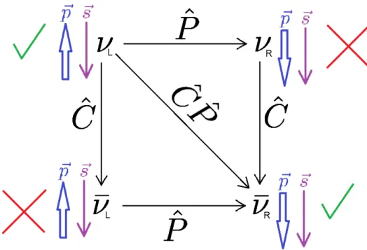
After the discovery of parity violation in weak interactions, it was assumed that the combination of charge and parity must be conserved. Applying them simultaneously is called CP transformation. It transforms a particle into its antiparticle and switches the handedness. This can be seen in Fig. 2.2. If we assume neutrinos to be massless, only left-handed neutrinos and right-handed antineutrinos can be created in weak interactions.
The CP operator transforms a left-handed neutrino into a right-handed antineutrino, which then is allowed again.
Generally a particle that is produced in strong interactions is in a strong flavor eigenstate
|Xi. Applying the CP transformation
CPd|Xi=eiξ X¯
(2.5) transforms it into its CP conjugate
X¯
and introduces a phaseξ which is not observable and therefore can be set to zero without loss of generality. The CP eigenstates of the
2.3 Violation of Symmetries
Figure 2.2: Illustration of a CP transformation on a left-handed neutrino (momentum and spin are antiparallel). Assuming massless neutrinos, only left-handed neutrinos and right-handed antineutrinos are allowed in the Standard Model.
corresponding Hamiltonian are then linear combinations of the flavor eigenstates
|X1i=p|Xi+q X¯
(2.6)
|X2i=p|Xi −q X¯
(2.7) wherepandq are complex numbers and have to fulfil
p
2+ q
2 = 1. Since|X1i and|X2i have a defined mass and lifetime they are usually called mass or lifetime eigenstates [15].
The indices 1/2 are then exchanged by L/H for light/heavy or S/Lfor short/long. The CP eigenstates are given as
|Xeveni= 1
√2(|Xi+ X¯
) (2.8)
|Xoddi= 1
√2(|Xi − X¯
) (2.9)
wherep=q = √1
2.
2.3.2.1 The Cronin and Fitch Experiment
The first to experimentally prove that also CP is violated in weak intereactions were J.
W. Cronin and V. L. Fitch in 1964 [16], for which they were awarded the Nobel Prize in
1980. In their experiment they investigated the neutral kaon system
K0
=|d¯si (2.10)
K0
E
= sd¯
. (2.11)
These are produced in strong interactions and hence are flavor eigenstates. CP eigenstates can then be expressed as linear combinations
|K1i= 1
√2( K0
− K0E
) (2.12)
|K2i= 1
√ 2(
K0 +
K0
E
) (2.13)
where |K1i is CP-even and|K2iCP-odd. Kaons can decay into pions. A two pion state
|ππi is CP-even, while a three pion state |πππi is CP-odd. If CP is conserved in these decays only the following decays would be possible:
K1 → ππ (CP−even) (2.14)
K2 → πππ (CP−odd) (2.15)
Before the discovery of the CP violation, already a short- and a long-lived particle KS
and KL were observed. Therefore, people identified
|KSi=|K1i (τS= 0.9·10−10s) (2.16)
|KLi=|K2i (τL= 0.5·10−7s). (2.17)
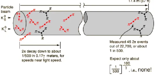
In their experiment Cronin and Fitch created a K0
= √1
2(|K1i+|K2i) beam. This beam then flew through a beam pipe. Due to the shorter lifetime of|K1i all of them should have been decayed at the end of the pipe and only three pion decays should be observed.
2.3 Violation of Symmetries
Figure 2.3: Sketch of the Cronin and Fitch experiment. A particle beam K0
=
√1
2(|K1i+|K2i) is injected into a pipe. Due to the shorter lifetime of|K1ithis contribution should have decayed at the beginning and at the end of the pipe only three pion decays should be observed [17].
The general idea of the experiment can be seen in Fig. 2.3 Out of 22,700 events they observed 45 two pion decays [18]. This was the proof that weak interactions can also violate the CP symmetry. Furthermore, this means that weak or mass eigenstates|KSi and |KLi are not the same as the CP eigenstates as defined in Eq. 2.16 and 2.17. In reality they are superpositions of the CP eigenstates:
|KSi= 1
p1 +||(K1+K2) (2.18)
|KLi= 1
p1 +||(K2+K1) (2.19)
The parameterdetermines the strength of the CP violation and its absolute value has been measured to be≈2.26·10−3 [11]. This means that compared to pure parity, CP is not violated maximally, but only in a small fraction in weak interactions [11, 18, 19].
2.3.3 Types of CP Violation
In the following three types of CP violation are explained:
Violation in Decays
Figure 2.4: CP violation in decays (direct CP violation) [20] (adapted by the author).
CP violation in decays or direct CP violation is described by the following formula:
A¯f¯
Af
6= 1 (2.20)
HereAf and ¯Af¯denote the decay amplitudes for X→f and its CP conjugate ¯X→f¯. In words Eq. 2.20 means that the decay rates of a particleX decaying into a final statef and its antiparticle ¯X decaying into the antiparticle ¯f, are not equal [15].
Violation in Mixing
Figure 2.5:CP violation in mixing (indirect CP violation) [20] (adapted by the author).
CP violation in mixing or indirect CP violation occurs when the rate of a particle oscillating into its antiparticle Γ(X → X) and the rate of the inverse oscillation Γ( ¯¯ X → X) are different. This happens when the absolute values ofp andq in Eq. 2.6 and 2.7 are not equal:
p 6=
q
(2.21)
In words this means that the mass or lifetime eigenstates are not an equal mixture of their flavor eigenstates, which includes that the CP and the mass/lifetime eigenstates do not coincide [11, 15].
2.4 Theoretical Description of the SM and the CKM matrix
Violation in the Interference of Mixing and Decay
Figure 2.6: CP violation in the interference of decays and mixing [20] (adapted by the author).
CP violation in interference between mixing and decay can occur when a particle and its antiparticle can decay to a common final state. Then the two processes X → f and X → X¯ → f can interfere and a phase difference might emerge that causes CP violation. The mathematical condition for this type of CP violation is
Im hA¯f
Af
q p
i
6= 0 (2.22)
which means that the phase does not vanish. This type of CP violation can be observed by measuring the time-dependent asymmetry
A(t) = dΓ[ ¯X→f](t)/dt−dΓ[X→f](t)/dt
dΓ[ ¯X→f](t)/dt+dΓ[X→f](t)/dt (2.23) [15].
2.4 Theoretical Description of the SM and the CKM matrix
At the time of the discovery of CP violation, only the first generation of quarks (up and down) and the strange-quark of the second generation were known. However, there were already experimental hints, like the extremely small branching ratio of flavor changing neutral currents, for the existance of the charm quark. Each quark generation contains one up-type quark with charge 23eand one down-type quark with charge−13e. This quark flavor is conserved in electromagnetic and strong interactions. However, the weak force can change the quark flavor by the exchange of a W± boson. Furthermore, the W boson cannot only change the flavor within one generation, but also between generations. The first to provide a description for this mixing, between the first two generations, was Nicola Cabibbo [21]. He introduced the so called Cabibbo-angle θC. This led to the following
2×2 matrix which transforms the strong or mass eigenstates
d s
into weak eigenstates
d0 s0
[11, 15]. In formulas this looks as follows:
d0 s0
=
cosθC sinθC sinθC cosθC
·
d s
=
Vud Vus Vcd Vcs
·
d s
(2.24)
Since CP violation cannot be explained by a two generation quark theory, Kobayashi and Maskawa extended the Cabibbo matrix, in 1973, to a 3×3 matrix.
VCKM =
Vud Vus Vub Vcd Vcs Vcb
Vtd Vts Vtb
(2.25)
This matrix is known as the Cabibbo-Kobayashi-Maskawa or short CKM matrix. Notably, during the time of their work it was not yet know, that there is a third generation of quarks.
Since the elementsVij of the CKM matrix are complex one initially gets 2·32 = 18 degrees of freedom. Assuming that there are only three generations of quarks, the CKM matrix must be unitary:
V†V =1 (2.26)
For the diagonal elements this gives
3
X
k=1
= Vik
2 != 1 (i= 1,2,3) (2.27)
and for the off-diagonal elements
3
X
k=1
Vik∗Vkj = 0! (i, j = 1,2,3
i6=j). (2.28)
Totally this gives nine equations and therefore this removes nine of the 18 degrees of freedom.
Equation 2.28 describes six equations. Written out three of them for the CKM matrix looks as follows:
VudVus∗ +VcdVcs∗ +VtdVts∗ = 0 (2.29) VudVub∗ +VcdVcb∗+VtdVtb∗ = 0 (2.30) VusVub∗ +VcsVcb∗ +VtsVtb∗ = 0 (2.31)
2.4 Theoretical Description of the SM and the CKM matrix
Figure 2.7: Unitarity triangle representing Eq. 2.30 [15].
These three relations can be represented by triangles, know as unitarity triangles, in the complex plane [15]. For Eq. 2.30 the corresponding triangle can be seen in Fig. 2.7.
The angles α,β and γ are given as α= arg
−VtdVtb∗ VudVub∗
, β = arg
−VcdVcb∗ VtdVtb∗
, γ = arg
−VudVub∗ VcdVcb∗
. (2.32)
Often the triangle is normalized to VcdVcb∗, which shifts the lower side to the real axis in the range [0, 1].
Figure 2.8: Unitarity triangle representing Eq. 2.30 normalized to VcdVcb∗ [15].
This can be seen in Fig. 2.8. The apex (highest point of the triangle) after the normalization has the coordinates
¯
ρ+ i¯η= VudVubV∗
VcdVcb∗ . (2.33)
The unitarity triangles are a nice visualization of consistency checks for the SM. Only if the sides and angles match a closed triangle, the SM is correct. Deviations would indicate new physics beyond the SM [15].
The unitarity condition of the CKM matrix already removed nine of the initially 18 degrees of freedom. Furthermore, five represent phases, which can be absorbed into the quark fields, since an overall phase does not change physics. This then leaves four independent parameters. Kobayashi and Maskawa chose three mixing anglesθ12(Cabibbo angle),θ13,θ23 and a phaseδ. Their parametrization of the CKM matrix takes the form
VCKM =
c12c13 s12c13 s13e−iδ
−s12c23−c12s23s13eiδ c12c23−s12s23s13eiδ s23c13
s12s23−c12s23s13eiδ −c12s23−s12c23s13 c23c13
(2.34)
where sij = sinθij and cij = cosθij. The phase δ is responsible for the CP violation in the quark sector. In a two quark theory this phase factor does not occur and therefore CP violation cannot be explained with only two generations of quarks.
Another representation of the CKM matrix is the Wolfenstein parametrization using the four parametersλ,A,ρand η, which are defined as follows:
λ=s12=
Vus q
Vus
2+ Vud
2 (2.35)
A= s23
λ2 (2.36)
ρ+ iη= s13eiδ
Aλ3 (2.37)
The experimental fact that θ13θ23θ121 can be used to expand the CKM matrix inλ. In the Wolfenstein parametrization expanded up to the third order the CKM matrix then takes this form:
VCKM =
1−12λ2 λ Aλ3(ρ−iη)
−λ 1−12λ2 Aλ2 Aλ3(1−ρ−iη) −Aλ2 1
+O(λ4) (2.38)
The phase factors are approximately zero in all elements, except forVub and Vtd. Hence, for example hadrons containing b quarks are good candidates to search for large CP violating behavior [11, 15].
2.5 The B-factories BaBar and Belle
2.5 The B-factories BaBar and Belle
This theory led to the construction of theBaBar experiment at SLAC in the USA and the Belle experiment at KEK in Japan, dedicated to investigate CP violation in the decay of B mesons. The production of these B mesons is done by asymmetric electron positron colliders (PEP-II for BaBar and KEKB for Belle), operated at the Υ(4S) resonance, which is the third radially excited state of a b¯bquarkonium. It has a mass of 10.58 GeV which is just enough to decay into two B mesons with a mass of 5.28 GeV respectively [7]. These BB¯ pairs are produced in an entangled P-wave and evolve coherently. Therefore, the decay flavor of one of the B mesons determines the flavor of the other one at this point of time.
The difference of the decay times ∆t=t1−t2between the two B mesons is used to observe time-dependant CP violation. The asymmetry of the collider boosts the B mesons into the forward direction and the time difference is translated into a spatial distance, which is measured. The flavor of the second B meson together with the time difference between
Figure 2.9: Principle of time-dependant CP violation measurements in B factories. The asymmetric beam energies boost the B mesons into the forward direction and the time difference of the decays is translated into a spatial distance [22].
the decays provide a method to measure the time dependant CP asymmetry [6, 20, 23].
The principle of these measurements can be seen in Fig. 2.9.
BaBar and Belle were able to confirm the theory of Kobayashi and Maskawa up toO(10%) and they were awarded the Nobel Prize in 2008.
Figure 2.10 shows the global fit of the unitarity triangle in the ¯ρ-¯η plane from 2018, including several constrains, like the light green band given by measurements of KK¯ mixing or the yellow and orange bands given by BB¯ andBsB¯s mixing [25].
However, there are still inconsistencies in some measurements and the measured ratio of CP violation is many magnitudes to small to explain the observed baryon asymmetry.
Hence, particle physicists search for new physics with significant deviations from the SM.
Figure 2.10: Global fit of the unitarity triangle (representing Eq. 2.30) in the ¯ρ-¯η plane [24].
For these measurements BaBar and Belle are not precise enough. Therefore, the KEKB accelerator and the Belle detector were upgraded to the SuperKEKB accelerator and the Belle II detector in the past years.
3 SuperKEKB and Belle II
3.1 The SuperKEKB Accelerator
The main upgrade of SuperKEKB is the increase of luminosity1, which means more data, more statistics, which decreases the statistical uncertainties and in the end means more precise measurements. Compared to its predecessor KEKB, the luminosity is increased by a factor of 40, yielding an unprecedented peak luminosity of 8×1035cm−2s−1 [26]. The luminosity can be calculated with
L= γ±
2ere
1 + σy∗
σ∗x
I±ξy±
βy∗
RL Rξy
(3.1) whereγ± are the Lorentz factors of the bunches,reandethe classical electron radius and charge, σx,y∗ the beam sizes at the interaction point (IP). RL andRξy denote correction factors needed due to the hourglass effect and the crossing angle at the IP (for details see [5]). I± are the beam currents, ξy± the vertical beam-beam tune-shift parameters and βy∗ are the vertical beta functions at the IP. Assuming a Gaussian beam profile with widthσ, the beta function is given as
β= σ2
(3.2)
whereis the emittance of a particle beam [27].
To increase the peak luminosity by a factor of 40 the beam currents are doubled and the vertical beta function βy∗ is reduced to 1/20 compared to KEKB [5]. This is achieved with focusing magnets (QCS), which decrease the beam sizes (σ∗x,y) at the IP. With this SuperKEKB aims to collect 50 ab−1 of data until 2027 (see Fig. 3.1).
To detect this enormous amount of data, also the detector is upgraded. Belle II has a newly designed data-aqusition system, as well as reworked subdetectors. Furthermore, a pixel detector (PXD) is added, to improve the resolution of particle tracking, which is needed for time-dependant studies of CP violation [28].
3.2 The Belle II Detector
The Belle II detector is a so called 4π-detector, meaning it is arranged cylindrically around the beam pipe and closed by endcaps, therefore covering almost the entire solid angle, with
1The luminosity describes the amount of collisions per area and time and is therefore a quantity that describes the amount of data produced by an accelerator
Figure 3.1: Projected luminosity of the SuperKEKB accelerator [26].
the IP in the center. It consists of several sub-detectors, each of them measuring a specific property, which are arranged in an onion-like shell-on-shell structure. The combination of all the informations of each sub-detector makes it possible to study the particles and their properties, created by the colliding particles.
3.3 Vertex Detector VXD
The innermost detector is the VXD, which itself consists of two sub-detectors. The Pixel Vertex Detector PXD, which is placed around the beam-pipe and the Silicon Vertex Detector SVD, covering the PXD. The PXD consists of two layers of DEPFET (DEpleted P-channel Field Effect Transistor) pixels. It is supposed to detect passing particles very precisely to reconstruct the origin or vertex of these particles (The PXD is explained more thoroughly in chapter 4).
The SVD are four layers of double-sided silicon stripdetectors, with its innermost layer having a radius of 38 mm and its outermost layer having a radius of 140 mm. The SVD has an angular acceptance of 17◦ < θ <150◦. The task of the SVD is to reconstruct tracks, created by particles passing it. Central Drift Chamber (CDC) tracks can be extrapolated with information from the SVD, which then allows, together with the PXD, to reconstruct the vertex. This also requires a low occupancy to make sure SVD hits are associated to
3.4 Central Drift Chamber CDC
Figure 3.2: Sketch of the Belle II detector with all its sub-detectors [29].
the correct CDC track. Furthermore, the SVD can reconstruct low momentum tracks that do not reach the CDC [22] [30].
3.4 Central Drift Chamber CDC
The next sub-detector is the Central Drift Chamber. The CDC is a cylindrical wire chamber filled with a gas (He−C2H6) and contains 14 336 sense wires, arranged in 56 cylindrical layers, which are held at a high voltage. Particles passing the CDC ionize the gas and create electrons which are then drift towards the sense wires where they create an avalanche of secondary electrons in the strong electric field close to the wire, which then yield a measurable signal. The CDC has several important tasks. First, it is able to reconstruct charged tracks and measure their momenta. Second, it can be used for particle identification of low momentum particles by measuring the energy loss within the gas. Additionally it provides trigger signals to reduce the amount of data by throwing away events which do not originate from the IP and therefore constiute uninteresting background [30].
Figure 3.3:Sketch of the Vertex Detector, containing the two layered PXD in the inside, which is coverd by four layers of the SVD [22].
3.5 Time-Of-Propagation TOP counters
The TOP counters are used for precise timing and also for particle identification in the central region of the detector. TOP counter modules consist of quartz bars in which Cherenkov light is created by charged particles traversing the bars. This light travels through the bar (total internal reflection) until it reaches micro-channel photomultiplier tubes (MCPMTs), highly segmented in the x and y directions, at one end of the bar.
The timing information from the MCPMTs together with the x-y coordinates makes it possible to reconstruct the Cherenkov image (see Fig. 3.4). One of the main tasks of the TOP counters is the differentiation of kaons and pions by determining the different angle of the Cherenkov cone in the quartz bars (see Fig. 3.5) [30, 31].
3.6 Aerogel Ring-Imaging Cherenkov ARICH detector
Particle identification in the forward endcap region is done by the ARICH counters.
They consist of aerogel tiles as radiators, position sensitive photon detectors and readout electronics. Just like in TOP, particles passing the aerogel tiles, create Cherenkov light.
The photon detectors are sensitive to single photons and are highly tolerant of the high radiation environment. In total ARICH contains 124 pairs of aerogel tiles, 420 Hybrid Avalanche Photo-Detectors and covers an area of 3.5 m2. The task of the ARICH counters
3.7 Electromagnetic Calorimeter ECL
Figure 3.4: Illustration of one TOP counter [31].
Figure 3.5: Working principle of a TOP counter to distinguish kaons and pions [31].
is to separate kaons and pions as well as the discrimination of pions, muons and electrons below 1 GeV [30, 31].
3.7 Electromagnetic Calorimeter ECL
The detector that covers TOP is the ECL, which is supposed to measure the energy of passing photons. It determines their energies and angular coordinates. Furthermore, it identifies electrons and provides trigger signals. The ECL has an inner barrel section and two endcaps. In total it consists of 8736 crystals, 6624 CsI(Tl) crystals in the barrel region and 2112 CsI crystals in the two endcap regions. Scintillation light is created inside these crystals, by electrons and positrons in an electromagnetic shower created from incoming photons and electrons (positrons). This light is then detected by photodiodes [30].
3.8 Solenoid Magnet
The inner parts of the Belle II detector, including the ECL, are covered by a supercon- ducting solenoid with a length of 4.4 m and a diameter of 3.4 m. The solenoid is able to create a magnetic field of 1.5 T, which bends the tracks of charged particles and makes it possible e.g. for the CDC to determine their momenta [30].
3.9 K
Land µ detector KLM
The outermost detector of Belle II is the KLM. It is also separated into a barrel and two endcap regions. The KLM consists of alternating 4.7 cm thick iron plates and active detector elements.
Muons with high enough energies traverse the KLM on an almost straight line. KL
mesons create hadronic showers which are detected in the ECL, the KLM or both. To detect charged particles the KLM in the Belle detector used glass-electrode resistive plate chambers (RPCs). Two of these glass electrodes are separated by a 1.9 mm thick gap which is filled with a gas mixture. They are held at a high voltage, which provides an electric field of 4.3 kV mm−1. Charged particles ionize the gas and due to the electric field, a current is initiated, which is measured by readout strips on the RCPs. However, the efficiency of the RPCs significantly decreases with higher backgrounds as expected in Belle II. Therefore, the RPCs in the two innermost layers and in the endcaps were replaced by scintillator strips with wavelength shifting fibres wich can stand higher rates. Silicon photomultiplier tubes (SiPMs) are used to read out the wavelength-shifted scintillation light [30, 32].
4 Pixel Vertex Detector
The predecessor of Belle II (i.e. Belle) contained a VXD consisting only of a strip vertex detector. The SuperKEKB accelerator aims for a 40 times larger peak luminosity than KEKB. For a double-sided strip detector this would lead to ambiguities at high rates, due to the high occupancy. Therefore, the inner two layers of the VXD are replaced with a newly developed pixel detector, the PXD, which is based on DEPFET (DEpleted P-channel Field Effect Transistor) pixels. It must have a fast readout mechanism in order to reduce the occupancy. Furthermore, the PXD needs to have a large radiation hardness, in particular to withstand the increased radiation caused by background. In addition, the PXD must have a high spatial resolution to execute its main task, the reconstruction of vertices. Therefore, it should be very thin, since thicker detectors gives rise to multiple scattering which negatively influences the spatial resolution [22].
The new PXD consists of two layers of self-supporting ladders, which are arranged in a windmill structure around the beam pipe at radii of 14 mm and 22 mm. An illustration of
Figure 4.1: Layout of the Pixel Vertex Detector. It consists of two layers of ladders, eight in the inner layer and twelve in the outer layer [33].
the PXD can be seen in Fig. 4.1. Each ladder are two glued-together modules. Therefore, there are four different module types. Inner-foward and inner-backward (IF and IB)
for layer 1 and outer-foward and outer-backward (OF and OB) for layer 2. Due to problems during this gluing (see chapter 7), currently only the inner layer of the PXD is complete, while the outer layer only contains two ladders. This is sufficient for the current luminosities of the SuperKEKB accelerator since all the resolution is given with the inner layer. The outer layer is mainly needed for background suppression, which will be important for the high luminosity runs in the future. Hence, the PXD of course needs to be completed.
Each module contains 768rows×250columns= 192000 DEPFET pixels. A module is controlled by three different ASICs (Application Specific Integrated Circuits), six Switchers, four DHPs (Data Handling Processors) and four DCDs (Drain Current Digitizers).
4.1 DEPFET
The pixels of the PXD are based on so called DEpleted P-channel Field Effect Transistor (DEPFET) technology, where a cross-section of a single pixel can be seen in Fig. 4.2. The idea is that a p-channel Metal-Oxide-Semiconductor Field-Effect Transistor (MOSFET) is placed on top of a n-type sideward fully-depleted silicon bulk. Particles passing this bulk create electron-hole pairs. The holes drift to ap+ implant at the bottom of the pixel. The electrons are used as signal. To accumulate them, there is an additional n-doped region under the MOSFET gate, called internal gate. Electrons in the internal gate influence the Source-Drain current of the MOSFET due to capacitive coupling. The modulated Source-Drain current is then the signal. One advantage of the DEPFET technology is that
Figure 4.2:Profile of a DEPFET pixel in the x-y plane (left) and in the y-z plane (right).
Particles passing the depleted region create electron-hole pairs. The electrons accumulate in the internal gate, where they influence the Source-Drain current of the MOSFET. To reset the pixel it contains an+ doped region (ClearGate), where a high positive voltage can be applied to remove the electrons of the internal gate [22].
4.2 ASICs
the electrons are stored in the internal gate and the pixel can be read out multiple times without destroying the signal. There is an additionaln+ doped region, where a positive voltage can be applied to remove the electrons of the internal gate. Moreover, there is a p-well below the clear region (see right side of Fig. 4.2) to prevent back-injection, i.e.
electrons drifting from the clear region into the internal gate [22, 34, 35].
4.2 ASICs
A PXD module consists of a sensitive area of DEPFET pixels and three different ASICs to provide the voltages, clocks and to handle the readout. The ASICs, the DEPFET
Figure 4.3: Sketch of the ASICs on a PXD module and their interplay [22].
matrix, their internal connections and the readout connections can be seen in Fig. 4.3.
4.2.1 Switcher
The first of these ASICs is called Switcher. A Switcher controls the gate and clear voltages of the DEPFET pixels. One Switcher has 32 channels. Totally, six Switchers are mounted on one PXD module, with 192 electrical rows1.
4.2.2 DCD
The Drain Current Digitizer (DCD) digitizes the Drain currents of the DEPFET pixels.
For this purpose the DCD has 256 input channels of which 250 are connected to Drain lines of the matrix. One PXD module contains four DCDs, which are connected to the 1000 Drain lines2. The digitization is done with a resolution of 8 bit and takes about 100 ns. The dynamic range of the ADCs is approximately 20µA. The digitized signal is then sent to the last ASIC, the DHP [22, 35, 36, 37].
4.2.3 DHP
Four Data Handling Processor (DHP) ASICs receive the digitized 8 bit signal from the four DCDs. The main task of the DHP is the procession and reduction of data. First of all it performs a zero-suppression. This means that only the data of pixels, which have a value higher than a certain threshold are sent out. Furthermore, it is able to remove common mode noise3. Moreover, the Switchers and the DCDs are controlled by the DHPs.
Via a 1.6 Gbps high-speed link the processed data is then transfered off the module to the data acquisition system [22, 35].
4.3 PXD Modules and their Readout
The layout of a complete PXD module can be seen in Fig. 4.4. The main part is the sensitive area or matrix consisting out of 192000 DEPFET pixels. This area is thinned to 75µm. Closer to the IP the pixels are smaller and further away they are larger (see Tab. 4.1). The reason for this design is that closer to the IP particles cross the detector on a rather perpendicular track, which means less charge sharing4 between pixels and therefore lower resolution. To cope with this the pixels are made smaller here. Further away from the IP the particles cross the detector with a narrow angle which yields more charge sharing and better resolution. Hence, larger pixels are sufficient. Furthermore, this
1An electrical row is the combination of four consecutive pixel rows: 768pixel rows4 = 192electrical rows.
2Since one electrical row contains four pixel rows, four Drain lines per pixel column are needed.
3Common mode noise, describes random oscillations in electrical lines, caused by coupling them to external conductors (e.g. chassis, grounding, ...) or by picking up electromagnetic radiation.
4Charge sharing describes the effect when particles leave a signal in multiple neighbouring pixels.
Therefore, the total signal is distributed over multiple pixels and a better resolution of the direction of the incoming particle can be achieved, compared to the case when only one pixel is crossed.
4.4 Off-Module Electronics
is a compromise between high positional resolution and fast readout. In total each matrix consists of 256×250 small pixels and 512×250 large pixels.
The sensitive area is surrounded by 525µm rims giving the modules a self-supporting hardness. The Switchers are mounted on the balcony and the DCDs and the DHPs on the end-of-stave5. Since the PXD contains two layers and has a forward and a backward direction there are four different module designs (IF, OF, IB, OB). The outer modules are slightly larger then the inner modules. The dimensions of the modules can be read off
length width small pixel large pixel Layer 1 67.975 mm 15.4 mm 55 × 50 mm
260 × 50 mm
2Layer 2 84.975 mm 15.4 mm 70 × 50 mm
285 × 50 mm
2Table 4.1:Dimensions of the PXD modules and their pixel sizes. Closer to the IP the pixels are smaller and further away they are larger (see Fig. 4.4) [22].
in Tab. 4.1. Furthermore, forward and backward modules differ on the side where the Switchers are mounted (right or left).
Electrically one Gate and Clear line controls four consecutive geometrical pixel rows.
Hence, four Drain lines per pixel column are needed to read out every individual pixel.
Totally, one module contains 192 Gate and Clear lines and 1000 Drain lines. The readout is performed in the so called rolling shutter mode. This means that the module is readout Gate after Gate, where one Gate activates four geometrical DEPFET pixel rows. Hence, 1000 pixels are read out simultaneously. The readout of a single pixel lasts approximately 100 ns (at the same time 999 other pixels are read out). Therefore, the readout of an entire module lasts approximately 20µs [22, 35].
4.4 Off-Module Electronics
At the end-of-stave aKapton cable is soldered to the module. This cable is connected to a PatchPanel which separates the power lines, the high-speed lines for the data transfer and the slow-control lines. The off-module readout and control system is called Data Handling Hub (DHH). It contains one Data Handling Engine (DHE) per module, which receives the data sent out by the DHP ASICs. The Data Handling Concentrater groups together five DHEs. Afterwards, the data is sent to the ONSEN (Online Selection Node) system. By the determination of regions of interest, together with informations from other subdetectors (mainly the SVD and CDC), ONSEN reduces the acquired data by a factor of 30. From ONSEN the reduced data is sent to the global Belle II DAQ [35, 38, 39].
5The end-of-stave is the end of the module, which is away from the IP.
Figure 4.4: Layout of a PXD module. (a) One module consists of 192000 pixels, smaller pixels closer to the IP and larger pixels further away. The six Switchers are mounted on the balcony and the DCDs and DHPs on the end-of-stave of the module. (b) Electrical connections on the modules. One Clear and Gate line controls four geometrical pixel rows.
Therefore, every pixel column needs four Drain lines four the readout mechanism [22]
(adapted by the author).
Additionally, the DHH contains a Data Handling Isolator (DHI), which programs the module ASICs, via slow control, and distributes clock and trigger signals [40].
4.4 Off-Module Electronics
Figure 4.5: Sketch of the readout via the rolling shutter mode. The module is read out Gate after Gate. In the sketch the orange row represents the currently active Gate row and the green arrows depict the Drain currents flowing into the DCDs [22].
5 Tests and Characterization of PXD Modules
Every module that is produced has to undergo several tests to evaluate its functionality and characterize it. All these test are written down in a handbook to assure every module undergoes the same mass-testing procedure independent of the setup location (the work- load has been split between several sites of the collaboration). It starts with the mechanical mounting of the module in the setup and explains the required software preparations.
Subsequently follows the first power-up. Afterwards following tests/measurements are performed:
High Speed Link Scan
The first measurement is a high speed link scan, which aims to optimize the link quality between the DHP and the DHE. It scans over three parameters, adjusting the amplitude, the pre-emphasis and the length of the pre-emphasis. For each con- figuration the link is evaluated by the corresponding eye value, which indicates the strength of a digital signal/link [22]. Afterwards, the best combination is determined and adjusted.
Delay Scan
To assure proper data transmission between the ASICs (from DCD to DHP) a delay scan is performed. For this purpose a predefined test pattern is enabled in the DCD which is constantly sent to the DHP. It scans through two delay variables and compares the pattern that the DHP reads with the original test pattern of the DCD.
For each configuration the amount of bit errors are evaluated and the best settings are uploaded.
Pedestals
After the transmission lines are adjusted correctly a module can be read out. A pedestal value of a DEPFET pixel is the Source-Drain current of the enabled MOS- FET without an external signal. This means there are no electrons accumulated in the internal gate and the Drain current is just modulated by the voltage applied at the external gate. The pedestal map for one module (W45 OF11), where 100 frames were averaged, can be seen on the right side of Fig. 5.1. The map is separated into
1W45 OF1: first outer-foward (OF) module of wafer 45.
Figure 5.1: Pedestal values for 100 frames for module W45 OF1. Right: Pedestal map separated for the four asicpairs (APs), Left: Pedestal distribution.
four regions corresponding to the four asicpairs2 (APs). AP1 has a broken Drain line at row 559 and column 192. Therefore, only about one-third of this column can be readout. The left side of the figure shows the distribution of the pedestal values (for 100 frames) in different colours for each AP and stacked on each other. In the experiment the pedestals are subtracted from the measured Source-Drain currents (zero-suppression). A signal is defined as a Source-Drain current that is above a
certain threshold after the zero-suppression.
Temperatures
The next step in the mass-testing procedure are temperature measurements of the DHPs at different operation states of the module (e.g. only ASICs powered or complete module, including DEPFET matrix powered). The temperatures should not exceed a certain value, i.e. 85◦C, since the module could be damaged. In the lab setups the modules are cooled with water while the experiment at KEK uses a liquid CO2 cooling system.
2An asicpair is the combination of one DCD and the corresponding DHP.
ADC Curves
Afterwards, several ADC transfer curves for the channels of the DCD are recorded.
This is done by swiping the gate voltages of the MOSFETs of the module and therefore swiping the Drain currents of the DEPFET pixels for different internal settings of the DCDs. The analysis determines the best combination in order to achieve a linear ADC behavior (for details see [22]).
Offset Calibration
One important step in the characterization is the Offset Calibration, which aims to narrow down the pedestal spread to match the dynamic range of the DCDs. These differences between pixels mainly originate in the production of the modules, e.g.
due to inhomogeneous doping [22]. To shrink the spread, a current
IOf f set = (0, 1, 2, 3) ·IDAQ−glo (5.1) can be added individually to each pixel. This current is composed of a global current IDAQ−gloand a pixel-individual multiplication factor. Therefore, the Offset Calibra- tion should in theory be able to suppress the pedestal spread by a factor of four.
The Offset Calibration performs a 2D scan throughIDAQ−gloand the multiplication factor and takes pedestals for each combination. Afterwards an analysis algorithm determines the optimal settings (for details see [41]). An example of the impact of
(a)Without Offsets (b)With Offsets
Figure 5.2: Comparison between the pedestals of module W03 OF2 without and with Offset Compensation.
the Offset Compensation on the pedestals of one module (W03 OF2) can be seen in Fig. 5.2.
Source Scan
The last step in the mass-testing procedure is a source scan with a radioactive source.
The source (at MPP a109Cd source is used) is driven over the matrix while different DEPFET voltages (HighVoltage3, Drift4 and ClearOff5) are scanned. Afterwards the optimal configurations are adjusted and the amount of not working pixels is determined. A module with more than approximately 1% dead pixels is graded
‘Class B’, while modules with more than 99% working pixels are graded ‘Class A’.
3The HighVoltage depletes the silicon bulk of the DEPFET pixels by removing all charge carrier.
4The Drift potential prevents the back injection from the clear region into the internal gate.
5ClearOff switches the MOSFET off by applying a voltage in reverse direction.
6 Pre-Offset VNSubIn Adjustment
6.1 Motivation
The Offsets of modules need to be recalibrated from time to time at KEK, due to radiation damages caused by inhomogeneous irradiation. As a starting point of the Offset Calibration the pedestals need to be in the lower region of the dynamic range, since the offsets add a current to the pixels and therefore shift the pedestals to higher ADU values.
To shift the pedestals to lower ADU values there are several currents that can be added or subtracted from the Drain currents within the DCDs. IPAddIn and VNSubIn are added/subtracted before the trans-impedance amplifier of the DCD, while IPAddOut and VNSubOut are added/subtracted afterwards (for details see [37]). To shift the pedestals to lower regions often VNSubIn is adjusted. Higher VNSubIn values subtract higher currents from the Drain current before the trans-impedance amplifier and therefore shift the pedestals further to lower values.
The procedure for a shifter is to take pedestals, adjust the VNSubIn values and take pedestals again to see how the pedestals changed. This is repeated until the pedestals start at the lower edge of the dynamic range. To prepare the whole PXD for the Offset Calibration this needs to be done for 40 modules manually, which is quite time-consuming.
During data taking of the Belle II detector the sub detectors only have two times 20 minutes a week for local calibrations. Therefore, an automatized method is needed, which quickly shifts all pedestals of all modules in the desired position before the Offset Calibration. For this purpose a script has been developed, which will be explained in the following.
6.2 Method
The basic idea of this script is to mimic a shifter. This means to take pedestals, analyse them and then calculate new VNSubIn values. Afterwards take pedestals and analyse them again. This procedure is repeated until the pedestals are in the desired region, which will be explained in this section. The termination criterion is that the new and the old VNSubIn values between two iterations maximally differ by one. The analysis of the pedestals is based on their median1. The median is chosen, because compared to e.g. the
1The value of each pixel is recorded 100 times and averaged. Afterwards the median of all pixels is determined.
mean it is less dependent on excesses in the distribution. The mean would be shifted by very hot2 ordead3 pixels, while the median is not.
The aim is to shift the pedestals to a wanted median. The calculation of the VNSubIn values for the next iteration is based on the following formula:
V N SubInnew=V N SubIncur+w· (M ediancur−M edianwanted) (6.1) Here V N SubIncur are the current VNSubIn values, M ediancur and M edianwanted are the current and the wanted median and w is a factor <1 needed, since already small changes in VNSubIn have a large impact on the position of the pedestals. Tests with modules in the MPP lab setups have shown thatw= 0.04 andM edianwanted= 50 work well. Rewriting Eq. 6.1 yields:
V N SubInnew−V N SubIncur=V N SubIndif f =w· (M ediancur−M edianwanted) (6.2) A plot of V N SubIndif f depending onM ediancur is depicted in Fig. 6.1. Basically it is just a linear step function with slopew= 0.04. The step-shape appears since VNSubIn can only take integer values. The first feature that can be seen is, that for small current
0 50 100 150 200 250
Median
curin [ADU]
2 0 2 4 6 8 10
VN Su bIn
diff12.5 87.5
w * (Median
curMedian
wanted)
w = 0.04, Median
wanted= 50ADU
Figure 6.1: Difference between the new and current VNSubIn values depending on the current median forw= 0.4.
2Hot pixels are pixels that always show a high Drain current, although they are not switched on.
3Dead pixels are pixels that do not show any signal at all, i.e. their Drain current is below the dynamic ADC range.
6.2 Method
medians, the VNSubIn values are maximally shifted by two, which might be too small and therefore takes too many iterations. To cope this, the script shifts the values of VNSubIn per default by 5, if the median lies within the edge bins (0 or 1).
On the other end of the dynamic range the VNSubIn values are shifted by 8, if the median lies in a bin higher than 237 ADU. A shift of eight is already pretty large, but still considered reasonable.
The reddish area shows the accepted range, meaning the range where the values of VNSubIn between two iterations are maximally shifted by one, around the wanted median, and therefore considered as well enough optimized. Forw= 0.04 and a wanted median of 50 ADU the boundaries range from 12.5 ADU to 87.5 ADU which is quite big. On can decrease this area by increasing the w-factor and therefore decreasing the step-size of the function. On the other hand this would also lead to bigger changes in V N SubIndif f and the script might overshoot the accepted range. The behavior of this function for two other
0 50 100 150 200 250
Mediancur in [ADU]
2 0 2 4 6 8 10
VNSubIndiff
20.0 80.0
w * (Mediancur Medianwanted)
w = 0.05, Medianwanted= 50ADU
(a)w= 0.05
0 50 100 150 200 250
Mediancur in [ADU]
2 0 2 4 6 8 10
VNSubIndiff
0.0 100.0
w * (Mediancur Medianwanted)
w = 0.03, Medianwanted= 50ADU
(b) w= 0.03
Figure 6.2:Comparison of the function to calculateV N SubIndif f for differentw-factors.
w-factors can be seen in Fig. 6.2. Forw= 0.05 the accepted area is between 20 ADU to 80 ADU, but for high current medians the values of VNSubIn are changed by ten. For w= 0.03 the accepted area then already goes from 0 to 100, which is way too large.
As mentioned above for the performed tests, w= 0.04 worked well, but if needed it can be easily further fine-tuned.
6.2.1 Additional Features
The script contains two additional features, which will be addressed in this section. First, theanalog common mode correction (ACMC) is turned off during the scan. The ACMC is an internal feature of the DCDs to compensate common mode noise [22]. It would also compensate the effect of the VNSubIn shifts, since it calculates the mean of all connected pixels and subtracts this value from each pixel individually. Therefore, it needs to be turned off.
Secondly, the script uses a pedestal mask (an example can be seen in Fig. 6.3), which is
![Figure 2.8: Unitarity triangle representing Eq. 2.30 normalized to V cd V cb ∗ [15].](https://thumb-eu.123doks.com/thumbv2/1library_info/3998843.1540309/21.892.205.657.657.917/figure-unitarity-triangle-representing-eq-normalized-v-cd.webp)
![Figure 2.9: Principle of time-dependant CP violation measurements in B factories. The asymmetric beam energies boost the B mesons into the forward direction and the time difference of the decays is translated into a spatial distance [22].](https://thumb-eu.123doks.com/thumbv2/1library_info/3998843.1540309/23.892.124.711.490.707/principle-dependant-violation-measurements-factories-asymmetric-difference-translated.webp)
![Figure 2.10: Global fit of the unitarity triangle (representing Eq. 2.30) in the ¯ ρ-¯ η plane [24].](https://thumb-eu.123doks.com/thumbv2/1library_info/3998843.1540309/24.892.177.763.223.781/figure-global-fit-unitarity-triangle-representing-eq-plane.webp)
![Figure 3.1: Projected luminosity of the SuperKEKB accelerator [26].](https://thumb-eu.123doks.com/thumbv2/1library_info/3998843.1540309/26.892.174.781.186.521/figure-projected-luminosity-superkekb-accelerator.webp)
![Figure 3.2: Sketch of the Belle II detector with all its sub-detectors [29].](https://thumb-eu.123doks.com/thumbv2/1library_info/3998843.1540309/27.892.105.735.183.582/figure-sketch-belle-ii-detector-sub-detectors.webp)
![Figure 3.3: Sketch of the Vertex Detector, containing the two layered PXD in the inside, which is coverd by four layers of the SVD [22].](https://thumb-eu.123doks.com/thumbv2/1library_info/3998843.1540309/28.892.203.745.168.532/figure-sketch-vertex-detector-containing-layered-inside-coverd.webp)
