Ludwig-Maximilians-University Munich
Faculty of Physics
Master Thesis
Testing of the Gated Mode for the Belle II Pixel Detector
Submitted by: Dr. Eduard Prinker
Referee: Prof. Dr. Christian Kiesling
Munich, August 2015
Abstract
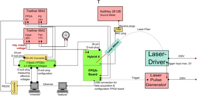
DEPFET pixel sensors offer intrinsic amplification, low mass and a very high signal to noise ratio. They form an integral building block for the vertex detector system of the Belle II experiment, which will start data taking in the year 2017 at the new Super- KEKB electron-positron collider in Japan. The particle bunch currents have a rather short lifetime in the order of 10 minutes. To keep the significantly increased luminosity of the collider constant over time, the bunch currents have to be topped off by injecting daughter bunches at a rate of 50 Hz. The particles in the daughter bunches produce a high rate of background (“noisy bunches”) for a short period of time, saturating the oc- cupancy of the sensor. Operating the DEPFET sensor in a so far unexplored new mode (“Gated Mode”) allows preserving the signals from collisions of normal bunches while protecting the pixels from background signals of the passing noisy bunches. A special test board (Hybrid 4.1) is used, which contains a small version of the DEPFET sensor with a read-out (DCDB) and a steering chip (SwitcherB) attached, both con- trolled by a field-programmable gate array (FPGA) as the central interface to the com- puter. Experimental results presented in this thesis demonstrate that the Gated Mode can be efficiently operated at full target operation speed of 320 MHz.
Zusammenfassung
DEPFET Pixelsensoren zeichnen sich insbesondere durch ihre geringe Masse und ein hohes Signal/Rausch-Verhältnis aus. Sie bilden einen integralen Bestandteil des Belle II Vertex-Detektor-Systems am SuperKEKB Elektron-Positron-Beschleuniger in Japan, dessen Fertigstellung für 2017 geplant ist. Um die vorhandene, stark gestiegene Lumi- nosität des Beschleunigers aufrechtzuerhalten, müssen die Teilchenpakete, deren durchschnittliche Lebensdauer ungefähr 10 Minuten beträgt, regelmäßig erneuert wer- den. Konkret werden alle 20 Millisekunden zwei zusätzliche Teilchenpakete in den Be- schleuniger eingespeist. Die neu injizierten Teilchen verursachen zwischenzeitlich ein hohes Hintergrundrauschen. Dadurch stellen sich die Detektoraufzeichnungen als stark verzerrt und somit unbrauchbar dar. Eine spezielle Betriebsweise des DEPFET Sen- sors, der sogenannte „Gated Mode“ ermöglicht es, dass bereits aufgezeichnete Signa- le erhalten bleiben und keine kontaminierte Ladung die Detektoreffizienz beeinträchtigt.
Der Testaufbau umfasst eine spezielle Leiterplatte (Hybrid 4.1). Darauf sind alle we- sentlichen Elemente des Belle II Pixeldetektors wie DEPFET Sensor, Auslesechip (DCDB) und Steuerungschip (SwitcherB) installiert. Ein zwischengeschalteter Field Programmable Gate Array (FPGA) – ein programmierbarer Schaltkreis der Digital- technik – dient als Verbindung zum Computer. Experimentelle Ergebnisse dieser Mas- terarbeit lassen darauf schließen, dass der Gated-Mode-Betrieb auch bei der geplan- ten Zielfrequenz von 320 MHz ausgezeichnet funktioniert.
Contents
Abstract ... 2
Contents ... 3
1 Introduction ... 6
2 Physics at Belle II ... 7
2.1 Basic Motivation: benefit of a Super Flavor Factory (SFF) ... 7
2.2 BELLE II Detector System ... 12
2.3 SuperKEKB injection scheme ... 14
2.3.1 Principles of particle acceleration ... 14
2.3.2 Beam Parameters increasing Luminosity ... 14
2.3.3 Nano beam scheme ... 16
2.3.4 Beam life time and dead-time during injection ... 18
3 DEPFET Sensors ... 22
3.1 DEPFET Operation... 23
3.1.1 The DEPFET Principle ... 23
3.1.2 Electrical properties of DEPFET devices ... 25
3.1.3 Readout of DEPFET Pixel Matrices ... 27
3.1.4 Clear Process ... 29
3.1.5 Parasitic Capacitances of a DEPFET Matrix... 30
3.2 DEPFET Technology & Design... 30
3.3 Biasing scheme ... 31
3.4 The Gated Mode ... 34
3.5 PXD Detector ... 35
3.6 PXD Sensor Electronics ... 37
3.6.1 The DCDB pipeline... 38
3.6.2 Switcher-B ... 42
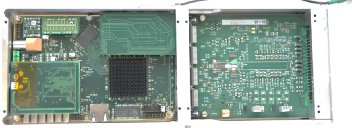
4 Hybrid 4.1 Board and FPGA Board ... 45
4.1 Overview ... 45
4.2 Hybrid 4.1 Board ... 46
4.3 FPGA Board ... 47
5 Test Plan for the Gated Mode ... 49
5.1 Overview ... 49
5.2 Testing of Hybrid4 PCB components ... 50
5.2.1 PXD6-Matrix ... 50
5.2.2 DCDB pipeline Characterization ... 50
5.2.3 SwitcherB Characterization ... 50
5.3 The Gated Mode Analysis ... 51
6 DCDB pipeline Characterization ... 52
6.1 DCDB Test Software ... 52
6.2 Digital functionality check ... 52
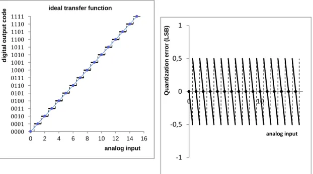
6.3 Conversion Algorithm ... 53
6.4 ADC Error Sources ... 57
6.5 ADC characterization ... 60
6.5.1 Optimize Settings ... 60
6.5.2 Analyzing the ADC Transfer Curves ... 63
7 The Gated Mode Operation ... 69
7.1 Conceptual Approach for testing of the Gated Mode ... 69
7.2 Processing Chain ... 70
7.2.1 DEPFET Readout System ... 70
7.2.2 The Gated Mode Analysis Tool ... 70
7.3 Programming Switcher Sequences ... 74
7.3.1 SwitcherB Strobe Logic ... 74
7.3.2 SwitcherB Controller ... 79
7.4 Calibration Measurement... 80
7.4.1 Interaction of Photons with Silicon ... 80
7.4.2 Laser Intensity Measurements ... 81
7.4.3 Radioactive Source Measurements ... 82
7.5 The Gated Mode Sequences ... 86
7.5.1 Mapping ... 86
7.5.2 Oscilloscope Measurements and Simulation of Strobe Logic ... 86
7.5.3 Experiment A: Signal Charge Preservation ... 89
7.5.4 Experiment B: Junk Charge Prevention ... 93
7.5.5 Pedestal Analysis ... 94
8 Results ... 99
9 Conclusion and Outlook ... 101
Appendix A: B-Meson Decay ... 103
Appendix B: Pair creation of a 660nm Laser in Silicon ... 106
Appendix C: Radioactive Source Formulas ... 109
Appendix D: Optimized Test Setup Voltages ... 111
Appendix E: SwitcherB Sequence Simulation ... 112
Glossary ... 115
List of Figures ... 121
List of Tables ... 124
Acronyms ... 125
Bibliography ... 128
Acknowledgement ... 136
Declaration of originality ... 137
1 Introduction
Citius, altius, fortius, this principle not only governs the Olympic spirit but can also serve as a guideline for particle colliders. In spring 2015 after a two years break the LHC was upgraded to almost its full specified center of mass energy at 14 TeV. The electron positron community on the precision frontier will answer in 2017 with an up- grade of the KEKB collider (“Super-KEKB”) at the KEK laboratory in Tsukuba (Japan).1 This collider will deliver an unprecedented luminosity of almost 1036/cm2 and feature highly innovative technologies. Besides the revolutionary nano beam scheme a new ingenious DEPFET pixel detector (“PXD”), characterized by very low mass and internal amplification, will be inserted into the upgraded version of the Belle detector (“Belle II”), fitting perfectly the increased challenges. However, the thin DEPFET pixel sensors have to be read out sequentially row by row, resulting in a readout time of 20 µs, which corresponds to two full turns of the particle bunches in the SuperKEKB rings. The con- tinuous beam injection scheme of SuperKEKB implies for the PXD, that about 20% of all recordings should be spoiled by the huge background originating from the "cool down" of the injected daughter bunches ("noisy bunches"). This would mean a high waste of time and resources. Various scientific studies proved that DEPFET detectors are in principle capable of shielding or gating the sensor during the passage of the daughter bunches. The objective of this thesis is to optimize the Gated Mode operation so that it can be used at the full target frequency of 320 MHz.
Chapter 2 gives an overview of the physics pursued at “B-Factories” and motivates their benefits. Also the Belle II detector system and some beam peculiarities of SuperKEKB are briefly explained. Chapter 3 introduces the DEPFET detector together with its connected electronics and explains its working principles and special features including the Gated Mode. Chapter 4 describes the necessary components for the test setup whereas chapter 5 outlines a detailed test plan for the Gated Mode operation.
Without properly operating electronics there is no way of getting meaningful findings.
Therefore chapter 6 deals with the characterization of the readout chip and the deter- mination of the optimal settings. Additionally, the conversion algorithm is explained and several potential error sources are investigated. Chapter 7 describes the data acquisi- tion system and the programming of the test sequences in conjunction with a discus- sion to shed some light on the understanding of the digital strobe logic. Next the cali- bration method for the detector’s output is illustrated and different Gated Mode se- quences are evaluated. The results and conclusions are included in chapter 8 and 9, respectively. In order to facilitate the fluency of reading some terms marked in bold are not explained in the text but in the glossary at the end of this thesis.
1 and yet there are ongoing discussions for two Future Circular Colliders (FCCs), a proton-proton collider with a center of mass energy of 100 TeV and 80-100 km circular tunnel, as well as a >350 GeV high lumi- nosity machine [116], besides two possible linear colliders, the ILC (at 500 GeV) [117] and CLIC (up to 3 TeV) [118]
2 Physics at Belle II
2.1 Basic Motivation: benefit of a Super Flavor Factory (SFF)
In 1972 Makoto Kobayashi and Toshihide Maskawa, two Japanese physicists, pro- posed a new scheme of the weak interaction of quarks, explaining the CP violation observed in the quark sector by Cronin and Fitch in 1964 [1]. This scheme postulates a CP violating phase and requires three families of quarks in the quark mixing matrix although at this time only three quarks (u, d and s) were known. The observed pres- ence of CP violation in the B-meson system, detected by the BaBar2 and Belle experi- ments, was an important confirmation of this hypothesis, awarding Koba- yashi/Maskawa the Nobel Prize in Physics in 2008.
The name “Belle” stands for both an experiment in flavor physics conducted by the Belle collaboration and a detector system located at the collision point of the asymmetric energy collider, known as KEKB, in Tsukuba (Japan). The confirmation of the Kobayashi-Maskawa mechanism now widely accepted as the dominant source of CP violation in the Standard Model of particle physics (SM) was not the only outcome of the successful Belle experiment. Especially worth mentioning is the unprecedented precision with which the magnitudes of the CKM matrix elements and the angles of the unitarity triangle were extracted [2].
Nevertheless several fundamental questions in particle physics remain unanswered.
Let me shortly describe a few of them: From the hot Big Bang model [3] one might ex- pect that the universe consists of equal parts of matter and antimatter. However, the observed baryon asymmetry in the universe is by order of 108 higher than predicted by SM. While CP violation is an integral part of the SM framework and one of the so-called Sakharov conditions for a matter dominated universe, the magnitude of the asym- metry cannot be explained. A further mystery remains the cosmic observation of dark matter inferred from gravitational effects3 on visible matter, cosmic microwave back- ground analysis and the large-scale structure of the universe.
The recent discovery of a new particle with properties consistent with the SM Higgs boson at LHC was accommodated with great relief and big celebrations. Nevertheless the Higgs boson’s mass is expected to be much heavier near the Planck scale [4].
Since the Higgs potential contains a term in the SM Lagrangian with quadratic mass divergence this means that the Higgs mass of (100 GeV) materializes only after a huge cancellation between the bare Higgs mass and the quadratic divergent mass renormalization [5]. This is often called the hierarchy problem occurring when funda-
2 BaBar represents an international collaboration of physicists located at SLAC National Accelerator La- boratory, operated by Stanford University for the Department of Energy in California
3 evidenced by galactic angular velocity distributions, gravitational lensing and galactic collisions
mental parameters of some Lagrangian are vastly different than the parameters meas- ured by the experiment, in other words: the Higgs boson is much too light. One would expect that the large quantum contributions to the Higgs boson mass would inevitably make the mass huge, comparable to the scale at which new physics appears, unless there is an incredible fine-tuning cancellation between the quadratic radiative correc- tions and the bare mass. As an example let us use a top quark fermion loop for calcu- lating the Higgs boson mass [6]:
||
8 Λ + Λ
mass Higgs boson
Higgs mass in 1st term of La-
grangian
λt t-quark Yukawa coupling
scale up to which SM is valid (e.g. GUT- scale≈1015 GeV)
mt mass of t-quark
what we measure free parameter theory cutoff much smaller than ΛΛΛΛ2
Contributions from other fermions can be neglected. If we take for Λ2 the GUT scale then m0, the uncorrected mass of the Higgs boson has to be determined with an accu- racy of 24 digits in order to calculate a Higgs mass of 100 GeV associated with the first and second term from the SM Lagrangian (right part of the equation). It’s hard to be- lieve that such a fine-tuning is provided by nature.
A further phenomenon currently not fully understood is related to the hierarchy of the CKM and the neutrino/lepton mixing matrix (PMNS) elements as shown in Figure 2-1.
This again puzzles many physicists and points to some yet undiscovered mechanism existing at higher energy scales.
Figure 2-1: different weightings of CKM & PMNS matrix elements [7, 8]
In order to make considerable progress the Belle II collaboration is planning an up- grade for both the detector system and the collider4 going live in 2017. With the emer- gence of the LHC operating at the TeV energy scale one might question the benefit of such Super Flavor Factories (SFF)5 with energies still well below 100 GeV reaching not
4 now called SuperKEKB
5 often also referred to as B-Factories
even the mass of the Higgs particle quite recently detected. Moreover since the LHCb experiment is also studying flavor physics at much higher b-cross sections, it is under- standable that for laymen in particle physics there are at least some doubts about the effectiveness of such enterprises. To answer these apparent inconsistencies one has to consider the goals pursued by the different approaches. The LHC is looking for new physics (NP) particles in high energy experiments by increasing the available center-of- mass energy whereas Belle II rather operating on the precision frontier would provide complementary constraints on the combination of couplings, mixing angles and NP masses [9].
If direct searches for NP are successful (e.g. Supersymmetry) flavor experiments will deliver essential information to identify the kind of NP sensitive physics [10]. One of the most efficient ways achieving this goal is the comparison of the determined CKM pa- rameters with SM predictions. This can be achieved by putting all experimentally ob- tained data together and applying a best-fit-algorithm6. Again one can imagine that these fits depend heavily on detailed calculations of the effects of radiative corrections.
The main radiative effects arise from the influence of loop diagrams involving virtual heavy particle exchanges. Most of the performed measurements are related to specific regions in the plane as shown in Figure 2-2.
Figure 2-2: Left: Regions corresponding to 95% probability for the CKM parameters selected by different constraints, assuming present central values (summer 2014) with present errors. Right: zoomed in diagram representing 2007 fitting results.
Note that from the right plot of Figure 2-2 one can infer, that the uncertainty area was already small and a bold step towards increased integrated luminosity is needed to detect small deviations from the SM. This would dramatically change by placing a SFF into operation. In Figure 2-3 (left) based on 2007 data the validity of the SM is assumed applying the expected precision of a SFF. Going one step further and taking the current
6 currently two organizations take care of that: UTfit and CKMfitter with different statistical approaches (bayesian vs. frequentist approach) but there are also other methodologies like the Scan-Method [93]
world averages for all parameters with the expected precision of a SFF this diagram would have transformed to a paradigm of NP.
Figure 2-3: Left: Regions corresponding to 95% probability for the CKM parameters selected by different constraints, assuming 2007 central values with errors ex- pected at a SFF tuning central values to have compatible constraints. Right: assuming present central values with the precision of a SFF [11].
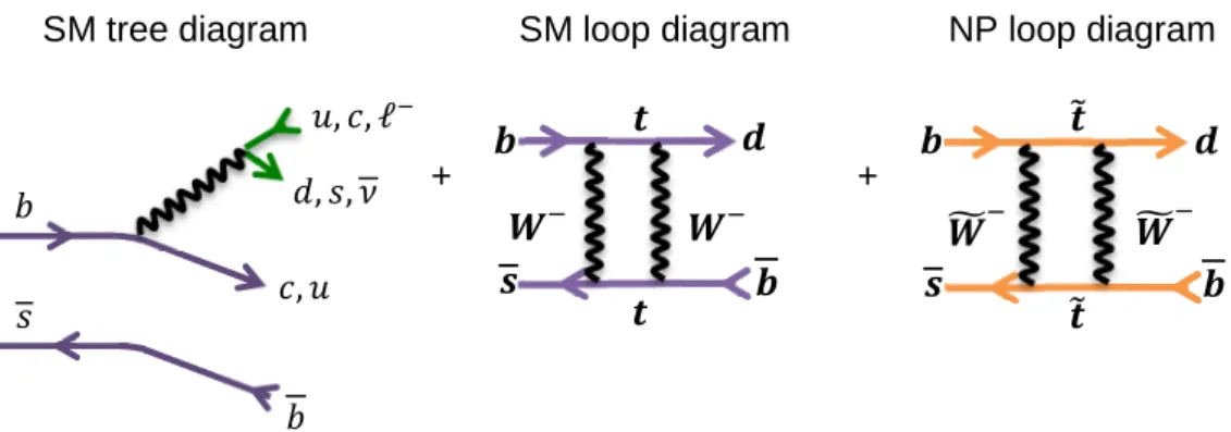
As an important tool for finding physics beyond the SM, flavor physics probes large mass scales via virtual quantum loops. FCNC, neutral meson-antimeson mixing and CP violation typically occur at the loop level in the SM. Precise measurements could potentially induce small NP virtual corrections. Hence this approach is also called indi- rect search for it infers NP through virtual contributions of new particles in processes involving only standard particles. It is based on high-statistics muon, kaon, tau, charm and B-meson production as well as precise measurements of SM parameters providing different constraints to individual processes. Experiments always measure the sum of SM and NP contributions. In order to set limits or to extract signals from NP it is indis- pensable to fully understand the underlying SM contribution. A widely accepted para- digm is that tree-level diagrams are dominated by SM processes, whereas loop dia- grams can be strongly influenced by NP [12]. An example is given in Figure 2-4.
SM tree diagram SM loop diagram NP loop diagram
+ +
Figure 2-4: Example of an SM standard process and 1st order loop corrections
!
"
#
#
! "
$, &, ℓ (, ), *
&, $ )
+
+
Both loop diagrams would add in the amplitude and hence interfere. The inclusion of NP particles with mass exchanged at the tree level with (1) coupling constants gNP/g would go well beyond the LHC energy scale [9]. Even if NP particles are exchanged only at 1-loop order the mass reach can be as high as (1TeV/c2) if minimal flavor violation (MFV) is assumed [13], and up to (100TeV/c2) if flavor violation couplings are enhanced compared to the SM [11]. The scope of the two approaches in searching for NP is depicted in Figure 2-5.
Figure 2-5: Sensitivity to New Physics as a function of the flavor violating couplings relative to the SM in the indirect searches at KEKB/SuperKEKB and direct searches at LHC/Tevatron [14].
In general if NP appears at the TeV scale in LHC experiments, SuperKEKB could measure its flavor- and CP-violating couplings or set independent constraints on the NP Lagrangian [15]. A comparison of SuperKEKB with LHCb unveils that the strengths of the two experiments are largely complementary [9]. At LHCb the expected yield for decay processes like B K*µµ, Bs φφ and B φKs should be substantially higher [16] because of the very large production cross section for b-quarks. This allows for example, extensive studies on Bs meson oscillations. On the other hand SuperKEKB provides a much cleaner environment which is essential for the exact measurement of CKM matrix elements, rare decay modes with missing energy as well as other search- es for possible NP effects [2].
Colliders at Super Flavor Factories can form specific particles or their excitations with- out any associated particles in the form of resonances. As an example at the Υ(4S) resonance ---pairs are generated. This allows the full reconstruction of a B meson from its daughter particles. By this means one can infer the missing momentum at- tributed to the other B meson, which in turn is essential for the measurement of chan- nels including neutrinos in the final state.
2.2 BELLE II Detector System
Detectors employed in high energy physics experiments normally incorporate several types of detection techniques into one single detector system [17]. The Belle II detector system in Figure 2-6 shows also a general purpose spectrometer consisting of layers of sub-detector components, each designed to look for particular properties or specific types of particles, arranged in the typical “onion shell”-fashion [18, 19]:
Figure 2-6: Belle II Detector System
There are tracking devices recording position, arrival time and path of a particle, calo- rimeters that measure a particle’s energy, and particle-identification detectors using a range of techniques to pin down a particle's identity.
• VerteX Detector (VXD): positioned most closely to the beam pipe there are two layers of Pixelated Silicon Sensors (PXD) adjacently followed by four layers of double-sided Silicon Strip Sensors (SVD). Together this sub-system measures decay vertex positions with a combined impact parameter resolution of σz0 ~ 20µm [19]. The precise evaluation of position coordinates is necessary for the determination of the particle’s trajectory origin. These tracking detectors register tiny electrical signals that particles create traversing the detector. From the de- flection in a magnetic field the particle’s momentum can be derived. One of the main concerns for the Belle II collaboration is the detector performance in an environment with considerable higher background levels. Conservative esti- mates assume that the background hit rate will increase by a factor of 20 whereas the physical event rate will be about 50 times higher. In this respect
CsI(TI) EM Calorimeter
4 layers double sided Si Vertex Detector:
2 layers PXD (DEPFET) 4 layers DSSD
Central Drift Chamber
Muon Detector KL counter
Particle Identification Device (PID)
the addition of a pixel detector is essential since results from current flavor fac- tories have proven high precision vertex reconstruction as a powerful tool to measure CP violation observables [20].
• Central drift chamber (CDC): the VXD is surrounded by a small-cell drift cham- ber (r = 16 – 112 cm) which measures trajectories, momenta and dE/dx infor- mation of charged particles. Additionally, it is used as trigger source and as a particle identification device for low momentum tracks.
• Particle Identification Device (PID): located just outside of the CDC in the barrel and end cap regions and principally7 designed to improve the K/π separation capability of the detector [10]. They are of the Cherenkov type with very fast read-out electronics. In the barrel region the formerly used ARICH counters are replaced by Time-Of-Propagation (TOP) counters allowing to measure the propagation time of the Cherenkov light emitted from charged particles passing through quartz radiator bars. In order to identify charged particles over the full kinematic range this detector sub-system also includes a forward end cap RICH with an aerogel radiator.
• Electromagnetic calorimeter (ECL): photons generated by collisions at the Υ(/) energy regime span a wide energy range from 20 MeV to 4 GeV, hence a high resolution electromagnetic calorimeter is essential for the precise determi- nation of the photon energy and angular coordinates. It contains a total number of 8736 CsI(TI)-scintillator crystals with different shapes in the barrel and end cap region located inside a Superconducting Solenoid Coil that provides a 1.5 Tesla magnetic field.
• KL/Muon (KLM) Detector: the outermost detector sub-system is instrumented to detect 12 mesons and to identify muons. It consists of an alternating “sandwich”
of 4.7-cm thick iron plates8 and glass-electrode Resistive Plate Chambers (RPC) in between. Since RPCs in the innermost layers of the KLM detector show unsatisfactory performance in the end cap region because of the ex- pected high background, they are replaced with scintillators.
There are many other factors influencing the performance of the Belle II detector sys- tem. Especially worth mentioning are a fast and reliable Triggering scheme (TRG), a Data Acquisition system (DAQ) recording collision events of interest upon trigger level- 1 and a grid-based distributed computing facility for data processing, MC production and physics analysis.
7 Providing also discrimination between pions, kaons and electrons below 1 GeV/c
8 serving as stopping material and as the magnetic flux return for the solenoid
2.3 SuperKEKB injection scheme
2.3.1 Principles of particle acceleration
In order to accelerate particles in a synchrotron and to compensate for energy losses due to the emission of synchrotron radiation a longitudinal electric field is needed. Ra- diofrequency (RF) cavities9 along the beam pipe use an oscillating voltage, so the par- ticle senses an accelerating electrical field in the cavities. To ensure that a charged particle always receives an accelerating force within the cavity, the RF frequency must be an integer multiple of the particle’s revolution frequency [21]:
ℎ(4567) ℎ8794& $+7 :; <7=$&>
7?9$549 <7=$&> (2-1) At SuperKEKB the planned RF frequency basis clock is 508.89 MHz. With a circumfer- ence of 3 km the harmonic number for electrons at the speed of light gives about 5120 points.10 The segments of the circumference centered on these points are called RF buckets. Electrons within the RF buckets get lumped into bunches.11 Each bunch con- sists of 1011 positrons or electrons. The particle density within a bunch is not homoge- neous but looks like a 3-dimensional Gaussian distribution.
The electrons in a bunch oscillate longitudinally around the equilibrium position, keep- ing the longitudinal size of the bunch stable. These oscillations are called synchrotron oscillations [18].
The electrons and positrons are guided in SuperKEKB by magnetic dipole fields around circular orbits, but move sinusoidally in both horizontal and vertical planes under focus- ing magnetic quadrupole fields around the design orbit. These periodic lateral move- ments are called betatron oscillations.
2.3.2 Beam Parameters increasing Luminosity
SuperKEKB is an asymmetric collider with a planned target luminosity of ℒ 8A10DE&)F, about 40 times as high as its predecessor KEKB [22, 23]. The range of beam energy covers the Υ(1/) and Υ(6/) resonance states for the physics opera- tion. By definition luminosity12 is related to the rate of particle collisions, consequently it is crucial for the production of meaningful quantities of rare events. The number of de- tected events H depends on the process cross section I usually measured in femto-
9 metallic chambers containing an electrical field in order to accelerate charged particles
10 with this number one can calculate the bucket length of ≈59 cm, which has to be compared with a bunch length of just 5-6 mm at SuperKEKB
11 this represents also an upper limit for the number of bunches within the collider (at Belle II only every second bucket gets filled with electrons resulting in 2503 bunches altogether)
12 luminosity can be interpreted as the beam focusing ability of the machine at the interaction point
barns13 (fb) or picobarns (pb), the luminosity ℒ controlled by the beam parameters of the collider and the detector efficiency J including trigger efficiency:
(H
(5 ℒ ∙ I ∙ J (2-2)
The event rate HLM of a specific process is given as:
(HLM
(5 ℒ ∙ ILM∙ -7 ∙ J (2-3)
where -7 is the branching ratio, i.e. the fraction of events for a chosen particle meas- ured to decay in a certain way14 and ILM the cross-section dependent on the specific physics process only. Unfortunately with higher luminosity new phenomena emerge at the interaction point (IP) [24]: dynamic beta effects and disruption are just some of them and will not be further covered in this thesis.15
In common textbooks luminosity for two transverse Gaussian beam distributions collid- ing head-on with equal beam sizes is defined as
ℒ <HFH
4IO∗IQ∗ (2-4)
where < is the bunch collision frequency, HF, the number of particles per bunch in beam1,2 and IO,Q∗ 16 is the beam size at the IP in the horizontal and vertical plane.
When the vertical beta functions of both beams are equal, the luminosity can be alter- natively expressed by beam parameters (2-5) [25]:
ℒ R±
27L1 +IQ∗
IO∗ V±WQ±
XQ∗ :2
:YQ± ∝[±\]±
^]±∗ (2-5)
where the subscript ± denotes positrons and electrons, R± is the Lorentz factor, is the elementary electric charge, 7L is the classical electron radius, V is the beam current, W±
is the vertical beam-beam parameter, XQ±∗ is the vertical beta function, :2 and :YQ± are geometrical reduction factors for the luminosity and the vertical beam-beam tune-shift parameter, respectively, owing to the finite crossing angle and the hourglass effect.
Other factors like the horizontal beta function at the IP, the horizontal emittance _OQ, the bunch length and the crossing angle between two beams not directly appearing in
13 1 barn = 10-28 m2
14 the sum of branching ratios for a particle is 1
15 the high density of compressed particles provides strong electromagnetic fields viewed by the particles of the incoming beam and this would bend particle trajectories (disruption)
16 the star indicates the minimum value
the formula are contributing to the luminosity through the beam-beam parameter [26].
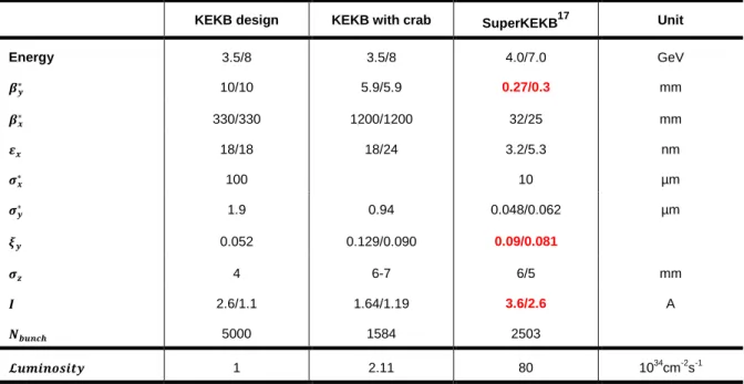
Table 2-1 gives an overview of some key design parameters for KEKB/SuperKEKB.
KEKB design KEKB with crab SuperKEKB17 Unit
Energy 3.5/8 3.5/8 4.0/7.0 GeV
^]∗ 10/10 5.9/5.9 0.27/0.3 mm
^`∗ 330/330 1200/1200 32/25 mm
a` 18/18 18/24 3.2/5.3 nm
b`∗ 100 10 µm
b]∗ 1.9 0.94 0.048/0.062 µm
\] 0.052 0.129/0.090 0.09/0.081
bc 4 6-7 6/5 mm
[ 2.6/1.1 1.64/1.19 3.6/2.6 A
defgh 5000 1584 2503
iejkfl k] 1 2.11 80 1034cm-2s-1
Table 2-1: Comparison of some of the key parameters of the SuperKEKB and KEKB designs [25]. Figures in bold red indicate three fundamental parameters determining luminosity.
2.3.3 Nano beam scheme
From equation (2-5) one can infer that the luminosity is sensitive to only three funda- mental beam parameters:18
• increase the beam currents (V±),
• make the electromagnetic beam-beam interactions small or equivalently in- crease the beam-beam parameter mWQ±n which is inversely proportional to the beam emittance [27] and
• reduce the vertical beta function mXQ±∗ n which addresses the focus of the beams at the interaction point [28].
Beam currents at SuperKEKB will be doubled in comparison with KEKB thus obtaining a luminosity gain by a factor of 2. Further current increases are not recommendable because of the electron cloud effect in the positron ring, high power costs and much higher detector backgrounds.
Regarding the beam-beam parameter, experiences from various colliders show that this value is limited to about 0.02-0.1. At SuperKEKB a maximum of 0.09 is assumed which has been already achieved at KEKB.
17 as of 2013/July/29
18 as an intermediate step KEKB scientists have installed crab cavities kicking the head and tail of each electron bunch so that the bunches made effective head-on collisions at the interaction point instead of crossing at an angle of 1.3 degrees (crab crossing improved the luminosity by 15%)
The most important luminosity increase will be achieved with a concept called “nano beam scheme” first proposed by scientists planning for the ILC [29]. The principal idea behind the nano beam scheme is to make the bunches very flat19 in this way raising the collision probability. At SuperKEKB the vertical beta function XQ∗ will be compressed by a factor of 1/20 of KEKB to just a few hundred microns at most. The new design will need strong final focusing quadrupole magnets placed closer to the interaction region to squeeze the beam into narrower bunches. However, this cannot be done arbitrarily small because of the hourglass effect. To minimize the hourglass effect for conven- tional head-on collisions the beta function has to be larger than the bunch length ~5mm mXQ∗ o Ipn. By contrast the nano beam scheme requires XQ∗ ostu vqr∗ disclosing a propor- tional dependence on the horizontal spot size and an inverse dependence on the half crossing angle w. Accordingly the crossing angles will be substantially enlarged from 22 mrad to 83 mrad and the bunches only intersect at the highly focused regions with effective bunch length ( stu vqr∗ shown in Figure 2-7.
Figure 2-7: Comparison of different Collision Schemes (schematic view)
In order to implement the new scheme effectively a lot of former used items of the KEKB collider have to be upgraded [25]. First of all the lattice design, which represents the arrangement of the magnets along the beam path for guiding and focusing the elec- trons and positrons has to be updated. The magnet system in accelerators consists of various types like dipoles used for bending, quadrupoles used for focusing (focusing in one plane, and defocusing in the other) and sextupoles used for chromatic corrections.
The combination of different magnets into building blocks constitute the lattice design resembling a complicated optical system with FODO cells (focusing & defocusing quadrupoles), double bend achromat (DBA), triple bend achromat (TBA) or other multi bend achromat types. For SuperKEKB the quadrupole magnets of KEKB will be reused as much as possible, the dipole magnets will be replaced by shorter ones and the peri- od of the wiggler magnets will be reduced to half of that of KEKB by adding new ones.
As already mentioned the final focus section was completely redesigned to achieve an extremely low beta function at the IP. By rearranging, replacing and adding magnets
19 one might think of steamrolled spaghettis
the beta functions and dispersions will be modified. As a countermeasure against elec- tron cloud issues the beam pipes in the LER arc section will be replaced with new alu- minum-alloy pipes with antechambers. To reduce the emittance of the electron beam a photo-cathode RF low-emittance electron gun will be installed. The emittance of the positron beam will be minimized by a new damping ring. The overview of the upgrade to SuperKEKB is shown in Figure 2-8.
Figure 2-8: Overview of upgrade to SuperKEKB [25]
2.3.4 Beam life time and dead-time during injection
Due to various energy loss effects (see below), some of the particles deviate from the prescribed path along the vacuum tube and interact with the beam pipe thereby creat- ing particle showers which may reach the detector. The number of particles lost in an accelerator is proportional to the number of beam particles [30]:
(H xH(5)(5 (2-6)
where x is a constant. Defining the beam lifetime as y 1/x, then the beam current V decays as
V V∙ {| (2-7)
In general, beam losses mainly arise in the collimation area or on other aperture limits.
Basically five beam loss processes are observable [31]: first, betatron or synchrotron oscillations intensify the quantum emission thereby increasing the tails of the bunch distribution. Next, the intra-beam scattering dominated by the Touschek effect, and the beam-beam background appearing at the IP when the colliding beam particles un- dergo scattering via radiative Bhabha processes. Finally, elastic and inelastic scatter- ing with residual gas molecules in the vacuum tube.
The individual loss mechanisms contribute to the total beam lifetime as [32]:
1
y 1
y}~u~+ 1
y~sL + 1
yLL+ 1
yLst+ 1
ytuLst (2-8)
As a result the total beam lifetime will always be less than the value of the smallest lifetime input. The most dominant beam loss contribution stems from the Touschek effect. The stability of the trajectories highly depends on the amplitudes of betatron and synchrotron oscillations. If these oscillations are outside the longitudinal or transverse acceptance of the storage ring the particles are lost. In this respect it is customary to define dynamic aperture as the maximum phase-space amplitude within which particles do not get lost after a certain amount of turns20 [33]. In other words, dynamic aperture sets an amplitude threshold for the motion of charged particles. At SuperKEKB it is estimated numerically with six-dimensional tracking simulations using a specific pro- gram for optics design and particle tracking. As a result the dynamic aperture is rather small compared to KEKB inducing a larger background and consequently a shorter lifetime of the beam. The intra-beam scattering rate (“Touschek effect”) per particle depends on the following parameters [34]:
(:85) ∝ H
D∙ I (2-9)
where H stands for the number of particles per bunch, for the beam energy and I represents the transverse beam size. As already mentioned most of the luminosity in- crease at SuperKEKB comes from a significant reduction of the beam size. A twenty- fold compression of the bunches significantly rises the likelihood of intra-bunch cou- lomb scattering. By implication this increases the amplitudes of particles that will be either absorbed at the collimation area or collide with the beam wall. Accordingly, the dominant particle loss mechanism21 at Belle II will be the Touschek effect reducing the LER beam lifetime significantly from 150/200 min as in the KEKB case to just 10 min.
As a consequence the bunches have to be replenished continuously. This is done by injecting two “daughter bunches” 100 ns apart into the LER and HER respectively at a total frequency of 50 Hz. The pair of daughter bunches are selected by bunch current monitors, and the pair with the smallest bunch current sum is chosen to be topped off in the next injection.
20 1000 turns at SuperKEKB with synchrotron oscillation but without quantum excitation (radiation damping)
21 the loss rate due to scattering with gas molecules is lower by a factor of 3-4
Figure 2-9 and Figure 2-10 give an overview of the injection scheme for SuperKEKB with the septum magnets for bunch injection.
2503 bunches
… …
118 cm
100 ns
Figure 2-9: SuperKEKB bunch train.
20 µs frame
~cooling: 4 ms noisy ~16 ms clean
Figure 2-10: Injection Scheme of SuperKEKB
Now the problem emerges that these daughter bunches are located further away from the orbit of the corresponding main bunches and therefore are subject to large ampli- tudes in their betatron oscillations. They are naturally cooled down by synchrotron radi- ation within a certain damping time. During this time the particles in the daughter bunches are more likely to collide with the bream pipe in the vicinity of the interaction point, creating additional background. The daughter bunches are therefore often called
"noisy bunches". At KEKB the damping time was 4 ms and this number will be also assumed for SuperKEKB. The noisy bunches will pass the detector every 10 µs. For the PXD (see chapter 3.5) the detector readout cycle was determined at 20 µs which means that all signals registered within the 20 µs between two readout cycles are
2nd noisy bunch 1st noisy
bunch
Belle II
stored (integrated). As a worst case this would mean that all frames recorded during the cooling period have to be discarded. This would substantially raise the dead-time of the detector to 20% or in other words produce a loss of two years time assuming a typ- ical operational period of 10 years. Many proposals have been made to overcome this problem, for example a faster read-out (4-fold ganging), decreasing the injection rate while injecting 4 bunches instead of 2, synchronize injections from LER and HER or reducing damping time. But these alternatives are either too costly or not feasible from the current technical status. Fortunately the PXD used at Belle II offers a lot of amazing features especially the possibility to gate the detector during the passage of the noisy bunches. Its modalities, operation principles and the design will be described in the next section.
3 DEPFET Sensors
Flavor physics sets high standards on precision measurements requiring a spatial reso- lution of a few ten of microns in order to measure the decay vertices of the two B me- sons produced at the Υ(4/) resonance. At Belle II a specific condition for detector reso- lution is the measurement of the decay time difference of the B meson and its anti- particle, expressed in their mean flight distance of Δz ≈ 130 . A derivation of this figure can be found in the Appendix A.
To safely distinguish two different vertices the vertex resolution has to be one order of magnitude better than the distance between the vertices [35]. Only silicon detectors can meet the challenge of acceptable resolution combined with a fast readout. How- ever, the double sided silicon strip detector (DSSD) as innermost detector used for Belle cannot cope with the much higher event rate at SuperKEKB together with the higher background22, which would lead to a large strip occupancy making vertex re- construction of B-decays impossible. For that reason it was decided to upgrade the new Belle II detector system with a pixel detector. The combined PXD and SVD impact parameter resolution at Belle II will be at Ip ≈ 20 .
There are fairly different pixel detector architectures under consideration all having ad- vantages and drawbacks [36]. CCDs suffer from relatively slow read-out speed and continuous sensitivity distorting the measurements during the transfer cycle. In contrast hybrid pixels used for the ATLAS detector at CERN are very fast (25 ns read-out speed) but with their thick sensors and chip-integrated full read-out electronics they are too bulky for energy levels in the (1)area (multiple scattering because of relatively low particle momentum). A very promising and highly innovative technology are mono- lithic active pixel sensors (MAPS) incorporating standard CMOS technology in a p-type epitaxial layer on a high resistive n-type substrate [37]. Because of their low intrinsic capacitances these devices have excellent signal to noise ratios. On the other hand the charge collection times are still too long. Nevertheless the idea of integrating readout electronics into a single monolithic device will influence the construction of detectors in future high energy experiments. In contrast DEPFET detectors seem to be actually best-suited for high precision vertex pixel detectors [38]. They avoid most of the above shortcomings having low mass and offering intrinsic amplification and adequately fast readout times. Furthermore power consumption can be kept very small saving addi- tional cooling material.
22 the beam pipe radius shrinks to about 10 mm, so the detector can be put closer to the IR, which is good news for vertex reconstruction; on the other hand the background increases substantially since is propor- tional to the inverse square of the radius
3.1 DEPFET Operation
3.1.1 The DEPFET Principle
The idea for DEPFET detectors was proposed by two Munich scientists J. Kemmer and G. Lutz in 1987 [39]. The technology was developed by the Semiconductor Laboratory (HLL) of the Max Planck Society in Munich. DEPFET detectors integrate signal detec- tion and first amplification in a single silicon pixel structure, so that the position meas- urement of traversing particles can be achieved with a minimum of material. The sen- sor consists of a depleted p-channel MOSFET implanted onto the surface of a high- resistive n-doped silicon substrate and a p+ implant at the backside. More about semi- conductor devices can be found in common textbooks like [40, 36], MOSFETs are comprehensively described in [41].
The substrate is fully depleted by means of sideward depletion as depicted in Figure 3-1. This is established by applying negative voltages to the source p+ and back con- tact p+ relative to the bulk potential n+ (a). If the voltages applied on both p+ contacts are sufficiently strong and equal, the depletion layers will meet in the center of the sub- strate (b) creating a potential minimum for the electrons. By relatively varying back and front side voltages, the minimum is shifted up vertically right below the top surface of the bulk substrate (c).
Vfront = Vback < 0V
(a) E-field Potential
Vfront = Vback << 0V
(b)
E-field Potential
Vfront < 0V
(c) E-field Potential
Vback << Vfront << 0V
p+ n+ n metal depleted
Figure 3-1: Concept of sideward depletion. Two p-n junctions share the same bulk con- tact. The n-bulk is grounded by means of a n+ electrode. The electrical field and the parabolic potential curves for different voltage settings are displayed on the right.
The full depletion voltage L of an n-type bulk together with a highly doped p+ region is directly proportional to the quadratic sensor thickness ( [36]:
L+ t =
2__(HL (3-1)
with t the built-in voltage representing the potential difference across the p-n junction in equilibrium, = the elementary charge, _ the vacuum permittivity and _ the relative permittivity of silicon and the effective doping concentration HL∙
with H, H
the acceptor and donor concentrations.
The position of the potential minimum tu can be derived solving the one-dimensional Poisson equation with the given boundary conditions m(0) u, (() n [42]:
tu ( 2 + __
=H( m un (3-2)
where it was assumed that the acceptor concentration is much larger than the donor concentration H ≫ H. u label the voltages of the back and front side p+ electrodes.
Figure 3-2: Left: cross section of DEPFET pixel with a minimum ionizing particle creat- ing 80 electron hole pairs per µm for a 75 µm thick sensor. The electrons are attracted by the internal gate, the holes drift to the p+ back contact. Right: PXD6 standard proto- type design view on polysilicon and implanted layers (beige – first Poly (Cleargate), yel- low – second Poly (Gate), brown – p-type implant (source, drain, drift), green – n-type implant (Clear). High Energy (HE) implants are used to increase the lateral drift field [43].
By an additional phosphorus n doping a potential minimum, called internal gate, is shaped at 0,65 µm below the Gate oxide of the transistor channel. This deep doping implant occupies only a tiny fraction of the pixel volume.23 At depletion all free electrons are removed from this area leaving back a positive space charge remaining highly at- tractive for electrons. Now the detector volume is sensitive to incident radiation produc- ing electron-hole pairs. Applying an electric field to the pixel separates the holes which drift to the negatively biased backplane whereas the electrons are collected in the po- tential minimum. High accumulated charges in the internal gate can neutralize the in- ternal gate potential leading to an insensitive detector. To avoid this effect the electrons are regularly removed by applying a positive voltage to a Clear contact as explained in chapter 3.1.4
3.1.2 Electrical properties of DEPFET devices
The accumulated charge in the internal gate changes the potential and thus modulates the current24 of the MOSFET channel if it is switched on. The source-drain current with empty internal gate is called pedestal current VL. If electrons are stored in the internal gate after an ionization event an additional signal current Vst¡will be generated. To
among many other parameters on the external gate structure, doping concentration and varies its size dynamically with the amount of charged electrons
24 in electrodynamic terms the charge stored induces mirror charges in the external transistor
MIP
measure the signal current the pedestal current has to be subtracted from the total transistor current.
Vst¡ Vst¡L VL (3-3)
This signal current represents the first amplification stage of the DEPFET sensor. Its amplitude is proportional to the number of collected electrons in the internal gate. The internal amplification 6} is defined as change of the transistor current ∂V£ as a function of the internal gate charge ∂¤st¡ at constant Gate-Sourceª£ and Source-Drain voltages
£ [43]:
6} ∂V£
∂¤st¡®
¯°±,¯±
(3-4) typically given in ²³/. It is now possible to determine the amount of charges accu- mulated in the internal gate. The electrical characteristics of DEPFET transistors are very similar to that of standard MOSFETs. The main difference concerns the space charge region below the channel. In case of a standard MOSFET this region extends up to the undepleted bulk whereas for the DEPFET the region between channel and internal gate potential is relevant. The latter changes its potential depending on the amount of stored electrons. Due to parasitic couplings to other regions25 [44] of the pixel structure not all but a fraction < of the charge will be induced in the channel. With the approximation that this induced charge is uniformly spread over the channel, an internal gate charge is equivalent to an external Gate voltage change by an amount of26
´ª£ < ∙´¤st¡
µª (3-5)
with µª ¶ ∙ · ∙ µO the Gate-channel capacitance, W and L denoting the width and length of the transistor and µO º»rº
»r the oxide capacitance per unit area depending itself on the dielectric constant _O and the width of the oxide (O. For a DEPFET de- vice, which is operating in the saturation region under the condition ¼½±
¼¯± 0, the cur- rent-voltage characteristics become:
£,s < ∙¤st¡
µª + ª£,L (3-6)
ª£,L ª£ (3-7)
25 neighboring electrodes like backside contact, source and drain
26 a derivation of the following formulas can be found in [32]
V£,s V£m£,sn 
· µO£,s
2 (3-8)
6},s ´V£,s
´¤st¡
· <µO
µª £,s <¾ 2
¶·DµO¿V£,s (3-9) with being the hole mobility and the transistor threshold voltage expressing the minimum Gate-Source voltage needed to create a conducting path between source and drain terminals. From equation (3-9) one can easily derive the following dependencies of the internal amplification keeping all other parameters constant in each case:
6} ~ 1
·D ⁄ , 1
¶F ⁄ , ¿(O , ¿V£,s (3-10)
For Belle II applications the internal gate can store about 40,000 electrons without any degradation of the linear response. Injecting more electrons could make the MOSFET channel conducting even when the Gate voltage is in off-state. This process saturates at about 60,000 electrons due to charge overflow [43]. The 6}-value for a Gate length of
· 6 and a V£ 100³ used in this study is about 400 ²³/ [44].
3.1.3 Readout of DEPFET Pixel Matrices
The readout process of a single DEPFET pixel follows an iterative loop [37]:
a. Sampling: pixel is in off-state and remains sensitive to ionizing particles. The generated electrons will accumulate in the internal gate.
b. Readout: switching on the transistor by applying a voltage to the external Gate. The source-drain current, composed of Vst¡L is measured. The signal is cal- culated by subtracting a stored pedestal value, which was determined before during a dedicated pedestal measurement. This strategy is also referred to as single sampling. At an earlier stage a double correlated sampling was consid- ered equivalent to an extra pedestal measurement directly after erasing the sig- nal via a Clear process. However, balancing signal quality against readout speed the collaboration opted for the latter.
c. Clear: a voltage pulse is applied to the Clear contact, removing the collected charge completely from the internal gate.
d. Reset: set external Gate voltage in off position, which switches off the transistor.
Sampling charge continues.
The whole matrix operation is characterized by low power consumption27 as the transis- tors are turned off during charge collection.
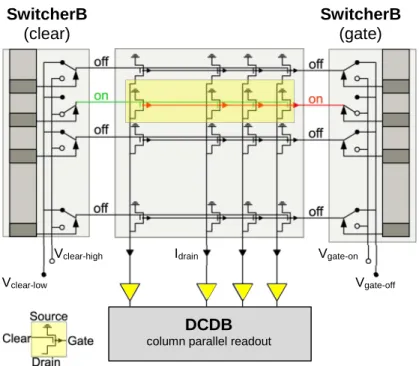
The DEPFET pixels can be arranged in a two-dimensional matrix structure. All transis- tor drains of a column are connected in parallel to the amplifier nodes of the DCDB.
The Gate and Clear contacts are connected row wise and steered by the SwitcherB. To increase readout speed, four pixel rows are connected together, so they are collectively switched on/off and erased at the same time. This in turn quadruples the drain lines:
four drain lines for the readout of four rows of one pixel column are needed. As a result the pixels in the same column are read out sequentially, while pixels in the same row are read out in parallel. This is known as rolling shutter mode: one electrical row = 4 physical rows. The rows are switched on by applying the GateOn voltage and all pixels of that row are read employing the sample-clear-sample cycle described above. Then these four rows are switched off and the next four rows are turned on for readout until all rows have been read and the cycle starts again.
Figure 3-3: Schematics of DEPFET sensor operated in rolling shutter mode. The rows are activated sequentially by the SwitcherB chip. The drain currents are transmitted in parallel to the DCDB for further processing. Before switching to the next row (or set of rows) the Clear pulse is applied (Gate and Clear function are physically implemented into one chip).
The measurements for this thesis were performed with a rather small matrix structure consisting of 64 rows and 32 columns with a total of 2,048 pixels, each covering a sur-
27 for an average current of 100 µA a DEPFET half ladder only consumes 0.5-1 W in the sensitive area and 9 W in total, mainly due to the readout electronics at the end of stave; accordingly air cooling is suffi- cient [38] [95]
DCDB
column parallel readout
SwitcherB (clear)
SwitcherB (gate)
Vgate-off
Vclear-low
Vgate-on
Vclear-high Idrain
face area of 50x75 µm2. This has to be compared with a half ladder of the PXD com- posed of 768 rows and 250 rows with a total of 192,000 pixels.
3.1.4 ClearClearClearClear Process
In contrast to many other sensor concepts the collected charge will not be erased dur- ing the readout of the DEPFET pixels, so the measurement is non-destructive. This allows in principle multiple readouts for the same signal. However, leakage current and signal charges can quickly fill up the internal gate. We will see later that even a relative- ly weak laser pulse easily shifts the internal gate of many pixels into saturation, subse- quently preventing further charge collection.
Without radiation damage28 leakage currents will be negligible small for the BELLE II PXD. Former analysis on a 450 µm thick DEPFET sensor measured 600 electrons that accumulated in the internal gate within a time interval of 0.8 ms [45]. Taking into ac- count the much shorter integration time of 20 µs this translates to only about a dozen leakage electrons, a factor of ten below the sensitivity threshold of the DCDB for 1 ADU (=73nA).29
To preserve the sensitivity of the sensor, the charge must be removed regularly from the internal gate. This process is called Clear. The Clear region is an n+-implantation in the substrate shared by 4 DEPFET pixels. It is placed peripherally on both sides of the internal gate to facilitate a very fast Clear process. Applying a positive voltage to the Clear contact induces electrons to flow from the internal gate to the Clear. The entire charge of the internal gate can be removed with a sufficiently strong and long Clear pulse called “Complete Clear”. If a residual charge remains in the gate, this would rep- resent an additional source of noise.
HLL together with the Weierstrass Institute have performed extensive 3D-simulation studies on how to structure the DEPFET pixel drift fields30 in order guide the electrons directly to the internal gate. A special mechanism prevents a competition between in- ternal gate and Clear in the course of the charge collection phase: during charge collec- tion the Clear contact is put on negative potential compared to the substrate and a fur- ther deep boron p+-implantation, called p-well, is introduced shielding the Clear contact from the internal gate. However, this implantation introduces a new potential barrier, making the process of clearing more difficult. To control the p-well and the potential of the substrate neighboring the internal gate, a Cleargate structure has been implement- ed [46]. Besides serving as a potential barrier the Cleargate supports the Clear process if the Cleargate voltage is raised during the Clear process.
28 in case of radiation damages this is no longer true but can be kept under control via cooling
29 1 ADU corresponds to an internal gate charge of at least 180 electrons (assuming an internal amplifica- tion of 400 ²³/)
30 vertically the electrons move within a few nanoseconds to the local potential minimum however, since the lateral drift fields are weaker the whole process takes between 50-60 ns depending on the drift voltage
![Figure 3-8: Elements of the PXD data transmission system [57]](https://thumb-eu.123doks.com/thumbv2/1library_info/4011669.1541185/36.892.189.746.577.978/figure-elements-pxd-data-transmission.webp)
![Figure 3-10: Block diagram of one DCDB pipeline analog channel with several building blocks explained in the text [63]](https://thumb-eu.123doks.com/thumbv2/1library_info/4011669.1541185/39.892.182.760.99.618/figure-block-diagram-pipeline-analog-channel-building-explained.webp)