The Wide Field Imager of the European X-Ray Observatory
Peter Lechner, Ladislav Andricek, Klaus Heinzinger, Sven Herrmann, Nils Kimmel, Thomas Lauf, Gerhard Lutz, Rainer H. Richter, Matteo Porro, Gerhard Schaller, Martina Schnecke,
Florian Schopper, Heike Soltau, Lothar Strüder, Johannes Treis, Stefan Wölfel, Zhang Chen
Abstract – The European X-ray Observatory (XRO) also denoted as X-ray Evolving Universe Spectroscopy (XEUS) mission is currently under assessment by the European Space Agency as a follow-up to XMM-Newton and Chandra with an intended launch date around 2015. XEUS/XRO aims to place an X-ray telescope in space with an aperture comparable to the largest ground based observatories. The large collecting area sets new frontiers for the focal plane instrumentation in terms of sensitive area, spectral and spatial resolution and readout speed.
To cope with the challenging requirements of the XEUS/XRO Wide Field Imager a new type of Active Pixel Sensor based on the integrated amplifier DEPFET (DEpleted P-channel Field Effect Transistor) has been developed and characterized. This concept combines excellent energy resolution, high speed readout and low power consumption with the attractive features of readout on demand and random accessibility of pixels. A first series of prototype devices produced and characterized at the MPI semiconductor laboratory in Munich/Germany already meets most of the XEUS/XRO specifications. A second generation of devices with substantially larger formats is currently in production. Other device concepts and operation modes derived from the DEPFET principle are introduced.
I. THE EUROPEAN X-RAY OBSERVATORY
In the continuing long-term science program 'Cosmic Vision, Space Science for Europe, 2015 - 2025' [1] the European Space Agency (ESA) emphasizes the significance of a large aperture X-Ray Observatory (XRO), also denoted as XEUS (X-ray Evolving Universe Spectroscopy). Built on the successes achieved with ESA's XMM-Newton and the US (RXTE and Chandra) and Japanese (ASCA and Astro-E2) space observatories the XEUS/XRO mission is targeting some of the yet unresolved issues of high-energy astrophysics concerning the early stage of the universe and matter under extreme conditions:
Manuscript received November 6, 2006. This work was supported by the European Space Research and Technology Centre ESTEC under contracts no.
14807/00/NL/NB and 15851/01/NL/HB.
K. Heinzinger, P. Lechner, H. Soltau are with PNSensor GmbH, Römerstr. 28, D-80803 München, Germany (author's contact: telephone:
+49-89-83940051, e-mail: peter.lechner@pnsensor.de).
L. Andricek, Gerhard Lutz, R. H. Richter and M. Schnecke are with the Max-Planck-Institut für Physik, D-80805 München, Germany.
S. Herrmann, N. Kimmel, T. Lauf, M. Porro, G. Schaller, F. Schopper, L. Strüder, J. Treis, S. Wölfel, and Zhang C. are with the Max-Planck-Institut für extraterrestrische Physik, D-85741 Garching, Germany.
All authors are in addition with the MPI Halbleiterlabor, Otto-Hahn- Ring 6, D-81739 München, Germany (telephone +49-89-8394000).
Zhang Chen is in addition with the Tsinghua University of Beijing, China.
• find the very first gravitationally bound structures assembled in the universe and follow their evolution towards today’s galaxies, groups and clusters,
• investigate the formation and evolution of the super- massive black holes at galactic centers in relation to galaxy and star formation,
• trace the life cycles of chemical elements through cosmic history,
• study the spectral and time variability of the X-ray emission of matter in the strong gravitational field of black holes and neutron stars.
The variety of scientific tasks requires high sensitivity (several square meters collecting area) over a broad energy band (100 eV to 50 keV) with excellent energy resolution.
High spatial resolution (few arcsec) will be needed to avoid source confusion and good time resolution (few μsec) to probe the relevant timescales. The combination of the above stated specifications imposes a telescope with a large aperture of several m² and a large focal length of several ten meters.
Consequently, XEUS/XRO will consist of a Mirror Spacecraft (MSC) in formation flight with a separate detector spacecraft (DSC). The two spacecrafts are aligned by active control to provide an autonomous formation flight with a relative position accuracy of 1 mm3.
During its definition phase the XEUS/XRO mission scenario underwent several redirections. The initial configuration foresaw a multiple launch approach of the two spacecrafts to a low earth orbit utilizing the International Space Station ISS as a platform for the mirror mounting and for periodic DSC refueling. The mirror was still based on the XMM-Newton nickel technology and planned to be assembled by the ISS robotic arm to a final size of 30 m². The vague situation of both the ISS and suitable launch vehicles and a breakthrough in the development of light weight silicon high- precision micro-pore optics [2] favored the concept of a joint European/Japanese/NASA mission with a 10 m² self-deploying mirror launched together with the DSC to the Lagrange point 2 (L2) by a single Delta-IV-Heavy carrier. After NASA's decision to suspend the collaboration due to different model payload assumptions, the now consolidated XEUS/XRO scenario [3] is a more cost-effective mission including an ArianeV-ECA launch of MSC and DSC as a single stack to a halo orbit around L2. The mirror telescope is again based on silicon micro-pores in a conical approximation of the Wolter-I
2006 IEEE Nuclear Science Symposium Conference Record N44-2
geometry on a fixed cylindrical optical bench with a focal length of 35 m (fig. 1.). The effective area of about 5 m² at 1 keV is using the maximum diameter offered by the launcher fairing. By applying multilayer coating the usable energy range may be extended to 40 keV with an effective area of 0.1 m².
The angular resolution has been specified to be 5 arcsec half energy width (HEW) with a goal of 2 arcsec HEW, translating to a point spread function (PSF) of 850 μm and 340 μm in the focal plane.
II. THE XEUS/XRO PAYLOAD
The XEUS/XRO focal plane instrumentation is organized into the core payload that fulfills the main science requirements. In addition to the core payload, high priority augmentation instruments are defined which will be considered if resources allow.
A. The Core Instruments
The mission's fundamental scientific goals could be accomplished by a pair of complementary baseline instruments comprising one Wide Field Imager (WFI) and one Narrow Field Imager (NFI). The WFI is a silicon Active Pixel Sensor with a field of view (FOV) of 7 arcmin and an energy resolution of 150 eV (FWHM at 5.9 keV). Its working principle and status will be described in detail throughout the following sections. The WFI is foreseen to work as a pathfinder for the NFI which provides imaging spectroscopy capability between 0.2 and 6 keV on a FOV of 0.75 arcmin with ultimate spectral resolution (2 eV FWHM at 0.5 keV). At present two different NFI designs are under study:
• NFI-1 is based on an array of super-conducting tunnel junctions (STJ) [4], operated at a temperature of < 300 mK via a ³He sorption cooler.
• NFI-2 is based on an array of micro-calorimeters [5], operated at 50 mK via an adiabatic demagnetization refrigerator.
Given the early definition stage of the mission, a definitive choice on the actual NFI design has not yet been made and therefore both designs will be analyzed in the context of the currently performed XEUS/XRO payload accommodation study.
B. The Augmentation Instruments
The following instruments are to be considered in addition to the core payload should resources be sufficient.
• Narrow Field Imager (second unit)
• High Time Resolution Spectrometer (HTRS) [7], [8]
HTRS will use the telescope’s large aperture to collect X-rays emitted by time-variable objects with a periodicity in the msec range. These quasi-periodic oscillations in the X-ray emission are generated in the inner accretion flows around the most extreme compact massive objects, black holes and neutron stars, and carry information about regions of strongly curved space-time. In this regime important predictions of the theory of general relativity are still to be tested. HTRS is based on a monolithic array of silicon drift detectors (SDDs) capable to provide spectra with resolving power E/dE of 5 to 50 in the energy range 500 eV to 10 keV, at very high time resolution (10 μsec) and at very high count rates (2 MHz). To distribute the enormous photon flux uniformly over the sensor area HTRS will be displaced vertically in an out-of-focus position.
• Hard X-ray Camera (HXC) [9]
HXC will exploit the high-energy performance of the mirror telescope in multilayer coating technology to provide spectra with a resolving power E/dE of 10 % at energies
> 15 keV, simultaneously with images of a 5 arcmin FOV, and with time resolved photon counting. The HXC is based on a Cd(Zn)Te pixel array to be operated and placed in transmission mode behind the WFI sensor. In order to suppress background, an active anticoincidence shield is placed around the imager.
• X-ray Polarimeter (XPOL) [10], [11]
To investigate the emission mechanisms of AGNs and galactic centers XPOL provides polarimetric measurements simultaneously with spectral information with resolving power E/dE of 5 in the energy range 1 keV to 10 keV. XPOL is based on a gas proportional counter with very high spatial resolution by a micro pattern cell readout that is able to recognize tracks and hence ejection direction of the primary photoelectron.
The ancillary XEUS/XRO payload components will be selected on a competitive basis depending on the available resources which are currently under investigation within the frame of an industrial feasibility study of the DSC payload accommodation.
III. THE XEUS/XRO WIDE FIELD IMAGER
A. The WFI Science Requirements
After the revision of the consolidated mission the XEUS Science Definition Team defined the required performance of the payload instruments [12], [13]. For the Wide Field Imager
Fig. 1. Artist's impression of the XEUS/XRO mirror spacecraft (back) in formation flight with the detector spacecraft (front) at a focal length 35 m.
the good angular resolution of the XEUS/XRO telescope and the large throughput set demanding specifications.
• To detect X-ray luminous objects at high red-shift, which are expected to have a density of 1 per 5 arcmin section of the sky, and to provide sufficient background statistics the WFI sensor must cover a field of view of 7 arcmin translating to a sensitive area of more than 7 cm diameter in the focal plane.
• To limit source confusion and to resolve red-shifted objects the angular resolution must be a half energy width (HEW) of 5 arcsec with a goal of 2 arcsec corresponding to a 850 μm or 340 μm wide point spread function in the focal plane. A pixel size of 75 μm to 100 μm is adequate for the anticipated angular resolution to ensure that the spatial resolution is limited by the telescope rather than by the sensor and to avoid unnecessary over-sampling. For a pixel size of 75 μm about 70 % of all events with a typical charge cloud radius of 20 μm will be split events and 30 % are contained within one pixel. On those conditions, the position resolution will always be better than 20 μm, but for most of the cases better than 5 μm.
• To be able to detect on the one side super-massive black holes at extreme red-shift z ≥ 10 and to perform hard X-ray spectroscopy of matter in the strong gravity fields of neutron stars and black holes on the other side the WFI must provide efficient response in the energy range from 100 eV to 15 keV requiring a thin entrance window and a minimum sensitive thickness of 450 μm.
• Spectroscopy of relativistic distorted lines requires an electronic noise of 5 electrons ENC (equivalent noise charge).
• To avoid photon pileup the full frame readout time must be in the order of few msec. For instance, at a frame rate of 1000 Hz a source producing 1000 counts per sec on an area of 7 x 7 pixels can be detected with a pile-up probability below 2 % in full frame mode. To cope with high-intensity point sources a fast window mode must be implemented. For example, at 5 m² sensitive area a bright AGN (active galactic nucleus) with an intensity of 20 mCrab will give 8000 counts per sec. To observe such a source with < 1 % distortion of the spectrum by pile-up the readout system must provide the flexibility to define a window with a depth of 16 pixels at a
targeted readout time per pixel row of 4 μsec.
• The option of the Hard X-ray Camera detecting the energetic photons transmitted through the WFI implies that the WFI sensor must be a monolithic device without mechanical support structure below the sensitive area.
• Due to spacecraft constraints the WFI will have to operate at a temperature ≥ -60 °C and the power consumption in the focal plane is restricted to 20 W.
To unify the above stated specifications in a single device the new device concept of an Active Pixel Sensor (APS) has been developed, i.e. every pixel has its own integrated amplifier and can be addressed individually by external means.
The WFI sensor will have a format of 1024 x 1024 pixels with a pixel size of 75 μm x 75 μm equal to a sensitive area of 7.68 cm x 7.68 cm (fig. 2). It will be monolithically integrated on a 6-inch silicon wafer with a thickness of 450 μm to 480 μm. The sensor area is logically divided into 16 sub-units with a format of 128 x 512 pixels each to be readout in parallel. The proposed APS of the XEUS/XRO Wide Field Imager is based on the integrated sensor/amplifier structure DEPFET.
B. The DEPFET Principle
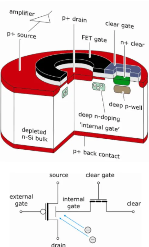
The DEPFET (DEpleted P-channel Field Effect Transistor) is a device with the combined functionality of detector and amplifier [14]. It consists of a p-channel field effect transistor on a high resistivity n-type silicon bulk. The transistor may be either a JFET or a MOSFET of enhancement or depletion type. For reasons of technological feasibility and reproducibility on large format devices the MOSFET-based device is usually the preferred design. The bulk is completely depleted by the reverse biased backside diode thus creating a potential minimum for electrons close to the surface. An additional deep n-doped region enhances the depth of the potential minimum and confines it in the lateral direction to the extent of the FET channel (fig. 3).
Each electron released in the depleted volume below the transistor by the absorption of ionizing radiation or by thermal generation will drift to the potential minimum and will be stored there. By inducing positive image charges inside the FET channel the stored electrons enhance the transistor current. Thus the DEPFET's current is a function of the amount of charges in the potential minimum, and its measurement yields information of the energy absorbed in the depleted volume. Because of the stored electrons' current steering function the potential minimum is called 'internal gate'.
Electrons accumulated in the internal gate must be periodically removed by applying a suitable high voltage to an n doped 'clear' contact adjacent to the internal gate. The clear contact acts as a drain for electrons and it is supported by an additional MOS 'clear gate'. For the reset, both the clear and the clear gate are set to a more positive voltage. The clear contact is shielded by a deep p-implanted well to avoid the direct loss of signal electrons during signal integration.
As the signal charges are confined in a potential well, the information is not destroyed during the readout, so that multiple readings with subsequent averaging are possible, thus reducing the noise contribution by the square root of the number of readings [15].
The internal gate exists, i.e. electrons can be collected and stored in it, regardless of a current flowing in the channel of the DEPFET or not. The transistor current is usually turned off during signal integration and only switched on via the external gate for the signal readout, thus minimizing power consumption. Unlike a conventional detector-preamplifier system the DEPFET is free of interconnection strays and the overall capacitance is minimized.
C. DEPFET-based Active Pixel Sensor
In the context of the XEUS/XRO Wide Field Imager the DEPFET structure is used as the unit cell of an APS with random accessible pixels, flexible readout mode, and high energy and spatial resolution, suitable to cope with the challenging requirements [16]. All pixels have a common bulk and back contact. As the bulk is fully depleted the sensor is irradiated through the homogeneous, nonstructured, thin backside entrance window. The two-dimensional pixel arrangement has no insensitive gaps, and the DEPFET APS has a fill factor of 100 %.
The matrix of DEPFETs is organised for column-parallel readout, i.e., all the pixels in one row are processed simultaneously, by row-wise connection of the external gates, the clear contacts and the clear gates. The readout nodes (either drain or source, both options are available and
investigated) are connected column-wise (fig. 4). In normal operation one row of pixels is selected for readout and reset while the rest of the pixels is turned off but still integrating signal charges. The integration time of a pixel is equal to the number of pixel rows multiplied by the time required for readout and reset of one row.
Compared to CCDs the DEPFET APS has the intrinsic advantage of signal charge amplification at the position of its generation thus avoiding any charge transfer where losses and out-of-time events could occur [17]. In addition the APS pixels are individually addressable, and the application of any kind of windowing or sparse readout is possible, while in a CCD the access to the individual pixel contents is strictly sequential.
D. The DEPFET APS Readout and Control System 1. Readout
The signal information stored in the internal gate is extracted by a measurement of the DEPFET current. A baseline subtraction is obtained by a consecutive read–clear–
read sequence: First, the current level given by a baseline value plus the additional current induced by the signal charges in the internal gate is read out. Next, the clear operation is performed by clocking the clear contacts and the clear gates.
Finally, the baseline current at empty internal gate is measured.
The charge information is obtained from the current difference before and after the clear. As the baseline is read after the signal the clear process affects the noise performance of the device significantly. To avoid kTC reset noise the entire signal charge must be removed from the internal gate completely, otherwise an additional noise contribution occurs due to an undefined amount of remaining charge in the internal gate. The required full clear has been demonstrated with existing DEPFET prototypes [18].
To translate this readout sequence into hardware two basic circuits are available and in operation [19]:
• source follower readout
The DEPFET source contact is biased by a constant current source. The arrival of charge in the internal gate gives rise to a voltage step at the source node which is proportional to the amount of collected electrons. The source voltage level is monitored by an ac-coupled voltage amplifier. The advantage of the source follower configuration is its insensitivity to pixel- to-pixel fluctuations of DEPFET characteristics. A drawback
Fig. 3. Principle view of a DEPFET and its equivalent circuit.
Fig. 4. Topology of a DEPFET Active Pixel Sensor. Gates, clear contacts and clear gates are connected row-wise to control units, readout nodes (source or drain) are connected column-wise to a readout chip. One row is selected for readout and reset, while the remaining pixels are integrating.
is given by the long rise and settling time constants caused by the charging of bus capacitances by the DEPFET current. In a large format APS the time constants can reach several μsec and dominate the readout time.
For the readout of the first generation DEPFET APSs a 64- channel version of the CAMEX chip has been applied which uses a source follower input stage and an eightfold correlated double sampling filter (fig. 5a). The CAMEX architecture has been inherited from previous readout ASICs developed for high-energy physics applications and pnCCDs [20].
• drain current readout
Driven by the speed limitations of the source follower configuration an alternative readout concept has been developed which is based on the direct integration of the DEPFET drain current and a trapezoidal filter weighting function (fig. 5b). To use the amplifier’s dynamic range efficiently the offset current of the pixel is subtracted prior to signal acquisition by implementation of a current memory cell [19]. A 4-channel prototype of this VELA (VLSI ELectronics for Astronomy) ASIC is under test showing encouraging results [21].
2. Control
To supply the clocked analog voltages applied to the DEPFETs' gates, clear contacts and clear gates the SWITCHER-II ASIC is used, which has been specially designed for the purpose of DEPFET APS control [19].
SWITCHER-II is a 64-channel, dual output, high voltage switching circuit processed in a high voltage CMOS process. It is able to toggle the output between two individual voltages each with a difference of 20 V at a maximum frequency of
20 MHz. For the operation of large format APSs any number of SWITCHER-II chips can be daisy-chained.
3. Data Acquisition System
The DEPFET data acquisition system is controlled by a cPCI CPU. The control sequence is generated by a commercial sequencer card and transferred via a digital interface ('XBoard') to the hybrid support board. It holds the sensor hybrid and performs galvanic decoupling, level shifting, bias generation and filtering of the operation voltages. The analog output of the hybrids is transferred to the ADC card, which digitizes and formats the data, before it is stored on hard disk.
The system is scalable to house future large format sensors as well. A detailed description of the data acquisition and analysis is given in [22].
E. DEPFET APS Prototypes
A first batch of prototype DEPFET APSs has been processed at the fabrication facility of the semiconductor laboratory of Max Planck Institute in Munich, Germany. For the requirements of these devices a dedicated technology has been developed and applied on 6-inch silicon wafers with a thickness of 450 μm [23]. It includes the deposition of two poly-silicon layers for overlapping gates and clear-gates and two metal layers for low-resistance on-chip wiring. All implantations have been made in a self-aligned technique.
The production yields an extremely low room temperature leakage current level between 100 pA/cm² and 250 pA/cm² corresponding to ≤ 15 fA per 75 μm x 75 μm pixel. This feature allows for operation at or close to room temperature and/or long integration time.
The DEPFETs have a circular geometry with a gate length L = 4.5 μm and a gate width W = 47 μm (fig. 6). The typical operation current is 30 μA. The internal gate's geometric size and doping concentration are dimensioned to store a total of
≥ 105 electrons. The 'charge transconductance', i.e. the sensitivity of the drain current to a change of the amount of charges in the internal gate, was measured to be 300 pA/el.
The total input capacitance was estimated at 40 fF [24].
a.
b.
Fig. 5. Architecture of the CAMEX (a.) und VELA (b.) readout chips.
Fig. 6. Photograph of a 75 μm x 75 μm pixel with a circular DEPFET.
The standard prototype APS has a format of 64 x 64 pixels with a pixel size of 75 μm x 75 μm corresponding to a total sensitive area of 4.8 mm x 4.8 mm (fig. 7). The on-chip wiring has been designed only for source follower readout, i.e. the sources of the individual pixels are connected column-wise.
F. DEPFET APS Performance 1. Spectroscopy
To test the spectroscopy performance the 64 x 64 APS prototypes have been illuminated with a 55Fe source.
Temperature control was provided either by a climate chamber with dried air atmosphere (+20 °C to -60 °C) or by a vacuum vessel equipped with a Stirling cooler (+20 °C to -100 °C).
The APS was read out by the CAMEX chip at a relatively low frame rate of about 300 Hz dominated by the limited bandwidth of the amplifier's output stage. Thus, the total signal and leakage current integration time for each pixel was about 3 msec. The time used to process the signal within one pixel row was about 25 μsec.
The spectral resolution of the devices is calculated using the width of the Mn-Kα line (5.9 keV) in the singles spectrum, i.e.
by selecting events without charge sharing between pixels. At
room temperature the energy resolution in terms of FWHM at 5.9 keV is 228 eV. Moderate cooling to -40 °C reduces the noise by leakage current and improves the energy resolution to 133 eV (FWHM at 5.9 keV) corresponding to an equivalent noise charge (ENC) of 6.6 el. r.m.s. (fig. 8). Due to the small leakage current level the energy resolution is no more subject to significant changes at temperatures below -20 °C.
Reconstructing multiple pixel hits by summing up the signals of two, three or a maximum of four neighboring pixels the measured energy resolution at -40°C changes to 150 eV (FWHM at 5.9 keV). This reduced resolution is only partially caused by adding the noise of several pixels. It is rather dominated by a nonlinearity of the amplifier's output stage which is not completely correctable by the data analysis software.
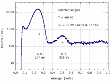
2. Low Energy Performance
As the first production of DEPFET APSs was targeting the principle prove of the device not much emphasis was put in the fabrication of a thin radiation entrance window. Nevertheless, the device is able to detect C-K X-rays (277 eV) with an energy resolution of 90 eV FWHM and a peak/valley ratio of 20 at an operating temperature of -60 °C (fig. 9). For the second generation of DEPFET APSs an optimized thin entrance window technology will be applied which is capable to provide the C-K line with a resolution of 45 eV FWHM.
Fig. 9. Spectrum of C-K (277 eV) and O-K (525 eV) recorded by a DEPFET APS at a temperature of -60 °C. The energy resolution is 90 eV FWHM at 277 eV, the peak/valley ratio is 20.
3. Quantum Efficiency
The quantum efficiency of the DEPFET APS is given by the entrance window properties for low energy X-rays and by the absorption physics of silicon with a given thickness for high energy photons. Figure 10 shows the quantum efficiency obtained with a pnCCD providing values ≥ 90 % in the energy band from 400 eV to 11 keV [25]. As the DEPFET APS uses the same window technology and silicon bulk material the curve is also valid in this case.
Fig. 7. Photograph of an APS hybrid with the 64 x 64 sensor chip in the center, SWITCHERII control chips for readout/reset selection of one pixel row (left and right), and the 64-channel CAMEX readout chip at the bottom.
Fig. 8. Spectrum of a 55Fe source recorded by a DEPFET APS at a temperature of -40 °C. The energy resolution is 133 eV FWHM at 5.9 keV, corresponding to an equivalent noise charge of 6.6 el. r.m.s.
For the XEUS/XRO WFI it is an option to sacrifice part of the high quantum efficiency at the low energy end by direct deposition of a thin aluminum layer on the entrance window.
The Al layer is then acting both as entrance window stabilizer and as a blocking filter for optical wavelength photons. An Al thickness of 100 nm in combination with a system of thin dielectric layers would suppress the contamination by visible light by a factor > 106, and by UV-photons by a factor of 100, while the quantum efficiency at the C- and O-K-lines would be reduced to 40 % and 70 % (fig. 10). The integration of the blocking filter with the detector as mechanical support would avoid the necessity of developing large-area, freestanding filters.
4. Homogeneity and Yield
The devices of the first prototype generation are very homogeneous. Measured offset values within a 64 x 64 sensor have a variation of 2 % referred to a 5.9 keV signal, variations of the gain and noise at operating temperatures below -20 °C are 5 % and 10 %, respectively. The yield is close to 100 %. In 30 mounted devices with a total of more than 100.000 pixels only two dead pixels have been identified.
5. Radiation Hardness
As DEPFET APSs are also under study as inner vertex detectors of the International Linear Collider (ILC) their radiation tolerance has been demonstrated [26]. Single pixel samples have been irradiated in two setups that use 60Co and a high flux X-ray tube with Mo-target (17.4 keV) as irradiation sources. In both cases the total accumulated dose was close to 1 Mrad. Part of the irradiated DEPFETs was turned on, i.e. a transistor current was flowing during irradiation, and part of the devices was turned off, which is the relevant case for usual APS operation. The observed effects are a shift of the DEPFET gate's threshold voltage by 4 V to 5 V, which can be balanced by supply voltage adjustment, and a tolerable increase of noise from 2.2 el. to 3.5 el. ENC. Compared to the irradiation levels obtained in this ILC-related experiment the
dose expected during the XEUS/XRO lifetime is significantly lower, i.e. in the order of 10 krad, and radiation hardness is not considered as potential problem of the Wide Field Imager.
6. The Mesh Experiment
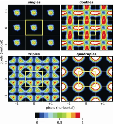
To study the intra-pixel structure of the DEPFET APS the mesh-experiment has been implemented. The pixelated sensor is irradiated through a regular array of pinholes with a diameter considerably smaller than the pixel size. Tilting the pinhole mesh by a small angle with respect to the pixel orientation a repetitive Moiré pattern of hit positions within the pixels is generated. Knowing the mesh dimensions and assuming that all pixels have the identical internal structure the position of the photon absorption can be reconstructed from the pattern with sub-pixel accuracy for each individual X-ray event [27]. That way one image contains the spatially resolved X-ray response of a pixel.
In the experiment the DEPFET APS has been irradiated with Cr-Kα X-rays (5.4 keV) through a gold mesh with a thickness of 10 μm and 5 μm pinholes on a 150 μm orthogonal pitch. The analysis of the mesh data produces the position- dependent probability of a photon to end as a single, double, triple, or quadruple pixel event (fig. 11). The mesh method will be used as experimental access to study the charge collection efficiency as function of pixel topologies and operation parameters.
Fig. 10. Quantum efficiency of a pnCCD [25] (blue) with entrance window technology and thickness equal to a DEPFET APS. Direct deposition of an Al-filter on the entrance reduces the quantum efficiency at the low energy end (red).
Fig. 11. Results of the mesh method applied to a DEPFET APS operated at -60 °C with a back diode voltage of -150 V. The 3 x 3 pixel images show the color-coded position resolved probability of a photon to be detected as single, double, triple or quadruple pixel pattern.
G. Next Steps
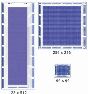
The second generation of DEPFET APSs is currently in production and scheduled to be available in summer 2007.
Apart from minor modifications with the goal of improved charge collection and low-voltage clear the pixel layout remained basically unchanged. The pixel size is again 75 μm x 75 μm.
Based on the high yield of the first DEPFET APS fabrication the formats of the second generation devices will grow substantially to proof that the technology is prepared for the production of large area sensors with a perspective of wafer-scale devices. Next to the previous standard format of 64 x 64 pixels the wafer will include sensor formats of 256 x 256 pixels and 19.2 mm x 19.2 mm sensitive area and 128 x 512 pixels with 9.6 mm x 38.4 mm sensitive area (fig. 12). The 256 x 256 format will be available in two readout versions: single-sided readout, i.e. 256 rows to be read consecutively, and double-sided readout, i.e. two independent halves with 128 rows each and to be read in parallel. The 128 x 512 format is the equivalent one of the 16 sub-segments of the XRO/XEUS Wide Field Imager as shown in fig. 2.
IV. FURTHER DEPFET OPTIONS
A. Macro Pixel Detector
Present missions in X-ray astronomy and planetary research apply imaging spectrometers using X-ray optics with reduced angular resolution. The sensors should still have a good energy resolution but to avoid over-sampling and an unnecessary stream of irrelevant data the pixel size should be in the order of several hundred micrometers. Two examples are the MIXS (Mercury Imaging X-ray Spectrometer) telescope of the
European BepiColombo Mercury mission [28] and the French- Italian X-ray observatory Simbol-X [29], [30], which require pixel sizes of 300 μm and 625 μm on formats of 64 x 64 and 128 x 128.
To combine a large pixel size with a low noise readout element the DEPFET can be integrated in the center of a Silicon Drift Detector (SDD) [31]. In this design the DEPFET is surrounded by a number of concentric drift ring diodes (fig. 13). The drift rings are biased to a step-wise increasing negative potential from the inmost to the outmost ring. The resulting electric field has a strong radial component and drives radiation-generated electrons towards the central readout device. By adjusting the number and the width of the drift rings the pixel dimension is scalable to any value from 50 μm to 1 cm. Based on the SDD/DEPFET cell an active Macro Pixel Detector (MPD) can be formed by matrix arrangement and suitable on-chip wiring. From an operation and readout point of view the MPD is identical to the DEPFET APS described above. The MPD principle has been confirmed by a first generation of prototype devices [32].
The Macro Pixel Detector concept is also an option for the XEUS/XRO Wide Field Imager to adjust the sensor's spatial granularity in case the telescope's angular resolution of the does not meet the specified value of few arcsec.
B. Repetitive Nondestructive Readout
A DEPFET conserves the charge information during the readout. This feature can be exploited for Repetitive NonDestructive Readout (RNDR) realized by putting two single DEPFETs in a pixel, connecting their charge storing region by an additional transfer gate, and a cyclical CCD-like intra-pixel charge transfer between both internal gates (fig. 14) [15], [33]. With every transfer the signal charge can be measured independently. Taking the average value of a large
Fig. 12. Layout plots of the large format DEPFET APSs of the next device generation in comparison to the previous 64 x 64 standard format.
Fig. 13. Layout plot of an SDD/DEPFET Macro Pixel with a pixel size of 500 μm x 500 μm. Five concentric drift rings (shown in red) generate an electric field that drives signal electrons to the DEPFET readout element in the pixel center.
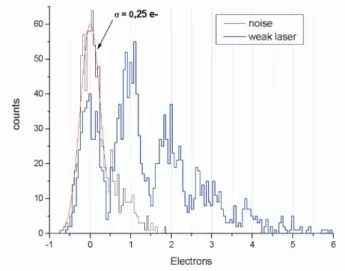
number N of these measurements the serial noise is reduced by N1/2. The repetitive readout of the same information not only reduces the white noise, but also averages out the 1/f noise. As the total readout time is N times longer than the time needed to perform a single readout the device is intended for low-noise and low-flux applications. It has been demonstrated that applying RNDR with N = 360 independent readings in 10 msec reduces the electronic noise from 3.3 el. ENC of a single measurement to 0.25 el. ENC (fig. 15) [33]. This is to our knowledge the best noise value ever obtained with silicon radiation detectors. It allows for measurements on the level of single electron resolution, i.e. one can for example 'count' the number of single optical photons absorbed in the detector.
The implementation of RNDR-capable DEPFETs e.g. in a spatially limited region of the sensor's center is also an option for the XRO/XEUS Wide Field Imager.
V. CONCLUSIONS
A DEPFET based Active Pixel Sensor has been selected for the XEUS/XRO wide field imaging spectrometer as one of two core instruments. A first batch of prototype devices with 64 x 64 pixels and a pixel size of 75 μm x 75 μm has been fabricated and tested. The performance figures are already close to the XEUS/XRO requirements. A second generation of DEPFET APSs with significantly larger formats is in production. A scalable readout and control system is in operation, new versions of readout ASICs with increased speed are in development. The concept of the DEPFET also allows for new devices and operation modes, e.g. Macro Pixel Detectors with adjustable pixel size and Repititive Nondestructive Readout with sub-electron resolution.
REFERENCES
[1] G. Bignami, P. Cargill, B. Schutz, C. Turon on behalf of the Science advisory structure of ESA, and by the Executive of the Science Directorate, supported by Nigel Calder, Cosmic Vision - Space Science for Europe 2015-2025, ESA publication BR-247, 2005, pp. 38-61 [2] M. Bavdaz, D. Lumb, A. Peacock, M. Beijersbergen, S. Kraft,
Development of x-ray optics for the XEUS mission, Proceedings of the SPIE, vol. 5539, no. 1, 2004, pp. 95-103
[3] N. Rando, A. Lyngvi, P. Gondoin, D. Lumb, M. Bavdaz, P. Verhoeve, D. de Wilde, A. Parmar, T. Peacock, ESA study of XEUS, a potential follow-on to XMM-Newton, Proc. ‘6th Internat. Conf. on Space Optics’, ESTEC, Noordwijk, The Netherlands, 27-30 June 2006, ESA Special Publication SP-621, 2006
[4] P. Verhoeve, N. Rando, A. Peacock, D. Martin, R. den Hartog, Superconducting tunnel junctions as photon-counting imaging spectrometers from the optical to the X-ray band, Optical Engineering, vol.41, no.6, 2002, pp. 1170-1184
[5] P.A.J. de Korte, J.J. van Baar, N.H.R. Baars, F.E. Bakker, W.M.B. Tiest, M.P. Bruijn, A. Germeau, H.F.C. Hoevers, M. Kiviranta, E. Krouwer, J. van der Kuur, M.P. Lubbers, W.A. Mels, M.L. Ridder, H. Seppae, R.J. Wiegerink, A cryogenic imaging X-ray spectrometer for XEUS readout by frequency-division SQUID multiplexers, Proceedings of the SPIE, vol.5501, no.1, 2004, pp. 167-176
[6] M.P. Bruijn, M.L. Ridder, E. Krouwer, H.F.C. Hoevers, P.A.J. de Korte, J. van der Kuur, Progress in fabrication of microcalorimeter arrays:
X-ray absorbers and high-density stripline wiring, Nuclear Instruments
& Methods in Physics Research, Section A, vol. 559, no.2, 15 April 2006, pp. 444-446
[7] D. Barret, XTRA: the fast X-ray timing detector on XEUS, AIP Conference Proceedings, no.714, 2004, pp. 405-412
[8] L. Strüder, D. Barret, C. Fiorini, E. Kendziorra, P. Lechner, Fast timing on XEUS, Proceedings of the SPIE, vol. 5165, no.1, 2004, pp. 19-25 [9] C. Budtz-Jorgensen, T. Takahashi, L. Piro, I. Kuvvetli, A. Holland,
D. Lumb, P. de Korte, The XEUS hard X-ray camera, Proceedings of the SPIE, vol.5165, no.1, 2004, pp. 37-44
[10] R. Bellazzini, L. Baldini, A. Brez, E. Costa, L. Latronico, N. Omodei, P. Soffitta, G. Spandre, A photoelectric polarimeter based on a Micropattern Gas Detector for X-ray astronomy, Nuclear Instruments
& Methods in Physics Research, Section A, vol. 510, 2003, pp. 176-184 [11] R. Bellazzini, F. Angelini, L. Baldini, F. Bitti, A. Brez, F. Cavalca,
M. Del Prete, M. Kuss, L. Latronico, N. Omodei, M. Pinchera, M.M. Massai, M. Minuti, M. Razzano, C. Sgro, G. Spandre, A. Tenze, E. Costa, P. Soffitta, Gas pixel detectors for X-ray polarimetry applications, Nuclear Instruments & Methods in Physics Research, Section A, vol. 560, 2006, pp. 425–434
[12] G. Hasinger, M. Arnaud, X. Barcons, D. Barret, J. A. Bleeker, H. Böhringer, A. Comastri, A.C. Fabian, J. S. Kaastra, H. Kunieda, M. Mendez, A.N. Parmar, G.G.C. Palumbo, T. Takahashi, M.J.L. Turner, The new XEUS science case, to be published in Proceedings of the SPIE, vol. 6266, 2006
Fig. 14. Conceptual view of a pair of linear DEPFETs with transfer gate in between for nondestructive repetitive readout [33].
Fig. 15. Low level light spectrum obtained by an RNDR-DEPFET as shown in fig. 14 with 360 consecutive readings at -40 °C. The electronic noise is 0.25 el. ENC and one can clearly separate the signals of zero, one, two, and more electrons. The asymmetric shape of the noise peak (grey) is caused by the accumulation of leakage current during the readout time [33].
[13] A.N. Parmar, M.J.L. Turner and the XEUS Science Definition Team, XEUS Science Requirements Document, ESA Technical Note SA/05.001/AP/cv, March 2006
[14] J. Kemmer and G. Lutz, New semiconductor detector concepts, Nuclear Instruments & Methods in Physics Research, Section A, vol. 253, 1987, pp. 365-377
[15] S. Wölfel, S. Herrmann, P. Lechner, G. Lutz, M. Porro, R. Richter, L. Strüder, J. Treis, Sub-electron noise measurements on repetitive non- destructive readout devices, Nuclear Instruments & Methods in Physics Research, Section A, vol. 566, 2006, pp. 536-539
[16] D. Barret, M. Bavdaz, C. Budtz-Jorgensen, E. Costa, L. Duband, P. de Korte, A. Holland, P. Lechner, D. Lumb, A. Parmar, L. Piro, L. Strüder, T. Takahashi, P. Verhoeve, G. Villa, X-ray Evolving- Universe Spectroscopy - the XEUS instruments, ESA Special Publication SP-1273, 2003
[17] E.R. Fossum, Are CCDs Dinosaurs?, Proceedings of the SPIE, vol. 1900, 1993, pp. 2-14
[18] J. Treis, P. Fischer, O. Haelker, M. Harter, S. Herrmann, R. Kohrs, H. Krüger, P. Lechner, G. Lutz, I. Peric, M. Porro, R.H. Richter, L. Strüder, M. Trimpl, N. Wermes, DEPMOSFET Active Pixel Sensor Prototypes for the XEUS Wide Field Imager, IEEE Transactions on Nuclear Science, vol. 52, No. 4, 2005, pp. 1083-1091
[19] P. Fischer, W. Neeser, M. Trimpl, J. Ulrici, N. Wermes, Readout concepts for DEPFET pixel arrays, Nuclear Instruments and Methods in Physics Research Section A, vol. 512, 2003, pp. 318-325
[20] G. Lutz, W. Buttler, H. Bergmann, P. Holl, B.J. Hosticka, P.F. Manfredi, G. Zimmer, Low noise monolithic CMOS front end electronics, Nuclear Instruments and Methods in Physics Research Section A, vol. 263, 1988, pp. 163-173
[21] L. Bombelli, C. Fiorini, M. Porro, A. Longoni, S. Herrmann, W. Buttler, VELA: the CMOS Circuit Based on Fast Current Read-Out for X-Ray Spectroscopy with DePMOS Pixels, presented at the IEEE Nuclear Science Symposium, talk , San Diego, 31.Oct. 2006
[22] J. Treis, P. Fischer, O. Hälker, M. Harter, S. Herrmann, R. Kohrs, H. Krueger, P. Lechner, G. Lutz, I. Peric, M. Porro, R.H. Richter, L. Strüder, M. Trimpl, N. Wermes, First results of DEPFET-based active-pixel-sensor prototypes for the XEUS Wide-Field Imager, Proceedings of the SPIE, vol.5501, no.1, 2004, pp. 89-100
[23] R.H. Richter, L. Andricek, P. Fischer, K. Heinzinger, P. Lechner, G. Lutz, I. Peric, M. Reiche, G. Schaller, M. Schnecke, F. Schopper, H. Soltau, L. Strüder, J. Treis, M. Trimpl, J. Ulrici, N. Wermes, Design and technology of DEPFET pixel sensors for linear collider applications, Nuclear Instruments and Methods in Physics Research Section A, vol. 511, 2003, pp. 250-256
[24] M. Porro, G. Ferrari, P. Fischer, O. Hälker, M. Harter, S. Herrmann, N. Hörnel, R. Kohrs, H. Krueger, P. Lechner, G. Lutz, I. Peric, R.H. Richter, L. Strüder, J. Treis, M. Trimpl, and N. Wermes, Spectroscopic Performance of the DePMOS Detector/Amplifier Device With Respect to Different Filtering Techniques and Operating Conditions, IEEE Transactions on Nuclear Science, vol. 53, No. 1, 2006, pp. 401-408
[25] N. Meidinger, S. Bonerz, J. Englhauser, G. Hasinger, R. Hartmann, S. Herrmann, P. Holl, G. Kettenring, N. Kimmel, G. Lutz, E. Pfeffermann, P. Predehl, H. Soltau, L. Strüder, CCD-detector development for the DUO and the ROSITA missions, Proceedings of the SPIE, vol.5501, no.1, 2004, pp. 66-77
[26] L. Andricek, P. Fischer, K. Heinzinger, S. Herrmann, D. Herz, M. Karagounis, R. Kohrs, H. Krüger, P. Lechner, G. Lutz, H.-G. Moser, I. Peric, L. Reuen, R.H. Richter, C. Sandow, M. Schnecke, F. Schopper, L. Strüder, E. v. Törne, J. Treis, M. Trimpl, J. Velthuis, N. Wermes, S. Wölfel, The MOS-Type DEPFET Pixel Sensor for the ILC Environment, Nuclear Instruments and Methods in Physics Research Section A, vol. 565, 2006, pp. 165-171
[27] H. Tsunemi, K. Yoshita, S. Kitamoto, New technique of the X-ray efficiency measurement of a charge-coupled device with a subpixel resolution, Japanese Journal of Applied Physics, vol. 36, no. 5A, (1997) pp. 2906-2911.
[28] R. Grard, M. Novara, G. Scoon, BepiColombo - A Multidisciplinary Mission to the Hot Planet, ESA Bulletin, vol. 103, 2000, pp. 11-19 [29] P. Ferrando, M. Arnaud, B. Cordier, A. Goldwurm, O. Limousin,
J. Paul, J.L. Sauvageot, P.-O. Petrucci, M. Mouchet, G.F. Bignami, O. Citterio, S. Campana, G. Pareschi, G. Tagliaferri, U.G. Briel,
G. Hasinger, L. Strueder, P. Lechner, E. Kendziorra, M.J.L. Turner, SIMBOL-X: a new-generation hard x-ray telescope, Proceedings of the SPIE, vol. 5168, no. 1, 2004, pp. 65-76
[30] B.P.F. Dirks, P. Ferrando, U. Briel, O. Gevin, E. Kendziorra, P. Laurent, O. Limousin, F. Lugiez, J. Martignac, M. Authier, C. Chapron, P. Lechner, G. Pareschi, Y. Rio, J.P. Roques, P. Salin, L. Strüder, The focal plane of the Simbol-X space mission, to be published in Proceedings of the SPIE, vol. 6276, 2006
[31] P. Lechner, L. Andricek, N. Findeis, D. Hauff, P. Holl, J. Kemmer, P. Klein, G. Lutz, N. Meidinger, E. Pinotti, R. Richter, L. Strüder, C. v. Zanthier, New DEPMOS applications, Nuclear Instruments and Methods in Physics Research Section A, vol. 326, 1993, pp. 284-289 [32] C. Zhang, P. Lechner, G. Lutz, M. Porro, R. Richter, J. Treis, L. Strüder,
S.N. Zhang, Development of DEPFET Macropixel detectors, Nuclear Instruments and Methods in Physics Research Section A, vol. 568, 2006, pp. 207-216
[33] S. Wölfel, S. Herrmann, P. Lechner, G. Lutz, M. Porro, R. Richter, L. Strüder, J. Treis, Sub-Electron Noise Measurements on Repetitive Non-Destructive Readout Devices, presented at the IEEE Nuclear Science Symposium, talk N05-6, San Diego, 30.Oct. 2006