Progress towards a large area, thin DEPFET detector module 2
P. Fischer,
a,1L. Andricek,
cS. Herrmann,
cM. Karagounis,
bR. Kohrs,
bC. Kreidl,
aH. Kr¨uger,
bG. Lutz,
cH. G. Moser,
cI. Peri´c,
aM. Porro,
cL. Reuen,
bR. H. Richter,
cS. Rummel,
cC. Sandow,
bL. Str¨uder,
cE. v. T¨orne,
bJ. Treis,
cM. Trimpl,
bJ. J. Velthuis,
bN. Wermes
baUniversity of Mannheim, B6, 26, D-68161, Mannheim, Germany
bUniversity of Bonn, Physikalisches Institut, Nussallee 12, D-53115, Bonn, Germany
cMax Planck Institute Semiconductor Laboratory, Otto-Hahn-Ring 6, D-81739, M¨unchen, Germany
Abstract
Large arrays of depleted field effect transistor (DEPFET) detector elements are one possible technology for the vertex detector of the planned International Linear Collider. The main challenges are the production of large (10 cm
2) devices with an average thickness of around 100
µm (silicon) and their fast column parallel readout. Thispaper describes in some detail how a DEPFET based sensor module could be built and presents the design of the latest generation of ‘Switcher’ steering chips.
Key words: particle sensor, vertex detector, DEPFET, readout electronics, International Linear Collider
1. Introduction
The main requirements for the vertex detector at the planned International Linear Collider (ILC) are
– a radiation length one order of magnitude below that of the vertex layers at LHC, i.e. in the order of 0.1% (≈ 100 µm of silicon) per layer,
– a high spatial resolution of a few micrometers,
1 Corresponding author. Tel.: +49-621-181-2735, fax:
+49-621-181-2734. E-mail address: peter.fischer@ti.uni- mannheim.de
2 Work supported by the German Ministerium f¨ur Bil- dung, Wissenschaft, Forschung und Technologie (BMBF) under contract no. 05HS4VM1/5
– a readout adapted to the time structure of ILC (5 bunch trains per second with 2820 bunches within 950 µs),
– a high granularity and readout speed to cope with the expected high hit densities of up to 0.15 hits per mm
2per bunch crossing in the inner- most layer (including a safety factor 3)[1] and – a radiation tolerance of 360 krad per year[1].
Several technologies like Charge Coupled Devices
(CCDs), In-situ Storage Image Sensors (ISIS) [2,3],
Active Pixel Sensors [4,5] and depleted field effect
transistors (DEPFETs) are presently being opti-
mized for a possible application in the ILC vertex
detector. This paper presents ongoing work on
DEPFET matrices with a focus on a possible mod-
ule geometry and a description of new gate/clear
steering electronics. The following section de- scribes some properties of existing DEPFET de- vices. Section 3 presents in some detail a possible module geometry, followed by a description of the new Switcher steering chips in section 4.
2. DEPFET Single Device and Matrix Operation
The depleted field effect transistor [6] is a de- vice with built in amplification: The electrostatic field in a fully sideward depleted silicon structure is shaped such that all electrons generated by ion- izing particles, Xrays or photons are collected in a small volume which is located under the channel of an integrated p-channel field effect transistor.
Both, JFETs and MOSFETs, can be used. The negative charge in this ‘internal gate’ leads to a in- crease of the channel current according to the small signal charge gain g
q≈ 0.5 . . . 1 nA per electron.
The current can be completely switched off with an additional, ‘external’ gate. Charge collection is fully efficient also while the device is switched off, so that a low power operation is possible. The ac- cumulated charge can be measured as a voltage change at the source in ‘source follower’ readout, or as a current signal at the drain in ‘drain read- out’ . The drain voltage can be kept at a constant potential with suited readout electronics for the latter case, so that a fast readout is possible even with high bus capacitances [7].
The charge accumulated in the internal gate can be removed through a clear contact with a posi- tive voltage pulse. In the operation mode used for ILC, a complete clear is mandatory to avoid noise contribution by varying remaining charges. By ap- propriate implantations in the device it has been possible recently to lower the required clear voltage step to ≈ 7 V
3. It is still a challenge, however, to construct radiation tolerant low power electronics able to generate such voltage steps which should be as short as 20 ns for a total capacitance of sev- eral 10 pF.
3 Present devices use an additional ‘clear gate’ held at a constant potential to simplify clearing at low voltages.
This feature is not further described in this paper.
Two dimensional arrays are constructed by con- necting gates and clears in rows and the drains in columns, holding all sources at a common po- tential. After a charge accumulation period, a row is turned on by pulling its external gate line low.
The current in all drain columns is measured and compared to the current with empty internal gate, which is obtained by pulsing the clear line. This sequence is repeated periodically for all rows. In order to cope with the high occupancy at the in- nermost ILC layer, several readout frames must be taken during one ILC burst. This imposes a row readout rate of 10 MHz or more. At these fre- quencies, readout noise will be dominated by ther- mal noise of the electronics and not by the intrin- sic noise of DEPFET devices, which can be be- low 2 electrons (enc) at room temperature for slow shaping times of 10 µs. Several small matrices with 64 × 128 pixels have been operated successfully with fully integrated gate/clear steering and drain readout electronics. As an example, a signal/noise ratio of ≈ 110 has been obtained for minimum ion- izing particles in a test beam using 450 µm thick sensors.
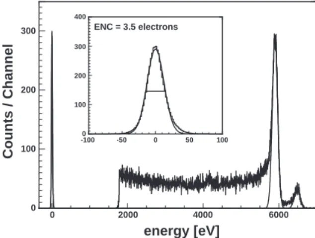
energy [eV]
ENC = 3.5 electrons
100
100
0 50
-50
-100 100
200 300 400
0
0 0 2000 4000 6000
200 300
Counts / Channel
Fig. 1.55F espectrum obtained with an irradiated single DEPFET device (see text).
Due to the high collecting field in the device,
no severe degradation of the ‘internal’ DEPFET
is expected after radiation. The external gate suf-
fers from threshold shift, however. Several consis-
tent irradiations have shown that these shifts are
in the order of −5 V after nearly 1 Mrad. They can
be compensated for by adjusting the gate voltages
until the initial drain current is reached. Only a small (< 10%) decrease in charge gain g
qhas been observed. The noise of the devices is still excellent after irradiation, as illustrated in fig. 1, where a
55
F e spectrum is measured with a DEPFET that has been irradiated to 912 krad (
60Co). The mea- surement has been obtained at room temperature with a shaping time of 10 µs at a DEPFET bias current of only 40 µA. The noise determined from the pedestal peak of 3.5 electrons must be com- pared to the value of 1.6 electrons measured with the same device before irradiation.
3. DEPFET Module Description
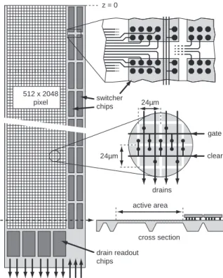
A possible geometry for a DEPFET vertex de- tector half-module is depicted in fig. 2. The num- bers given in the following are realistic estimations, based on existing devices. They may be optimized with maturing sensor and chip designs and based on more realistic simulations of sensor and physics performance within the ILC detector. The active area of 12.3 × 98.3 mm
2consists of 512 × 4096 DEPFET pixels of 24 × 24 µm
2size (Fig. 2 shows half a module). This major part of the module is thinned to ≈ 50 µm with, possibly, some inte- grated support bars for mechanical stability. The 300 µm thick support frame at the left side is only half a millimeter wide to facilitate the assembly of a barrel with nearly 100% track coverage. Adja- cent pixels in two consecutive rows are grouped in pairs, respectively, sharing one horizontal clear and gate signal (see detail in fig. 2). The matrix there- fore effectively consists of 2048 double rows with a pitch of 48 µm. Each pixel pair has two indepen- dent drain connections, so that 1024 drain readout channels with a very fine pitch of only 12 µm are required on both ends of the module.
The frame on the right side supports 2 × 16 Switcher steering chips with 128 channels each to control the gate- and clear signals. The width of this extension must be minimized as much as pos- sible as it is located in the active area. Structured thinning of the extension may be mechanically pos- sible. The present Switcher3 chips have a width of 1.42 mm so that two chips with a small gap and
z = 0
512 x 2048 pixel
24µm switcher 24µm chips
active area
cross section drains
gate
clear
drain readout chips
Fig. 2. Possible geometry of one half of a ILC DEPFET module (dimensions are not to scale).
some free space at the sides can be accommodated
within 3.5 mm. The Chips will be thinned down to
50 − 100 µm to reduce radiation length. The con-
nection to the sensor will be achieved with single
chip gold stud bumping, to begin with. Our present
technology uses a 17.5 µm diameter wire to obtain
gold spheres with a free air ball diameter of below
50 µm. The studs are placed on 60 − 80 µm diam-
eter pads on both, chip and sensor, sides. Flipping
is performed on a manual machine with or without
anisotropic epoxy glue. The additional radiation
length introduced by these gold bump connections
corresponds to an increase in average silicon thick-
ness of the active area of ≈ 15 µm. This value can
be reduced efficiently by going to slightly smaller
ball diameters. The power supply and steering sig-
nals for the switchers are routed on the thick frame
using the two available aluminum layers. The ex-
pected power dissipation of the final switcher chips
will be very low, as only one row must be steered
at a time. No special cooling should therefore be
required in the active area.
The current signals from the 1024 drain lines will be processed by special readout chips located at the bottom and at the top of the module. Due to the narrow channel pitch of 12 µm, bump bonding seems mandatory here as well. A successor of the Curo chip [10] with many improvements and mod- ifications and a suited pad geometry is presently under development. This chip will be the dominant source of power dissipation. Due to the location outside of the acceptance, bringing out the gener- ated heat and the huge amount of data should be feasible.
The arrangement of steering chips along the long edge of the module simplifies cooling and signal routing. The frame rate, however, is limited due to the large number of rows (2048 pixel rows or 1024 double rows per side). At a double row read- out time of 50 ns, for instance, a full frame requires
≈ 50 µs, so that 20 frames can be read within one ILC burst. Placing the drain readout chips at the long edge could speed this up by a factor of four at the expense of an increased heat dissipation in the active volume. More detailed studies of the hit background and the determination of realistic oc- cupancy limits are required to chose among various possible scenarios.
3.1. Progress in Thinning Technology
One key element for the successful construc- tion of a DEPFET vertex detector module is the technology for achieving thin active areas with a monolithic thicker silicon support structure. As described in [8], a backside-implanted, oxidized detector grade sensor wafer is first bonded to a mechanical handling wafer. This sandwich is then thinned down until the sensor wafer has reached the desired thickness. 50 µm are obtained rou- tinely. These two processing steps have been car- ried out in research labs for our first test. Recently, the transfer to industrial suppliers using 150 mm wafers has been successfully demonstrated for the production of various diode test structures and full size mechanical samples. A cross section of a thinned sandwich is shown in fig. 3. The sand- wich must then be processed in the facilities of the Semiconductor Laboratory in Munich. While
first test structures had been produced in a test laboratory, the recent production has been carried out in the main lab, where DEPFET processing is possible. After device processing, the backside of the handling wafer is patterned and the major part of the handling wafer is etched away, so that only the thin sensor wafer is left over in the active area.
50 µm
Handing Wafer
1-2 mm
Fig. 3. Cross section of the edge of a handling wafer with bonded sensor wafer, thinned to 50µm thickness.
One crucial question has been weather the qual- ity of the devices is degraded by this slightly more complicated processing sequence and by the etch- ing step. Various large area (10mm
2) diodes have therefore been produced and the CV- and IV char- acteristics have been evaluated. Full depletion is reached at 50 V as expected for 50 µm thin devices on a substrate with a resistivity of 150Ω cm. The leakage currents of typically 100 pA/ cm
2(at 50 V) are excellent values. Only ≈ 10% of the devices have leakage currents increased by a factor of five.
No significant difference in behavior between nor- mal and thin diodes has been observed.
4. The Switcher3 Gate/Clear Steering Chip In the existing test setups, the control of the gate and clear signals is achieved with the Switcher2 steering chip. This chip has been designed 2002 in a 0.8 µm high voltage technology in order to be able to deliver voltage steps of up to 30 V for test purposes. This chip is not suited for ILC, however, for several reasons (geometry, power dissipation, speed, insufficient radiation hardness). A new chip, Switcher3, has therefore been designed with the following main goals:
– Geometry suited for module construction (slim
and long). Two dimensional arrangement of
bump bonding pads. 128 channels.
– Voltage steps of up to 10 V, sufficient for opera- tion of the latest DEPFET devices.
– Minimal dynamic power dissipation, close to zero static power dissipation.
– Settling time of ≈ 20 ns for a 9 V step and a load capacitance of 20 pF.
– Radiation tolerance of at least 1 Mrad.
– Flexible sequencer allowing multiple readout of regions of interest.
– Minimum number of supply, bias and control sig- nals to simplify wiring on the sensor frame.
9V 9V
9V
6V
3V 0V 3V 6V 6V 6V 6V
6V
6V
x x+3V
0V 9V 3V
0V 6V
3V
0V
0V 3V 3V 3V 3V 6V 9V
9V
out
0V 6V
9V 9V
0V 0V
6V 6V 9V
3V
3V
0V in
3V
0V 3V
a b c
SRAM
SRAM
0V 9V
9V
0V 0V
in SRAM
9V
Fig. 4. Simplified schematic of the ‘high voltage’ switch.
The operation points for a supply of 9 V are shown for high output (a) and low output (b). The required gate voltages are generated by ac-coupled SRAM cells.
4.1. HV Switch
One of the biggest challenges for this new chip was the design of a radiation tolerant analog switch able to operate at up to 10 V. Irradiations of Switcher2 chips had shown, that the used HV- devices with thick gate oxides severely degrade after small (< 50 krad) doses already, as expected.
Thin gate devices, on the other hand, do not withstand the required voltage. The adopted so- lution is illustrated in fig. 4: Three stacked 3.3 V NMOS/PMOS devices are used to pull the output to ground or to the positive switch voltage, respec- tively (similar to a circuit in [9]). The transistors are operated such that under no circumstances
the voltage differences at the terminals exceed the allowed limit. Fig. 4 (a) and (b) show the required voltages for high or low output, respectively, for an illustrating supply voltage of 9 V. The gate voltages of the middle NMOS (PMOS) can always be held at 3 V (6 V), while the other gates must be switched between 0 V/3 V, 6 V/3 V and 6 V/9 V.
The required level-shifting is achieved with SRAM cells which are operated with the corresponding supply voltages and which are flipped by capaci- tive coupling of a 3 V step signal onto the internal storage node. The feedback inverters in the SRAM cells are current limited so that flipping is simpli- fied and capacitors of ≈ 200 fF are sufficient. A reset/set signal in the SRAM cells can be used to define the initial polarity. This level shifting has no dc current consumption, as required.
Note that the stacked arrangement of MOS de- vices requires separate well connections for both, NMOS and PMOS devices. The well diodes must be able to tolerate a reverse bias of up to 9 V. For these reasons, the AMS 0.35 µm high voltage tech- nology, which offers many combinations of wells, has been used.
A first prototype of this switch has been fab- ricated. The switching speed is as required. No degradation of the switch has been observed dur- ing a first X-ray irradiation of up to 600 krad.
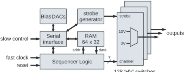
outputs
Sequencer Logic RAM 64 x 32 Serial
interface
Bias DACs strobe
generator strobe
channel 10V
0V
128 ‘HV’ switches slow control
fast clock reset
addr data
7
Fig. 5. Block diagram of the Switcher3 steering chip.
4.2. Block Diagram
The 128 switches are controlled by a simple, but
flexible sequencer, which represents the heart of
the steering logic. The sequencer RAM (see fig. 5)
containing 64 instruction words can be written and
read through a serial interface. Every word con-
tains flow instructions (jump, loop, . . . ), load in-
structions for up to 8 loop counters and a com- mand to modify the active channel address. Only two instruction words are required, for instance, to step linearly through all channels. An interrupt in- put allows for fast switching between different se- quencer programs. The global logic also contains a programmable strobe generator for fine tuning of the switch edges with respect to the clock and some bias DACs for the current starving in the SRAM cells and some additional currents in the switch.
A test output can send some internal signals to a monitoring bus. The clock signal uses LVDS levels.
The complete layout has been implemented us- ing rules for radiation tolerant design, i.e. enclosed devices and guard rings where required [11].
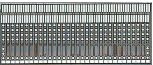
Fig. 6. Photograph of the Switcher3.1 chip. The central part with the bump bond pads has a size of 5.8×1.24 mm2. The wire bond pads at the bottom and at the top are for testing and will be dropped in the following iterations.
4.3. Chip Geometry
A micro photograph of the fabricated chip is shown in fig. 6. The central part consists of 4 rows of 32 bump pads with an opening of 80 µm in a pitch of 180 µm for the 128 outputs. The switches, the SRAM cells and the coupling capacitors are lo- cated in this area. The 32 bump bond pads in the lower row are used for supply, steering and moni- toring. The size of this part is 5.8 ×1.24 mm
2. The additional wire bond pads at the bottom and the top are for initial testing and will be dropped in future chip versions. Several input/output signals have multiple pads for redundancy and some pre- liminary test pads are still used. The final design will require ≈ 15 signals in total. The global cir- cuitry (sequencer, RAM, interface, DACs, strobe generator) is located in the center.
5. Summary and Outlook
Several milestones on the way to a ILC compat- ible DEPFET vertex module have been met in the past year:
– The key properties of the DEPFET devices like pixel size, charge gain, noise, radiation tolerance and minimum clear voltage for fast and com- plete clear are sufficient for ILC matrix opera- tion. Further improvements are likely.
– Further irradiations of single DEPFETs have confirmed the moderate threshold shifts. The slight noise increase of irradiated devices is neg- ligible compared to white noise contributions at the anticipated fast readout speeds. Preliminary irradiations of Switcher3 test structures show no degradation of the ‘high voltage’ part after 600 krad.
– A DEPFET production run with large matrices with either full ILC width or half ILC length (i.e. the full length for one drain readout chip) and many DEPFET test structures has been launched.
– The technology required for manufacturing DEPFETs on thin silicon with an integrated support frame has been prototyped in the main facility of the Semiconductor Lab in Munich on 150 mm wafers using industrial subcontractors for wafer bonding.
– New switcher3 chips have been designed and fab- ricated. They comply to the requirements of ILC (size, bump bonding, speed, radiation tolerance, few pins, . . . ).
– An in-house gold stud bump bonding facility has been set up.
– Several test beam periods have produced suffi- cient data for detailed device studies.
– A simulation framework for optimization of de- tector geometry, pattern reconstruction etc. has been set up.
Some of the next challenges to be addressed are:
– Design of a significantly improved drain readout chip (increased speed, lower noise, shut down possibility,. . . ).
– Characterization of chips and new DEPFET de- vices.
– Assembly of small matrices together with the
next generation readout electronics.
– Further irradiations of Single DEPFETs, Matri- ces, Chips and Modules.
– Detailed analysis of the existing test beam data.
References
[1] The LDC group: Detector Outline Document for the Large Detector Concept,
http://www.ilcldc.org/documents/dod
[2] S. Worm: Recent results on new CCD vertex detectors, Presentation at the Vertex 2006 conference, Perugia, 25- 29 September 2006. To be published in these proceedings.
[3] C. J. S. Damerell: CCD-based vertex detectors, Nucl.
Inst. Meth.A541(2005) pp. 178–188
[4] G. Varner et. al.: Development of a super B-factory monolithic active pixel detector - the Continuous Acquisition Pixel (CAP) prototypes, Nucl. Inst. Meth.
541(2005) pp. 166–171
[5] G. Deptuch, A. Besson, G. Claus, C. Colledani, M. Deveaux, W. Dulinski, A. Gay, G. Gaycken, Y. Gornushkin, D. Grandjean, A. Himmi, Ch. Hu, I. Valin and M. Winter: Monolithic active pixel sensors adapted to future vertex detector requirements, Nucl.
Inst. Meth.A535(2004) pp. 366–369
[6] J. Kemmer and G. Lutz: New Semiconductor Detector Concepts, Nucl. Inst. Meth.A253(1987) pp. 365–377 [7] P. Fischer, W. Neeser, M. Trimpl, J. Ulrici and
N. Wermes: Readout Concepts for DEPFET Pixel Arrays, Nucl. Inst. Meth.A512(2003) pp. 318–325 [8] L. Andricek, G. Lutz, M. Reiche and R. H. Richter:
Processing of Untra-Thin Silicon Sensors for Future e+e−Linear Collider Experiments, IEEE Trans. on Nucl.
ScienceVol. 51, No. 3(June 2004) pp. 1117–1120 [9] B. Serneels, T. Piessens, M. Steyaert and W. Dehaene:
A High-Voltage Output Driver in a 2.5 V 0.25µm CMOS Technology, IEEE J. of Solid State CircuitsVol. 40, No.
3(March 2005) pp. 576–583
[10] M. Trimpl, L. Andricek, P. Fischer, G. Lutz, R. H. Richter, L. Str¨uder, J. Ulrici and N. Wermes: A Fast Readout Using Switched Current Techniques for a DEPFET-Pixel Vertex Detector at Tesla, Nucl. Inst.
Meth.A511(2003) pp. 257–264
[11] W. Snoeys et al.: Layout techniques to enhance the radiation tolerance of standard CMOS technologies demonstrated on a pixel detector readout chip, Nucl.
Inst. Meth.A439(2000) pp. 349–360