Pixel Detector
– Characterization by ADC Transfer Curves
Jakob Haidl
Belle II Pixeldetektor
– Charakterisierung mittels AD-Transferkurven
Jakob Haidl
Pixel Detector
– Characterization by ADC Transfer Curves
Jakob Haidl
Masterarbeit
an der Fakult¨ at f¨ ur Physik
der Ludwig–Maximilians–Universit¨ at M¨ unchen
und am
Max-Planck Institut f¨ ur Physik M¨ unchen
vorgelegt von Jakob Moritz Haidl
aus M¨ unchen
The Super-KEKB accelerator at the KEK high energy research center in Tsukuba, Japan will provide a 40 times higher luminosity. To cope with this high lumino- sity the Belle detector is improved to Belle II, which includes the integration of a two layer DEPFET Pixel Detector (PXD) resulting in a higher vertex resolution. The task of the read-out electronics is to process the high data rate of the PXD. To fulfill these requirements, three different types of ASICs were designed. The foremost of them called Drain Current Digitizer (DCD) converts the drain currents of the DE- PFET pixel sensors into digital code. Since the PXD will be equipped with 160 DCDs, automatic testing of the chips is needed. Analog to digital transfer curves are an appropriate tool for error recognition and optimization of the digitization process within the DCD. A detailed description of different defect types and their origins will be presented. Particular attention is paid to the missing code error, which ari- ses from a transistor mismatch in the DCD, as it is still a prototype version. On this basis an optimization routine is developed, which compensates defects by an adjustment of settings. In an exemplary optimization, the number of channels con- taining missing codes is reduced to 6.25 %, at a combined defect number of 8.2 %.
Finally, a fast routine speeding up the characterization time by a factor of∼90 is propo- sed.
Der Ausbau des Teilchenbeschleunigers SuperKEKB am japanischen Institut für Hoch- energiephysik KEK soll die Erforschung neuer Physik ermöglichen. Dazu wird seine Luminosität um den Faktor 40 erhöht. Gleichzeitig wird auch der neue Belle II Detek- tor mit einem hochauflösenden, zentralen DEPFET-Pixeldetektor ausgerüstet um eine genauere Track- und Vertexauflösung zu erreichen. Der Detektor wird eine enorme Datenmenge produzieren, die nur von eigens dafür entwickelten Auslesechips ver- arbeitet werden kann. Als Erster digitalisiert der sogenannte DCD die Signalströme der Pixelsensoren. Da es sich noch um einen Prototypen handelt, treten Umwand- lungsfehler auf. Um den besten Arbeitspunkt aller verbauten 160 DCDs zu finden, wird ein automatisiertes Testverfahren erstellt. Die verschiedene Parameter, Span- nungen und Ströme, die die Funktionsweise des DCDs steuern, werden mit Hilfe von Transferkurven überprüft. Dadurch können die unterschiedlichen Fehlertypen nach Klassen geordnet und auf ihre Ursprünge zurückgeführt werden. Anschließend wird anhand eines Beispiels gezeigt, wie die Anzahl der fehlerhaften Analog-Digital- Wandler innerhalb eines DCDs auf ein Minimum reduziert werden kann. Das Op- timierungsverfahren bedient sich dabei verschiedener Teststromquellen, wodurch der Gesamtanteil an Umwandlungsfehlern auf 8.2 % gesenkt wird. Ein besonderes Augenmerk liegt dabei auf den sogenannten Missing Codes, die als Lücken in den Transferkurven auftreten und deren Anteil auf 6.25 % reduziert wird. Schlussendlich wird ein verbessertes Verfahren präsentiert, bei dem die benötigte Messdauer auf 1/90 verringert werden kann. Die gezeigten Methoden haben sich als zuverlässig erwiesen und stellen ein geeignetes Mittel zur Optimierung der AD-Wandler des DCDs dar.
1 Introduction 1
1.1 The Belle II Experiment at Super-KEKB . . . 2
1.2 The Belle II Detector . . . 5
1.3 Overview of the Presented Work . . . 6
2 The Pixel Detector of Belle II 7
2.1 The DEPFET Sensor . . . 72.2 A Half-Ladder Module . . . 10
2.3 ASICs . . . 11
2.4 The Pixel Detector . . . 12
3 The Drain Current Digitizer 13
3.1 The Pipeline ADC . . . 153.1.1 Conversion Principle . . . 16
3.1.2 Digital Control Sequence . . . 18
3.1.3 The Current Memory Cell . . . 19
3.1.4 The Comparator . . . 25
3.2 The Analog Channel of the DCD . . . 26
3.2.1 Offset Compensation . . . 26
3.2.2 The Current Receiver . . . 28
3.2.3 Calibration and Configuration . . . 29
3.3 The Digital Block of the DCD . . . 30
3.3.1 Data Conversion . . . 30
3.3.2 Data Transmission . . . 31
4 The Test Setup 33
4.1 Test Modules . . . 34
4.1.1 The EMCM Board . . . 34
4.1.2 The PXD9 Pilot Module . . . 34
4.2 Data Transmission . . . 35
4.2.1 DCD – DHP Communication . . . 35
4.2.2 DHP – DHE Communication . . . 36
4.3 Test Sources . . . 36
4.3.1 The Internal Current Source of the DCD . . . 37
4.3.2 The External Current Source of the DHE . . . 37
4.3.3 DEPFETs as Current Source . . . 39
5 Transfer Curves for ADC Characterization 41
5.1 Properties of the ADC Transfer Curves . . . 435.2 Analog Defects . . . 46
5.2.1 Limited Range & Gain Deviations . . . 46
5.2.2 High Noise . . . 49
5.2.3 Nonlinearity . . . 50
5.2.4 Missing Codes . . . 53
5.3 Digital Defects . . . 60
5.3.1 Communication Errors . . . 60
5.3.2 Single Outliers . . . 62
6 ADC Optimization 67
6.1 Establishing a Data Connection . . . 676.1.1 DHP Delays . . . 67
6.1.2 High Speed Link . . . 70
6.2 Full Optimization of a Module . . . 71
6.2.1 One-Dimensional Sweeps . . . 71
6.2.2 Two-Dimensional Sweeps . . . 74
6.2.3 Supply Voltages . . . 77
6.2.4 Complete Set of Channels . . . 79
6.3 Relation to Physics . . . 82
6.3.1 Calibration . . . 82
6.3.2 Results . . . 83 6.4 Fast Optimization with the DEPFET Current Source . . . 84
7 Conclusion 87
List of Abbreviations 91
Bibliography 93
List of Figures 97
List of Tables 99
The mathematical sciences particularly exhibit order, symmetry, and limitation. These are the greatest forms of beauty. – This statement from Aristotle from around 350 BC survived a very long time as a fundamental hypothesis of natural science. All the more aston- ishing was the detection of the violation of combined Charge Parity (CP) symmetry by Cronin and Fitch in a kaon decay system in 1964 [1]. It took several years until Kobayashi and Maskawa proposed a new scheme of weak interaction explaining the discovery in 1972. Their theory predicted a third family of quarks at a time where neither the bottom nor the top quark were experimentally discovered [2]. CP violation and the flavor mixing due to charge-current interaction were finally integrated into the Standard Model (SM) by the Cabibbo–Kobayashi–Maskawa (CKM) formalism.
CKM predicted the highest significance of CP Violation for a B-meson system, which was confirmed with remarkable consistency by the two independent experiments BaBar at SLAC in California and Belle at KEK in Japan, awarding Kobayashi and Maskawa the Nobel price in 2008 [3]. Despite the great success of the Standard Model in describing matter and its behavior, still some fundamental questions remain unan- swered.
In 1967 Sakharov identified CP violation as the source of the domination of matter over antimatter in the universe [4]. Nevertheless, the Kobayashi–Maskawa model, which is the only source of CP violation in the Standard Model, cannot explain the magnitude of the observed Baryon asymmetry [5]. Unknown sources must exist some- where.
To reveal further secrets of nature, several enormous particle accelerators have been built over the past decades. Some, like the Large Hardron Collider at CERN operating at a center-of-mass energy of up to 14 TeV, are searching for new physics at high energies. Others are attacking the Standard Model with high statistics at the precision
frontier. A significant upgrade of the Belle experiment at the super flavor factory Super- KEKB in Tsukuba, Japan is expected to further enlighten unknown sources of CP viola- tion beyond the Standard Model [6].
1.1 The Belle II Experiment at Super-KEKB
Like its predecessor, Super-KEKB at the Japanese Research Institute for high energy physics KEK is an asymmetrical electron-positron collider with a circumference of 3 km.
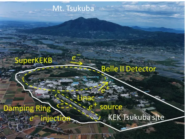
Fig. 1.1 shows a photograph of the entire facility in the Tsukuba plane. Its general goal is the production of boosted B-mesons, which is why it is also known as aB-factory.
The probability for the generation of B-meson pairs is highly increased at the Y(4s) reso- nance with a center-of-mass energy of 10.58 GeV. Since the electrons and positrons are accelerated in two separated rings at different energies of 7 GeV and 4 GeV respectively, the particles get Lorentz-boosted.
In order to prove deviations from the Standard Model, a significant reduction of the measurement inaccuracies compared to former experiments must be achieved. This should be obtained by an increase of the accelerator luminosity as well as an improve- ment of the detector sensitivity.
The luminosity of a storage ring is defined as:
L= f Ne−Ne+
A (1.1)
where f is the bunch collision frequency,Ne−,e+ the number of electrons and positrons in a bunch and Athe bunches’ cross section. By increasingNe−,e+ and particularly, by reducing the beam size with an innovative nano beam scheme, it is planned to reach a peak luminosity ofL=8×1035cm−2s−1, which is 40 times higher than the world record so far held by KEKB. [8]
The luminosity improvement is estimated to not only increase the rate of events by a factor of 50, but as a drawback also the rate of second-order events representing the
Figure 1.1:The Super-KEKB accelerator at KEK in Tsukuba, Japan. Electrons and positrons are injected into two separated storage rings from a low emittance elec- tron/positron gun at a rate of 10 Hz. The Belle II Detector is placed at the interaction point, where bunches collide every 4 ns. [7]
Figure 1.2:An exemplaric decay of two neutral B-mesons. The reconstruction of the decay vertexes is the primary goal of the detector. [9]
background, by a factor of 20 compared to KEKB [8]. This is only one of the challenges the detector has to deal with.
As already mentioned, B-meson decays are used for determining CP violations. A prominent example of such a decay is illustrated in Fig. 1.2. At the interaction point, the collision of an electron and a positron excites the Y(4s) resonance. This state almost im- mediately decays into a pair of neutral B-Mesons. One meson decays into aJ/Ψon the CP side, while the other decays into a D and a charged lepton. The only chance to deter- mine which path one of the B-mesons took is to measure the charge of the lepton on the Tag side [10]. The difference in the decay time∆τindicates the CP violation parameters.
Due to the Lorentz boost the time difference∆τ is transferred into a spatial resolution
∆z. In this way the precise measurement of the decay vertexes is a key to determine CP violation.
Figure 1.3:The Belle II Detector. [12]
1.2 The Belle II Detector
The Belle II Detector is located around the beam pipe at the interaction point. Its main task is the reconstruction of particle trajectories emerging from particle collisions. Like most modern detectors in high energy physics, it is arranged in the typical onion shape formed by different subdetector systems [11]. Fig. 1.3 illustrates the detector struc- ture.
As closest to the beam pipe, the silicon Vertex Detector (VXD) is placed. Consisting of two layers of pixel sensors (PXD) followed by four layers of silicone strip sensors (SVD), it guarantees highest accuracy in particle vertex reconstruction. A combined spatial res- olution of∼20 µm ensures precise identification of trajectory origins, which is not only powerful in measuring CP violation observables but also in discriminating interesting events from the background [8].
The VXD is enclosed by a Central Drift Chamber (CDC), which precisely measures momenta and trajectories of charged particles. Furthermore, it is utilized as a trigger source.
The CDC is surrounded by a Particle Identification System (PID) with the main pur- poses of separating kaons from pions. Electromagnetic calorimeters consisting of
CsI scintillator crystals ensure precise energy measurements. The outermost part of the detector is formed by a system that identifies KL and muons. Moreover, the Belle II detector features further important components, e.g. trigger genera- tor, data acquisition and grid computing. A detailed description can be found in [13].
1.3 Overview of the Presented Work
The main focus of this thesis is the optimization and characterization of the front end readout electronics of the Pixel Detector within the detector environment.
Therefore, Chapter 2 provides a brief overview of the Pixel Detector and the DEPFET sensors it is composed of. Furthermore, its readout and steering chips, so-called ASICs, are introduced. Special attention is paid to the front-end readout chip, called Drain Current Digitizer (DCD) in Chapter 3. This chip converts the signal cur- rents of the DEPFET sensors into digital code. A profound understanding of its conversion principle is needed, as the reduction of conversion errors is the over- all aim of this work. A short overview of the used test setup and test modules is given in Chapter 4. In Chapter 5, the different defect types that can arise dur- ing the digitization process are defined. Chapter 6 then describes the develop- ment of a characterization strategy for the DCD using different test current sources.
The full optimization routine is presented for an exemplary DCD. Thereby, differ- ent setting parameters are probed on their impact on conversion errors. Finally, a fast routine speeding up the characterization time by a factor of ∼90 is intro- duced.
The Belle II Pixel Detector uses DEPFET sensors for high accuracy measurements of the local resolution needed for the reconstruction of decay vertexes. The following section briefly summarizes their working principle.
2.1 The DEPFET Sensor
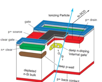
In 1987 Kemmer and Lutz from the Technical University and the Max-Planck Institute for Physics and Astrophysics in Munich proposed a new type of sensor, combining signal detection and amplification within a single transistor [14]. During the following years the technology was developed and further improved by the Semiconductor Lab- oratory of the Max-Planck Society. The sensor is based on a conventional p-channel MOSFET placed on a depleted silicon substrate, which is why it is called Depleted p- channel Field-Effect Transistor (DEPFET). Fig. 2.1 provides a schematic drawing of the sensor.
The n-doped silicon substrate, marked in white, represents the sensitive volume of the sensor. A full depletion of the substrate is reached by means of sideward depletion. A negative voltage is applied to both the source as well as the back contact. As a conse- quence, a layer of potential minimum for electrons is created at the transition of the two depletion volumes. This layer is shifted very close to the top side by applying a much more negative back voltage than source voltage. In addition, a n-doped region is im- planted directly underneath the gate contact, which results in a general potential well for electrons called internal gate.
Figure 2.1:The DEPFET Sensor. Ionizing particles create electron- hole pairs when they traverse the silicon. Due to the applied voltages they drift apart. The electrons accumulate in the internal gate, where they modulate the source drain current. Clear gate and clear voltage are used to empty the internal gate after each readout cycle.
If the sensor is traversed by a particle of sufficient energy, electron hole pairs are cre- ated in the silicon. Due to the sidewards depletion the electrons drift from all over the substrate into the internal gate, whereas the holes are absorbed by the back contact. In a conventional field effect transistor the source-drain currentISDis a function of the gate voltageVG. In the case of the DEPFET, the electrons in the internal gate also create an electrical field effecting a broadening of the conducting channel.Consequently, ISDis the sum of the current evoked by the "external" gate called pedestal currentIpedand the current of the internal gateIsignal.
IDS = Iped+Isignal (2.1)
In this way, it becomes possible to detect traversing particles by means of the electrons in the internal gate. Furthermore, the signal is immediately amplified due to the transis- tor effect. The internal amplification of the DEPFET is defined as:
gq = ∂ISD
∂Qsig VG,VDS
(2.2)
For the expected ranges,gqcan be assumed as constant. It amounts togq ≈400 pA/e− at an external gate voltage of−1 V.
Since the measurement is performed in an indirect way, which is not affecting the number of electrons inside the internal gate, it becomes necessary to remove the charge after each readout cycle. To this end, the DEPFET sensor features additionally positive clear contacts, which are able to empty the internal gate by applying a high positive voltage. In order to prevent a loss of signal electrons during the accumulation phase, the clear contact is shielded by an additional clear gate and a p-doped region inside the substrate. A detailed description of the DEPFET principle can be found in [15] and [16].
The readout of the DEPFET takes place in three iterative steps:
• Sensitive phase: Ionizing particles traversing the DEPFET create electric charge, which accumulates in the internal gate. At the same time, the external gate voltage is set to a positive value leading to a complete pinch-off of the conducting channel.
• Readout phase: The MOSFET is switched on by applying a negative voltage to the external gate. Thus, a conducting channel between drain and source is established. Subsequently, the drain current composed of Iped and Isignal is sampled. For this readout scheme the pedestal current must be known in order to calculate the signal current according to Eq. 2.1. In a dedicated measurement the pedestal current is therefore pre-stored before the readout cycle begins.
• Clear phase: Accumulated electrons are removed from the internal gate by means of a voltage pulse on the clear contact.
In this way the whole readout cycle is controlled via the gate and clear voltage. A sam- pling of the drain current is only required during the readout phase.
Figure 2.2:A half-ladder for the pixel detector. The active area consists of 768·250 DEPFET pixel. Only the active area is thinned to 75 µm, leaving a self supporting structure at the sides. The readout is performed in rolling shutter mode controlled via 14 ASICs. [17]
2.2 A Half-Ladder Module
For the purpose of building a pixel detector, the DEPFET sensors are arranged in arrays of 768·250 pixels, called half-ladders (Fig. 2.2). The excellent signal-to-noise ratio of the DEPFETs allows a thinning of the sensitive area to 75 µm. Since only the sensitive area is thinned, a self supporting frame remains at the sides. The steer- ing and readout of all 192 000 pixel is an enormous challenge. To deal with this, three different types of Application-Specific Integrated Circuits (ASICs) have been de- signed.
2.3 ASICs
The Switcher, which is placed on the long side of the ladder generates the clear and gate voltages for the DEPFETs. The matrix is operated in fourfold rolling shutter mode.
This means that the clear and gate contacts of four pixel rows are connected together.
Such a block is called an electrical row and contains 1000 pixel. The 192 electrical rows are readout subsequently, i.e. only one electrical row is active at a time. Simultaneously, the other 191 rows are in the sensitive phase. This allows for a parallel connection of the drain contacts of each column. Due to the fourfold readout, the number of drain lines has to be quadrupled too. In this way the 768·250 physical pixel can be understood as 192·1000 electrical pixel.
A readout of the full matrix is called a frame and was determined to 20 µs. This leaves ∼104 ns per electrical row for the readout and clear phase. Another ASIC called Drain Current Digitizer (DCD) was designed for sampling and digitizing the drain current during this time period. Since each DCD contains 256 Analog-to-Digital Converter (ADC), four of them are sufficient to process all 1000 drain lines in parallel.
A resolution of eight bit is sufficient to meet the signal-to-noise requirements of the detector. Furthermore, this chip guarantees a constant potential of the drain line capac- itance. The presented thesis is focused on the optimization of the digitization process within the DCD. Thus, a detailed explanation of this chip will be given in the next chap- ter.
The output data of the DCD is transmitted to the Data Handling Processor (DHP).
Its main task is data reduction, since the huge amount of data produced by the DCD would overload the connections to the outside. Therefore, the DHP applies so-called zero-suppression to the data. In a first step the common mode calculated for each elec- trical row is subtracted. Subsequently the pre-stored pedestal values are subtracted for each pixel individually. Only signals being still above a threshold are further transmit- ted via high speed links.
2.4 The Pixel Detector
The Pixel Detector consists of 20 full ladders which approximately form a barrel shape through polyangular arrangement in two layers (see Fig. 2.3). A full ladder is formed by gluing together two half-ladders at their short side. The two layers have a distance to the interaction point of 14 mm and 22 mm and are composed of eight and twelve lad- ders respectively. The outer ladders have a size of roughly 15.4 mm×170 mm and are thus longer than the inner ones with 15.4 mm×136 mm.
Figure 2.3: The Pixel Detector is formed by two layers of sensors in polyangular arrangement. [18]
The main goal of the PXD is to enhance the reconstruction of decay vertexes. Thereby, the reconstruction resolution is depending on a geometrical and a multiple scattering term. With this arrangement, the combined impact parameter resolutionσof the SVD is expected to be≈20 µm.
The PXD features a lot more interesting aspects, whose description would go beyond the scope of this work. The interested reader is referred to [16].
With the development of the DEPFET sensors by J.Kemmer and G.Lutz in 1987 [14], the need for suitable readout electronics converting the signal currents of the pixel matrix into digital data arose. In order to cope with the complexity of this non- standard application, the design of a dedicated chip, so called Application-Specific Integrated Circuits (ASICs), became necessary. In the case of the DEPFET sensors used for the Belle II Pixel Detector (PXD) this chip had to fulfill the following require- ments.
• The main task of the chip is the digitization of the signal currents. A digitization precision of eight bit is sufficient to meet the signal-to-noise requirements.
• Since the PXD is the innermost part of the Belle II detector it is located very close to the interaction point. Therefore the readout chips, which are mounted on the edge of the sensors, will be exposed to high radiation doses. Thus the chip must tolerate an expected radiation dose of at least 70 kGy [19].
• In consideration of the expected high signal background the PXD subdetector requires a sampling rate of 50 MHz [16] in order to enhance the physical perfor- mance of the Belle II detector. Since the matrix is arranged in 192 electrical rows, a sampling period of∼100 ns per ADC must be maintained.
• Furthermore, parallel readout of the 1000 electrical columns of a half ladder is needed. Therefore several chips with a channel number in the order of hundreds are required.
• The drain lines of the matrix have a capacitance of ∼50 pF [19]. The current receiver of the chip must provide a stable potential to ensure fast and precise readout.
• All the mentioned requirements have to be realized on limited space on the edge of the silicon ladder.
It was in the early 2000s when the group of Prof. Peter Fischer from the Institute of Computer Engineering at the University of Heidelberg started working on a readout chip for the DEPFET Sensors. Leading designer Ivan Peri´c’s main idea was to use cur- rent memory cells to memorize and process the signal currents. In this way the whole conversion process is done in current mode. Thus, simplicity is retained, allowing an easier implementation of radiation-tolerant layout techniques, as well as making the use of any pre-converting or pre-amplification unnecessary [19]. The first version of their chip was inspired by the readout chipCUROdesigned by M. Trimpel at the University of Bonn [20]. By improving the current memory cell with a differential transconductor and by implementing this cells as cyclic ADCs, they created the work- ing principle of the cells now used in the PXD. Since then, various enhanced prototypes have been developed [21], but they all share the same conversion procedure. This iterative algorithm is calledredundant signed digitconversion and consists of three basic steps.
1) The input current is sampled and memorized.
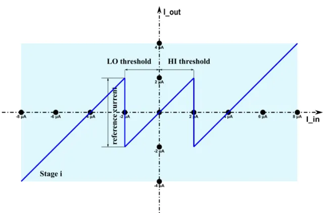
2) The sampled current is compared to two thresholds, one low (LO) and one high (HI). If the signal is lower than the low threshold, the reference current, which is 1/4 of the input range, is added and the output number is set to -1. If the signal is higher than the high threshold, the reference current is subtracted and the output number is set to +1. If the signal is in between the thresholds no current is added or subtracted and the output number is set to 0.
3) The current resulting from 2) is multiplied by two and feed as input to 1).
Subsequently the algorithm starts again from 1). Fig 3.1 shows the transfer characteris- tic of the algorithm, with the input current on the x-axis and the resulting output cur- rent of step 2) on the y-axis. The multiplication of step 3) is not shown.
The redundant signed digit conversion is an iterative algorithm, where every cycle produces one output number ai. The results can be translated to a binary number D:
Figure 3.1:The transfer characteristic of the redundant signed digit conversion
D =
∑
n i=02n−iai (3.1)
In this way,ncycles of the conversion algorithm result in then+1 bit long signed digit D. The right choice of the threshold and reference current is essential for the algorithm to work properly. But before addressing this problem, it is advisable to understand how the conversion procedure is implemented in hardware.
3.1 The Pipeline ADC
The latest Version of the readout chip is called DCDBv4, which is short for Drain Cur- rent Digitizer for Belle version 4. Two different subversions with 256 channels have been manufactured: one with a pipeline ADC and another one with two cyclic ADCs
per channel. In this work only the pipeline version was used and therefore will be re- ferred to as DCD in the following.
3.1.1 Conversion Principle
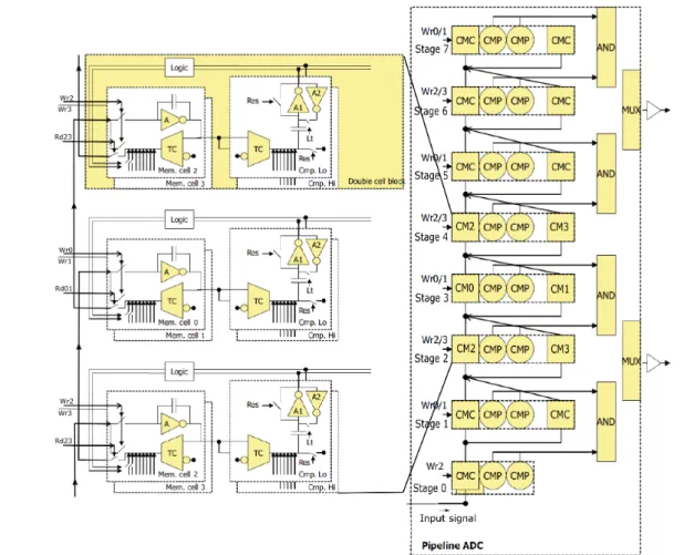
Fig. 3.2 shows the pipeline ADC of one DCD channel. It consists of eight double cell blocks, each containing two comparators and two Current Memory Cells (CMCs).
Inside the double cell blocks both comparators are connected to the first CMC. The left side of the figure shows a detailed view of three of the blocks, where the op- eration cycle is emphasized for stages 2 to 4. The analog-to-digital conversion is performed in four states, which is very similar to the algorithm described above [19].
State 1:
The current from the previous cells (in the case of the first double cell block this is the input signal) is copied to memory cellCM0. The comparators connected to this cell are in reset state, no output is produced.
(Active steering signals: Wr0=1,Rd23=1,Res=1) State 2:
The current from the previous cells is copied to memory cellCM1. Simultane- ously, the two comparators connected toCM0, namelyCmp.LoandCmp.Hi, are switched to active state and compare the current ofCM0to their thresholds.
(Wr1=1,Rd23=1) State 3:
Comparators are now latched and reproduce the conversion results from state 2. Those are used for two purposes. Firstly to control the switchable current sources of CM0and CM1 and secondly to produce the digital output. If the current is higher than the high threshold, the reference current is subtracted and the low and high output bits are set tol=0,h=1. If the current is lower than the low threshold, the reference current is added and the output bits are set to l = 1,h =0. If the current is in between the thresholds no current is added or subtracted,handlare 0. If the reference current and the thresholds are properly
chosen, the sum of the residual currents flowing out ofCM0andCM1fits into CM2. Since all memory cells are of the same type this is equal to multiplication by two.
(Wr2=1,Rd01=1,Lt=1)
State 4:
The currents ofCM0andCM1are copied toCM3. At the same time the compara- tors ofCM2are in compare state.
(Wr3=1,Rd01=1)
Figure 3.2:The pipeline ADC is composed of eight double cell blocks, which contain two current memory cells (CMP) and two comparators (CMP) each. The output bits of two blocks are merged viaANDoperators and multiplexed to two output lines.
On the left side, three of the double cell blocks are shown in detail, including the control signalsWrandRd. Adapted from [22].
From now on states 1 - 4 repeat. With a global clock of 76.23 MHz1 every state takes 26.6 ns. Therefore the total conversion time in eight blocks amounts to 420 ns.
Nevertheless, a new signal can be sampled every 105 ns while the previous sig- nals are still in the pipeline. There is a small difference in the first double cell block. Here, both CMCs sample the input signal simultaneously during state 3, in contrast nothing happens during state 4. Thereby the input range of the ADC is doubled (the current splits up to two cells) and the sampling time is reduced to 26.6 ns.
While the comparators ofCM0in stage 3 produce valid output, the ones ofCM2in the next block are in reset state. Therefore it is possible to merge the data of each two blocks via and-operation (AND). The number of lines transmitting the conversion re- sults to the digital part can be reduced to four (2·2 bit) by additional time multiplexing (MUX).
In this way the conversion produces eight digital output pairs (l0, h0), ...,(l7, h7) per current sample. According to the conversion algorithm as it was described above, h and l correspond to ai = hi−li. Using Eq. 3.1 the signal current can be expressed as discrete signed number ISignal = D128R , with Rbeing the reference cur- rent.
3.1.2 Digital Control Sequence
Each DCD channel has a decoder which generates the digital sequence controlling the ADC. It receives the two bit synchronization signal (Sy0andSy1) as well as the clock signal (bitCk) from the chip’s digital part. Thereof it generatesRd01,Rd23andWr0to Wr3, which steer the respective states of the CMCs. The latch and reset signals of the comparators,LtandRes, are coupled to theWrsignals. Fig. 3.3 shows the temporal se- quence of the control signals.
1 This is the nominal clock frequency of the detector, leading to a sampling rate of 50 MHz. The clock frequency can be reduced to 62.5 MHz in order to guarantee stable testing conditions.
Figure 3.3:The digital control sequence of the pipeline ADC. The sampling periods are marked in red. [22]
3.1.3 The Current Memory Cell
The current memory cell is the fundamental building block of the pipeline ADC. It is an analog-memory element, memorizing and reproducing currents.
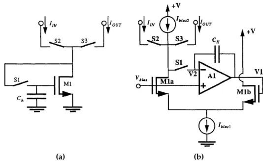
The Basic Cell
The working principle of a current memory cell is best explained by the simplest ver- sion, shown in Fig. 3.4a. It is implemented with a single Metal-Oxide Semiconductor (MOS) transistor, three switches and a hold capacitor.
In the read state switches S1 andS2 are closed. The input current II N flows through S2 into transistor M1. At the same time one part of II N flows through S1, where it loads the hold capacitance Ch and generates a negative feedback at the transis- tors gate. Once the system is in balance and the total current is dumped to ground via M1, the storing process is finished. By opening S1, the gate voltage of M1 is locked in Ch. In the write state only switch S3 is closed and the copied current IOUT flows out of the cell. Notice that the output current has the same sign as the input current. Moreover the current memory cell has the ability to sample and re- produce currents of both signs, which is necessary when writing from one cell to the next.
This basic cell has two drawbacks. Firstly, signal dependent charge injection com- promises the stored voltage ofCh. The charge injection arises during the opening of switchS1. It depends on the signal level, if the source and drain potential ofS1varies with the signal level, as it is the case within the basic cell. In order to achieve high
(a) (b)
Figure 3.4: a) The basic current memory cell. b) The zero voltage switching cell, including amplifierA1and the differential pairM1a&M1b. [23]
precision of the stored voltage, which represents the current sample, both ends ofS1 must be kept at a constant level. Secondly, the memory cells output resistance differs between read and write state. This finite output resistance of M1 limits the sampler’s accuracy when current is transferred from one cell (in read state) to the next (in write state).
The Zero Voltage Switching Cell
The zero voltage switching cell (Fig. 3.4b) introduced by D. Nairn overcomes those drawbacks [23]. Here, amplifier A1 and hold capacitance Ch are used to sample the signal. The more complex differential pair transconductor, implemented in the zero voltage switching cell, works in a similar way as M1 in the basic cell. Again Ch is used as memory element. Out of the stored voltage the amplifier A1 gener- ates a voltageV1 proportional to the input current II N. V1acts on one input of the transconductor (gate of M1b). The other input is fixed (Vbias) as well as the sinks (+V) and the source (Ibias1) of the transconductor. In this way V1 controls which fraction of current from Ibias1flows in the right arm of the transconductor. The rest of Ibias has to flow through M1bin the left arm, where it causes negative feedback
to II N. Once the system is in balance, S1 is used to freeze the voltage across Ch. Afterwards the sampled current is reproduced and transferred to the output via S3.
Notice, that the source Ibias2adds a small amount of current in order to ensure mini- mum speed in the case of small input currents. Therefore it holds IOUT = II N+Ibias2. Contrary to the basic cell, the potential atM1a’sends remains constant in this circuit, due to the negative feedback ofA1. Thereby the circuit shown in Fig. 3.4b provides a solution to both problems of the basic cell. For one thing, the charge injection of S1 becomes mostly signal independent. For another thing, the effective input impedance is reduced significantly by holding the sampler’s input node at constant level. An additional advantage of the constant potential is the admission of the use of P-channel Metal-Oxide Semiconductor (PMOS) transistors only, which tolerate higher radiation doses than N-channel Metal-Oxide Semiconductor (NMOS) transis- tors.
The Pipeline ADC Current Memory Cell
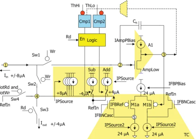
Fig. 3.5 provides a detailed view of the latest version CMC used in the pipeline ADC. The cell basically resembles the zero voltage switching cell, nevertheless some components were adjusted for the use in the pipeline ADC. The main difference is the current adding or subtracting part (Add and Sub) necessary for the analog- to-digital conversion algorithm. The switchable current sources Add and Sub are controlled by the comparators CMP1andCMP2, described in the next section. Be- side this, some smaller changes of implementation details are made. Amplifier A1 is realized as gain stage with the current source IAmpPBias. Its ground is defined by the AmpLowvoltage. The transconductorTCtakes the output voltage of the am- plifier as input on its right side, in the same way as in the zero voltage switching cell. Its sourceIFBPBiasand its sinksIPSource2have a nominal current of 24 µA. The TC’s left input is controlled by fixed but configurable voltage RefFB. The cascodes IFBNCasc are attached to both outputs in order to increase stability of the system.
While the right output is kept at the fixed potentialRefIn, the left side is connected to the cells input and output via node 4. IPsourceCasc adds constantly a current of
8 µA, whileSubandAddadd or subtract a current of 4 µA according to the compari- son result. The input range of the cell is±8 µA while the output range is limited to
±4 µA.
Figure 3.5:A detailed schematic of the current memory cell. The dotted line marks the connection to the comparators Cmp1 & Cmp2 with the logic block controlling the switchable current sourcesAdd&Sub. [22]
The ongoing processes in the CMC might be best understandable by giving an ex- ample. Let’s assume an input current Iin of 5 µA. The system is in the write state (state 1 according to section 3.1.1). Sw1and Sw2 are closed, the logic block is dis- abled and currents ofSub and Add are dumped to RefIn. On its way over node 4, Iin picks up additional 8 µA by IPSource so that a current of 13 µA arrives at node 5. According to Kirchhoff’s circuit laws the sum of currents flowing into the node must be zero. Therefore the current of M1a has to take a value of 11 µA. This leads to 13 µA for M1b. As long as M1b does not fulfill this condition, a part of Iinloads the hold capacitanceCh where it generates negative feedback on the gate of M1b.
Once the system is in balance and the total of Iinflows in node 5, the sampling process is finished. When the system changes to state 2, switches 2 and 3 are opened and the voltage is saved inCh. In this state the output voltage of the amplifier is feed to the comparators via node 3. In the meanwhile the output current is dumped toRefinvia Sw4.
In the read state (state 3 and state 4) the Rdsignal activatesSw3 as well as the logic block. In the example of 5 µA the comparison would result in h = 1, l = 0, lead- ing to a subtraction of 4 µA. Therefore a current Iout of 1 µA would flow out of the cell. Remember that the outputs of both CMCs of a double cell block are summed and feed as input to the next cell block. Thus, the input of the next cell would be 2 µA.
Control parameters
As can be seen in the block diagram, the CMC possesses over a variety of configurable current sources that generate the bias voltages for the CMC. Those are the tuning parameters for optimizing the ADC, which is the aim of this thesis. All this current sources are realized as 7-bit Digital-to-Analog Converter Units (DACs), meaning in a range of 0 to 127, with a full scale of 10 µA. The DACs are globally set for all channels of one DCD and can be accessed via Joint Test Action Group Standard (JTAG). Table 3.1 provides a complete list of the CMC’s configurable current sources with a short descrip- tion.
In order to provide high sampling precision, exact timing of the switching processes is required (e.g. openS1prior toS2). Therefore some of the write and read signals have to be delayed by a few ns. This is done by delay elements controlled byIPDelandIN- Del.
The reference ground signalsAmpLowandRefInare generated by the power supply and feed to the DCD as analog signals.
IAmpPBias The load current source of the amplifier.
IFBNCasc The control voltage of the stability cascodes at the outputs of the transconductor.
IFBPBias Controls the source of the differential pair transconductor
IFBRef The control voltage of the fixed input of the transconductor acting as reference to the second input.
IPSource The control voltage of the switchable cur- rent sourcesAdd&Sub.
IPSource2 Controls the current sinks of the differential pair transconductor.
IpSourceCasc A cascode voltage, improving the stability of theIPSourcecurrent source (not shown in the figure).
IPDel Sets delays for Wr and Rd signals (not shown in the figure).
INDel See IPDel.
Table 3.1:Configurable current sources of the CMC, where Idenotes the current source nature of the DACs,FBstands for feedback transconductor andP&Nrefer to the transistor (PMOS or NMOS) used for converting the current into the control voltage.
3.1.4 The Comparator
Fig. 3.6 shows a schematic drawing of the comparator. The value of the threshold Th, which is 6 µA for a low comparator and 10 µA for a high comparator, is the only difference between them. As already mentioned, both comparators are connected to node 3 of the first CMC of each double cell block. In this way they see the out- put voltage of the CMC’s amplifier. Since the comparators and CMCs use equal transconductors this voltage is converted into equal current. Consequently the output current of the comparator’s transconductor is in the range 0 µA to 16 µA. This current is compared to the threshold. In the case of a low comparator, current below 6 µA results in a negative comparison result Iresult. The same holds for the high compara- tor and currents below 10 µA. In this way the thresholds decide about the sign of
Iresult.
The output stage of the comparator is a latch-like structure, implemented with two cross coupled amplifiersA1andA2. Both use the same supply and ground voltages as the CMC’s amplifier. According to the conversion algorithm, the stage has three exclu- sive states indicated by the control signalsResandLt. In reset state Iresult is dumped to RefInviaSw1and the amplifiers don’t produce valid output. In compare state (neither ResnorLtsignal) Iresult dynamically pushesA1to either of two directions depending on its sign. This is followed by the latch state, in which the amplifiers are latched.
Thereby amplifierA2, which is driven by the positive feedback ofA1, produces the output signal. This is used by the small logic block (compare Fig. 3.5) to control the switchable current sources. The digital output of the ADC is also produced in this step.
Most of the controlling DACs are the same as for the CMC. In addition, the comparators use the DACsINMOSandIPMOSto limit the currentIresultflowing into the amplifiers, where only the sign is relevant. Remember that the CMC has an input range from
−8 µA to 8 µA, where a current of 8 µA is added constantly. This current has to be taken into account (and therefore subtracted), which is why the thresholds in terms of the in- put range are−2 µA and 2 µA (compare to Fig. 3.1).
Figure 3.6:A detailed schematic of the comparator of the ADC. Low and high com- parators are distinguished by their threshold of 6 µA and 10 µA respectively. [22]
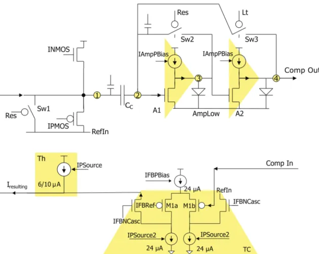
3.2 The Analog Channel of the DCD
Besides the pipeline ADC the analog channel of the DCD consists of further compo- nents shown in Fig. 3.7. One DCD features 256 of such analog channels.
3.2.1 Offset Compensation
A wide spread of the drain currents can be expected among DEPFET pixels. In order to reduce this and fit the drain currents into the dynamic range of the ADC, the DCD provides a two bit wide offset compensation for each channel. TheDACholds three current sources proportional to the global configurable sourceIPDAC. It is foreseen
Figure 3.7:Overview of the analog channel of the DCD. [22]
to measure the pedestal currents for each pixel at a time when no events occur and to store the value in the DHP memory. During data taking, those values are used to control whether three, two, one or none of the sources are added to the signal current of an individual channel. Therefore the pre-stored two bit valuesDAC(0:1) for each individual channel are loaded into the DCD by every new sampling pe- riod.
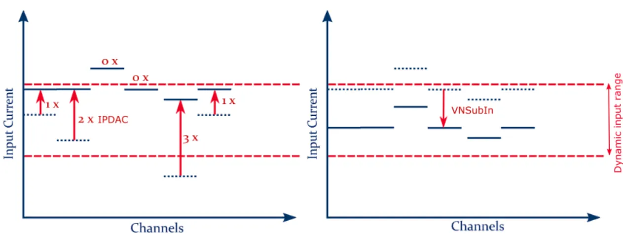
The left side of Fig.3.8 shows how the pedestal spread is reduced in this way. Once signals are on the same level, the global sourceVNSubInsubtracts a current in order to shift the entire distribution into the dynamic input range of the ADCs. In case of cur- rents that are too lowVNAddInis employed. While those sources cover a wide range in coarse steps,VNAddOutandVNSubOutare used for fine tuning directly before the in- put of the ADC.
Figure 3.8:The offset compensation principle. At first the spread among channels is reduced by an individual addition ofIPDAC, then channels are collectively pulled into the dynamic range byVNSubIn.
3.2.2 The Current Receiver
As mentioned before, it is essential for the current memory cells to keep their input nodes at a constant potential independent of the current flowing into it. Usually this is ensured by the output of the previous cell. For the first two cells the resistive current re- ceiver takes on this task.
Its main building block is a transimpedance amplifier (TIA) that converts the input cur- rent into voltage. The TIA’s feedback splits up into two paths, one holding resistance Rf and the other holding capacitanceCf. At its output, the resistanceRs converts the voltage back into current. Cf,Rf andRsare programmable parts and offer the possibil- ity to adjust the receiver. Rf can be switched to either 30 kΩor 60 kΩ, thereby limiting the input dynamic range of the receiver to 16 µA or 8 µA accordingly. In contrast,Rs
defines the output dynamic range, which is 16 µA forRs =15 kΩand 32 µA forRs = 30 kΩ. Changes of the in and output ranges naturally affect the gain. Therefore the gain is defined as
G = Rs
Rf (3.2)
The low pass filter Cf can be set to different values in the range from 60 fF to 460 fF, which can help to reduce noise. This also affects the settling timeτof the TIA, for which
holds
τ =∝ CfRf (3.3)
Moreover the receiver offers an analog common mode compensation. Since this is not used in this work, the interested reader is referred to [22]. A detailed de- scription of all configuration parameters of the current receiver can also be found there.
3.2.3 Calibration and Configuration
The calibration circuits are used for testing purposes (see Fig. 3.7). They can either be connected to the input of the ADC or to the input of the receiver through the global switchAmpOrADC. Besides the global configuration bits, the DCD’s shift register (Con- fig) offers three individual bits for every channel.
EnDCcontrols the channels connection to the monitor pin. This pin can be used for voltage and current measurements as well as for the injection of test signals. There are two possibilities to inject a test current via the monitor pin. Firstly, by connecting an external current source, secondly by using the internal slow current injection of the DCD.
The internal fast current injection, controlled by DACVPInjSigis activated by global bit InjectLocand local bitEnInjLoc. Unfortunately this current source could not be used for this thesis, due to synchronization problems between DCD and DHP.
The third local bitEnCMCactivates the common mode compensation. The pixel shift register can be accessed via JTAG withLd,CkandShEnsignals. For the description of the decoder see section 3.1.2.
3.3 The Digital Block of the DCD
Besides the 256 analog channels, the DCD possesses a large digital block. Among its tasks, the high speed data transmission and the conversion of raw digitization values into standard binary representation are especially interesting in the context of this work.
3.3.1 Data Conversion
For every current sample the pipeline ADC produces eight pairs of output bits (h,l).
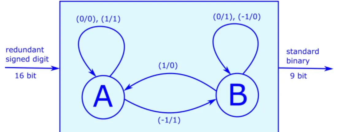
This representation contains redundant information, which is why a conversion into standard binary code reduces the amount of data. Due to the fact that transmission lines between DCD and DHP are limited in space, it is preferred to do the conversion in- side the DCD. Therefore it has a large digital part, which contains a finite state machine as proposed in [24]. Since it uses the Least Significant Bit (LSB) first, the order of the ADC code has to be flipped in a bi-directional shift register before entering the state ma- chine.
Figure 3.9:The state machine converts redundant signed digit code from the ADC into standard binary representation.
The state machine works in synchronization with the ADC. With every clock cycle it takes a new bit pair (h, l) as input, which can be represented as signed number a = h−l ∈ {−1, 0, 1}. This is translated to a single output bit ∈ {0, 1}. The state machine’s logic is depicted in Fig. 3.9. Depending on the state of the system (A or
B), everyin, in this case the stages outputsai, produces a correspondingout(in/out).
Starting from state A, this results in eight bits of output code. An additional ninth bit, which can be interpreted as the sign of the code, is determined by the final state of the system. If the machine ends in state A this will be 0, which stands for positive, if it ends in state B this will be 1, which stands for negative. In this way a nine bit standard bi- nary code, in the range−255 to 255, is obtained out of the 16 bit code, coming from the ADC.
3.3.2 Data Transmission
Since the DCD is specified for a conversion resolution of eight bit, a transmission of nine bit would be a waste of transmission bandwidth. Therefore it was decided to neglect the LSB, in order to reduce the output code to a range of −127 to 127.
The same result could be obtained by reducing the number of the ADC’s conver- sion stages from eight to seven. Nevertheless, for an easier digital design and seri- alization strategy, a reduction of bits was preferred over a reduction of cell blocks [25].
The digitization values are transmitted to the DHP on an eight bit wide output bus, where every bit of the word is transmitted on a different transmission line. Since the number of transmission lines is limited, a further signal serialization is needed. In order to do so, the 256 channels of the DCD are divided in eight groups of 32 channels each. Every group is multiplexed to one eight bit bus, on which the data of its channels is transmitted in series. Consequently, the transmission frequency has to reach 32 times the sampling rate, which adds up to 305 MHz.
In order to test the interaction of the individual PXD components, a test setup was assembled. It features a half ladder prototype plus power supply and first level data processing. The test module is linked to a patch panel via a flexible Kapton cable. From here the data is transferred to the DHE via a 15 m Infiniband cable. The analog and digi- tal supply voltages are generated by the power supply (PS). The setup is controlled by a Scientific Linux 6computer usingEPICSandCS-Studio. The measurement and analysis scripts were written inPhython 2.7.
Figure 4.1:The test setup. The half ladder module is connected via a Kapton cable to a patch panel. From there power and data lines split up to the power supply and the DHE respectively. A computer controls the whole setup.
4.1 Test Modules
The test module is the heart of the test setup. This is a prototype of one of the half lad- ders, of which the final detector will contain 40. The two different test modules, which have been used in this work, are described in the following.
4.1.1 The EMCM Board
The Electronic Multi Chip Module (EMCM) was build for tests of the electric compo- nents. Therefore it is equipped with the full set of ASICs, mounted on a dummy of the true half ladder size. This module does not contain a pixel matrix.
Figure 4.2:A photograph of the EMCM. [26]
4.1.2 The PXD9 Pilot Module
The PXD9 Pilot module is an improved prototype with a fully functional pixel matrix of full size. All kinds of functionality and irradiation tests are possible on this module.
This includes a characterization of the DCD within the detector environment for the first time.
Figure 4.3:Photograph of the PXD9 Pilot module with the full pixel matrix. [26]
4.2 Data Transmission
A stable data connection between the module and the computer has to be guaranteed before performing measurements. Therefore the DHP offers a set of adjustment op- tions.
4.2.1 DCD – DHP Communication
Figure 4.4:Each of the 64 transfer lines can be delayed individually in order to shift the sampling point (blue arrows) to the middle of the signal plateau.
The data of the DCD is transferred to the DHP via eight 8-bit buses on a nominal frequency of 305 MHz (see chapter 3.3.2). In order to ensure highest signal integrity, each of the 64 physical transfer lines can be delayed individually by up to 15 pro- grammable delay elements. Furthermore the global sampling point can be adjusted via a shift of the controlling clock. Fig. 4.4 illustrates how the delay can be used to shift the sampling point towards the middle of the signal plateau. The DCD
offers the possibility to generate a test pattern, which can be used for delay adjust- ment.
4.2.2 DHP – DHE Communication
On the output side the DHP transmits the data via a flexible Kapton cable, the patch panel and a 15m Infiniband cable to the DHE. Over this distance a pre-amplification of the signal is needed to compensate the attenuation of the high frequency component lost during data transmission (see Fig. 4.5). The DHP’s output driver features a pro- grammable preemphasis via three parametersBias,Bias DandBias Delay. A detailed de- scription of the DHP’s output driver can be found in [27].
Figure 4.5:A signal preemphasis is needed to compensate the loss caused by the cable transfer function.
Figure 4.6:Amplitude, overshot and length of the preemphasis are controlled byBias, Bias DandBias Delay.
4.3 Test Sources
In chapter 3.2.3, the calibration circuit of the ADC channel was described. This includes a monitor pin, allowing the connection of a current source for testing purposes (see Fig. 3.7). Due to the chip design, the monitor pin can just be activated for one channel at once, which is controlled by the local variableEnDCin the pixel shift register. At
the same time other channels have to be masked out in the DHP’s memory to allow zero suppressed readout. This is achieved by setting the pedestal threshold of the corre- sponding pixels to 255.
Figure 4.7:The pedestal mask for the internal and external current source plotted in electrical mapping. In this case channel 32 of the fourth DCD is activated. With this mask channel 32 is sampled 192 times within one frame.
4.3.1 The Internal Current Source of the DCD
The DCD features a current source exclusive for testing purposes, which can be con- nected to the monitor pin. Actually it is composed of three DACs, with 127 settings each. For Fig. 4.8 the current source was recorded with a Source Meter/Measuring Unit (SMU). It ranges over 32 µA in 381 steps. The gain was fitted as
(83.236 511±0.026 381)nA/DAC.
Besides a relatively restricted range, the internal current source has one large disad- vantage. The fact that it is controlled via JTAG, necessitates a waiting time after setting a DAC value. It was found out that this has to be 100 ms to work correctly. Hence, the waiting time for the full range sums up to 38.1 s, making a characterization of the DCD with the internal current source very time consuming.
4.3.2 The External Current Source of the DHE
An external source can be connected to the monitor pin also. For this purpose the DHE includes its own current source. With a scope of 248 µA in 65000 steps, it exceeds both the precision as well as the range of the internal current source by
Figure 4.8:The internal current source of the DCD.
far. Moreover this source can be switched much faster, resulting in a measure- ment time of ∼2 s per transfer curve. A fit of the gain yielded a resolution of (3.815 478±0.000 002)nA/DAC.
Also the external current source has a big drawback. While the current source itself shows very low noise, a lot of it is picked up on the path to the module. On the one hand the 15 m Infiniband cable is not designed for current supply. On the other hand the connection on the patch panel is bridged by unshielded wiring. Consequently the transfer curves recorded with the external current source show a much higher noise than those of the internal source.
Figure 4.9:The external current source of the DCD.
4.3.3 DEPFETs as Current Source
So far there has been the choice between a very slow switching and a noisy current source. This is why the idea arose to utilize the DEPFETs as current source.
As every Metal-Oxide-Semiconductor Field-Effect Transistor (MOSFET) the DEPFETs show an increase of the drain current with increasing negative gate voltage. Fig. 4.10 shows the transistor characteristics of the DEPFET. Since the linear range of the ADC is limited, the plot is put together of multiple measurements where different values of the current sourceVNSubInwere added. The area from−1500 mV to−200 mV is more than sufficient to cover the whole input range of the ADCs. In this way the DEPFETs form an additional test current source, which is controlled via the gate volt- age.
When using this source, it has to be ensured that only one matrix row is activated in the DHP memory to guarantee zero suppressed readout. While on the one hand a large
Figure 4.10:Transistor characteristic of the DEPFETs. The red square marks the area used as a test current source. [28]
deviation from linearity must be accepted, the DEPFET current source overcomes the problem of the monitor pin restriction on the other hand. This source can be applied to all channels of all four DCDs of one half ladder at once, resulting in a huge speedup of the ADC characterization.
Figure 4.11:The pedestal mask for the DEPFET source plotted in electrical mapping.
In this case only row 25 is activated for all four DHPs. This results in one reading of each channel per frame.
Characterization
The test setup described in the previous chapter can be used for a characterization of the DCD. The development of sophisticated test methods is motivated by several rea- sons:
Debugging of prototype:
This non-standard chip was specifically designed for the readout of the Belle II pixel detector. DCDBv4 pipeline is the latest release in a long development process, but not yet the serial version for the final detector. Hence it still may contain minor design errors, e.g. mismatching components, leading to defective operation. Thoroughly testing of the chips functionality becomes exceedingly necessary. Especially the testing of the chip within the detector system can provide important feedback, needed for the development of the final DCD version.
Optimization of serial production:
The PXD will contain 160 DCDs, including 40 960 ADC channels with 1.3×10⁶ CMCs and comparators. With regards to this huge number, statistical deviations among cells that lead to defects must be expected. In order to prevent mal- function and to minimize the percentage of non functional channels, individual adjustment of every single DCD’s setting is an essential task.
Readjustment due to radiation errors:
Moreover, the chip will be operated in a radiant environment. Though there is no experience in long term radiation exposure for the DCD, it is save to assume that the chips’ performance will change over time. This effect must
be compensated in order to prevent the PXD from deterioration. This can be achieved by readjustment of the DCD’s settings, but therefore characterization of the chips during the running experiment becomes indispensable.
In consideration of the mentioned challenges, the development of suitable testing and optimization routines for the DCD is a very important task for guaranteeing the full functionality of the PXD. Appropriate tools to characterize the ADCs are so called analog-to-digital transfer curves. Instead of the DEPFET’s signal currents a test current source is applied to the ADCs here. While the current is gradually increased, the digital output codes of the ADCs are recorded. In this way the Digital-to-Analog Converter Units (DACs) of the test source, which correspond to a known current, can be related to the digital output code of the DCD.
Conversion errors can be detected from the comparison of the test current to the digital output. Therefore, the test source should provide a high degree of linearity, as well as a fast switching ability and low noise. Additionally, a higher resolution than the ADC over the full dynamic input range is needed, in order to cover all digitization values (ADU). For the following measurements the current sources described in Chapter 4 were used. Fig 5.1a shows an idealized test current source with the corresponding trans- ferred ADC curve (Fig. 5.1b).
(a) (b)
Figure 5.1:Transfer of a test current into digital code. Every DAC value has been sampled 512 times. The color code in b) marks the number of readings.
5.1 Properties of the ADC Transfer Curves
The properties which are used to evaluate the quality of a transfer curve are described in this section. First of all, it has to be considered, that an ADC converts a continu- ous analog signal into discrete digital numbers. Consequently, a loss of information depending on the ADCs resolution occurs. This so called quantization error is natu- rally to all analog-to-digital conversions. The mean quantization errorσQnoiseis defined by
σQnoise = √∆I
12 (5.1)
where∆I is the current difference of two consecutive steps. This results inσQnoise = 0.3 ADU, which represents the lower limit of noise. In the case of the eight bit pipeline ADC, the conversion results in a staircase with 256 steps (see Fig. 5.2a). Ideally, the step size would be the same for all stairs over the full range. Since this is not always correct, two methods are used to determine deviations.
Integral Nonlinearity
The first method is called Integral Non-Linearity (INL). It describes the divergence between the ideal line transfer function fideal and the actual outputM. Here,Mis the
(a) (b)
Figure 5.2:a) The ideal transfer function of an ADC (4 bit), where the blue line marks the input current. b) A defective transfer function containing deviations in DNL, INL and range.
mean of all readings per DAC.
I NL(x) = M(x)−fideal(x) (5.2)
The ideal line is calculated with the method of least trimmed squares [29], [30]. Com- pared to the standard least squares, this is more robust because outliers are excluded.
For further robustness, only data points at least 10 ADU higher than the minimum and 10 ADU lower than the maximum are considered for the ideal line calculation. Due to the staircase nature of the actual transfer function, the INL typically shows a saw tooth behavior. Absolute INL values higher than 0.5 indicate nonlinearity. Often only the maximum of the INL function is stated, as it is mostly sufficient to rate the linearity of a transfer curve.
Differential Nonlinearity
The second approach, called Differential Non-Linearity (DNL), measures deviations of single step sizes. In ideal case, the step size is exactly the 256th part of the full input
range, which is called the Least Significant Bit (LSB). The DNL is defined as the ratio be- tween the real step size and the ideal value.
DNL(i) = Vi+1−Vi VLSB
−1 for 1≤i≤254 (5.3)
The ideal step sizeVLSBis calculated by the method of least trimmed squares as for the INL.Viis the average DAC value per ADU. DNL values different than 0 indicate de- viations in step size. Absolute DNL values higher than 1 lead to non monotonic transfer functions, also known as missing codes.
Range
Apart from linearity, the quality of a transfer curves also depends on its range.
This may seem trivial, but it turned out that the digital output codes often do not reach the full range of 255 ADUs. Then, the transfer curve is limited at certain ADU values. This can happen at the upper as well as at the lower end. There- fore, the minimum and maximum ADU values are included into the quality con- trol. Notice that the minimal ADU value is 1, while the maximum value is 255.
You may wonder why only 255 values exist, instead of the 256 usual for 8 bit pre- cision. This originates from the fact, that the DCD produces signed output code in the range ±127, involving ±0. The twofold meaning of 0 gets lost in later con- version, where simply 128 is added, leading to final digitization results in range 1 to 255.
Noise
The last evaluation property of a ADC curve is its noise. In order to determine the noise, a statistic of at least 512 samples for every DAC value was measured, where the noise is defined as the standard deviation of the samples. The median noise over the full dynamic range is an appropriate indicator for defect classifica- tion.
5.2 Analog Defects
The properties defined above can be used for defect detection. An overview of the dif- ferent defects types, with an explanation of their cause, is given in the following. It is distinguished between analog and digital defects. Analog defects originate in the ana- log domain of the ADC, where they are caused either by mismatching components or wrong settings.
5.2.1 Limited Range & Gain Deviations
Among the parameters of the DCD, IPSource, IPSource2 and IFBPBias have by far the largest impact on the ADC performance. They have in common, that they do not only influence one type of defect, but multiple. Fig. 5.3 shows how the parameter IPSource affects the range and the gain of a transfer curve. The gain reaches from 0.02 µA/LSB for IPSource=20 to 0.11 µA/LSB for IPSource=120. Ac- tually it was intended to set the gain in the current receiver only, but in fact it turned out that it also scales with IPSource. This is not a defect in the classical sense, but it has to be considered when tuning IPSource in order to fix other de- fects.
The curve reaches a maximum range of 255 ADU for IPSourcevalues from 60 to 80.
Above this, the range rapidly shrinks up to poorly 139 ADU forIPSource=120. Below IPSource=50 more and more errors occur, untill the transfer curve totally collapses atIP- Source=10.
This behavior can be explained in terms of the transfer model (Fig. 5.4). In order to work properly, the size of the cell must cover at least±4Ire f. With increasingIPSource, bothIre fand the thresholds increase. In this way the condition is no longer fulfilled and high currents don’t fit in the cell anymore, which results in a limited range. According to the conversion algorithm, the change of the gain can be explained by the shift of the thresholds.
IPSorce2andIFBPBiascontrol the size of the cell, marked by red in the model (Fig. 5.4).
Fig. 5.5 shows the effect ofIPSource2on the transfer curves. Again, a strong influence
![Figure 3.7: Overview of the analog channel of the DCD. [22]](https://thumb-eu.123doks.com/thumbv2/1library_info/4010086.1541076/41.892.179.645.163.590/figure-overview-analog-channel-dcd.webp)