Cold Electronics for the Liquid Argon Hadronic End-cap Calorimeter of ATLAS
J. Ban,b H. Brettel, W. D. Cwienk, J. Fent, L. Kurchaninov∗ , E. Ladygin,c H. Oberlack, P. Schacht, H. Stenzel,d
P. Strizenecb
Max-Planck Institut fuer Physik, Werner-Heisenberg-Institut, Munich, Germany
bOn leave from Institute of Experimental Physics, Slovak Academy of Sciences, Kosice, Slovakia
cOn leave from Joint Institute of Nuclear Research, Dubna, Russia
dNow at II. Physikalisches Institut, JLU Giessen, Germany
Abstract
This paper describes the on-detector electronics of the ATLAS hadronic end-cap calorimeter (HEC). The electronics is operated in liquid argon; therefore attention is paid to its performance at low temperatures. The core of the electronics are Gallium Arsenide (GaAs) preamplifiers. We present design, layout and results of various tests of the preamplifier chips and summing boards. The calibration and signal cables have been studied in laboratory conditions and the signal distortion is modeled. All parts of the electronics have been produced, tested and assembled on the calorimeter modules. The summary of the commissioning tests is presented.
Key words: Low temperature electronics, Front-end, GaAs amplifier PACS:07.50.Yd, 29.40.Vj, 84.30.-r
1 Introduction
The ATLAS calorimeter covers the range in eta up to|η|<5. For the hadronic calorimetry different techniques are used matched to the different requirements and radiation levels. Thus in the central and outer forward region (|η| <1.6) the scintillator-iron tile technique is used. In the forward region the liquid
∗ Corresponding author. Tel.: +4122-7676518, CERN CH-1211 Switzerland Email address: Leonid.Kurchaninov@cern.ch (L. Kurchaninov).
argon (LAr) technique is employed: the end-cap cryostat contains the elec- tromagnetic calorimeter (EMEC), the hadronic calorimeter (HEC) and the very forward electromagnetic and hadronic calorimeter (FCAL). The EMEC and HEC are structured in one and respectively two wheels. The FCAL is a high density calorimeter with rather small LAr gap size. For the EMEC and FCAL the signal amplification is done in warm with the electronics positioned at the feedthroughs. For the HEC the signals from individual cells are am- plified and summed to the related read-out channels in the cold, minimizing the noise contribution. This paper describes the cold electronics components of hadronic end-cap calorimeter.
2 The Hadronic end-cap Calorimeter
HEC is a liquid argon ionization detector with copper plate absorbers. It consists of two wheels, the front HEC1 and rear HEC2, each wheel is made of 32 modules, so the calorimeter has in total 64 front and 64 rear modules [1], [2].
A full azimuthal (φ) wedge of a front and rear module has 40 liquid argon gaps.
The gaps are instrumented with read-out structures consisting of one central pad-board and two electrostatic transformer electrodes each. All electrodes are covered with high resistive layers, made of carbon-loaded kapton with a typical surface resistance of ∼1MΩ/2.
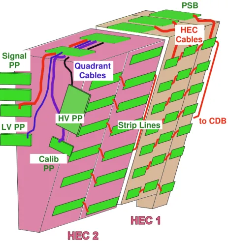
The general layout of the cold electronics components is shown in the Fig.1.
The read-out pad-boards are connected via gold plated pins to strip-lines fixed with gold plated screws to the copper plates at both sides of the HEC modules. The strip-lines are kapton based printed circuit boards with gold plated electrodes. They carry the signal and calibration lines and they are designed to have wave impedance of 50 Ω. Two consecutive gaps feed finally into one coaxial cable, transmitting the signal to the preamplifier. The strip- lines distribute also the calibration pulses which are injected at the pad-board level through 5.6 kΩ precision resistors.
The preamplifier and summing boards (PSB) equipped with GaAs preamplifier chips (Section II) are installed on the outer radius of the calorimeter wheel inside the cryostat within the LAr. The connections between the strip-lines and the input of the preamplifiers as well as the distribution of the calibration pulses are performed by a set of patch panels and coaxial cables.
The size of readout cells (pads) is ∆η×∆φ = 0.1×π/32 in the low η region and 0.2×π/16 in the inner region. The most outer pads have larger area and therefore larger capacitance. These pads are divided in two sub-pads in order
to CDB PSB
LV PP
Calib PP Signal
PP
HEC Cables
Quadrant Cables
HV PP
Strip Lines
Fig. 1. The electronics components of the HEC modules. All patch panels (PP) are placed at the back side of the HEC2 wheel. The signal side cables connect pad-boards and PSB inputs. The quadrant cables connect the PSB outputs (the calibration distribution board, CDB) with the signal (calibration) patch panels.
to minimize the overall spread of input load of preamplifiers. The detector capacitance varies from 40 to 450 pF that gives rise time variation from 5 to 25ns.
The signals from a set of preamplifiers (2, 4, 8, or 16 for different regions of the calorimeter) are then actively summed forming one output signal, which is transmitted to the cryostat feed-through by another set of cables and dis- tribution boards. All cables and lines have 50 Ω wave impedance.
The HV is connected to the PAD and EST boards using the strip line con- necting technique. For safety and to limit the voltage drop due to current, two connections per electrode are used. The ground of the external feeding HV line is connected to the cryostat, which is thus acting as a Faraday cage. In the Filter box at the cryostat feedthrough two resistors (200 kΩ and 5 kΩ) for each HV line are added in series with a capacitor of 27 nF in between connected to ground.
At the HEC HV patch panel another series resistor of 100 kΩ is added in each line. This line is finally connected to the strip line connectors which dis- tribute the HV to the electrodes of one longitudinal segment. Each electrode is connected with small tabs to the strip line connector. Just before this con- nection, a resistor of 500 kΩ is added in series. The distribution of the HV on the electrode is done with high resistive polyimide layers with a resistivity of typically 1 MΩ/2. This scheme has shown to be very effective in suppressing any HV induced noise in the readout. The resistivity of the polyimide layers limits also any current due to potential electrical discharges to a low value, safe for the cold electronics.
3 GaAs Preamplifiers
The GaAs TriQuint QED-A 1µm technology has been selected for the front- end ASIC because it offers excellent high frequency performance, stable oper- ation at cryogenic temperatures and radiation hardness.
The front-end chip consists of 8 identical preamplifiers and two drivers. This design gives the possibility to sum signals of either 4 or 8 channels according to physics requirements. The summing scheme is implemented with external components and interconnections made on the PSB.
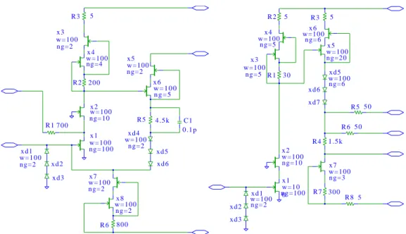
The Fig.2 shows the circuit diagram of the preamplifier and driver. The input stage X1, X2 is a cascade, biased by two current sources X3, X4 and X7, X8. The diodesXd1 - Xd3 protect the input transistor against possible high voltage discharges in a LAr gap [3]. The first transistor has the effective width of 10 mm (100 gates of 100 µm in parallel) in order to optimize the noise performance. Its forward conductance can be adjusted by applying additional current through the resistorR1. The feedback loop is formed by the combina- tionR5 -C1. Together with the open-loop gain its value determines the input impedance, which is close to 50 Ω. The last stage X5, X6 has high output impedance, so current signals can be summed at the external load resistor.
In addition, three diodes Xd4 - Xd6 ensure the level shift and temperature stabilization. The temperature stabilization scheme is based on the fact that the temperature dependence of the voltage on the forward biased diode and the pinch-off voltage of the transistors used have opposite sign. The pinch- off voltage is monitored by R6 and amplified by R5. The total voltage on the three diodes in series together with the voltage on R5 will stabilize the working point of X6 over a large temperature range.
The driver scheme is similar to the preamplifier one, but with an external feedback loop. By choosing the driver feedback components properly one can
w=1 0 0 n g=2 x 3
x 4 w=1 0 0 n g=4
2 0 0 R 2
w=1 0 0x 2 n g=1 0
w = 1 0 0 n g= 5 x 6
R 5 4 . 5 k 7 0 0
R 1
x d 3 x d 2 w=1 0 0 n g=2 x d 1
R 6 8 0 0 w=1 0 0x 8 n g=2
x d 6 x d 5 w=1 0 0
n g=2 x d 4 x 5 w=1 0 0 n g=2
w=1 0 0x 7 n g=2
0 . 1 p C 1 R 3 5
x 1 w=1 0 0 n g=1 0 0
x 1 w=1 0 n g=1 0 00 x 3
w=1 0 0 n g=5 R 1 3 0
x 5 w=1 0 0 n g=2 0
x 2 w=1 0 0
n g=1 0 x 7
w=1 0 0 n g=3 x d 6 x 4
w=1 0 0 n g=5
1 . 5 k R 4
3 0 0 R 7
w=1 0 0 n g=6 x d 5
x d 7 w=1 0 0x 6
n g=6 R 3 5
x d 3 x d 2
w=1 0 0 n g=2 x d 1
5 R 2
5 0 R 5
5 R 8
5 0 R 6
Fig. 2. Circuit diagrams of the GaAs preamplifier (left) and driver (right).
adjust the overall gain and timing. The chip has dimensions of about 4 × 3 mm2. It is housed in a standard square 40-pin leadless ceramic package.
Several chips from the preproduction batches have been used for a detailed study of signal and noise characteristics both at room and cryogenic temper- atures. Here we only present results obtained at low temperature, mainly in liquid nitrogen.
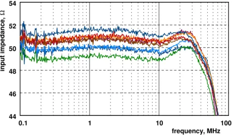
The input impedance measured with a network analyzer is shown in the Fig.3 for 8 preamplifiers from three different chips. The drop at high frequencies is due to the gate capacitance of the head transistor, the feedback capacitance and the connecting cables. For 10 preproduction chips (80 preamplifiers) the input impedance varies from 48 to 52 Ω in the working frequency range around 10 MHz.
Fig.4 shows the typical response to an exponential calibration signal. The mea- surements of rise time and amplitude with different input (detector) capacities give the amplification factor and values of leading and second poles.
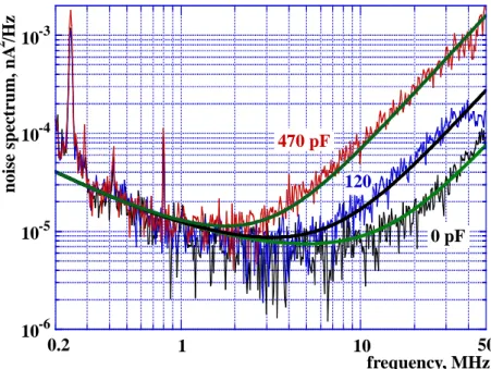
The noise spectrum measured with different input capacitors is presented in the Fig.5. The low frequency 1/f component with a typical value of the flicker noise corner frequency 1.0−1.5MHzcan be seen. The serial and parallel noise values correspond to thermal noise of equivalent resistorsRns= 35−40 Ω and Rnp = 0.5−0.6 kΩ respectively (solid lines). These values are used for the predictions of the signal to noise ratio (see Section 7).
In the hadronic end-cap calorimeter a neutron fluence of 0.3×10¹⁴neutrons/cm2 is expected after 10 years of LHC operation at high luminosity. It is known
0.1 1 10
frequency, MHz 44
46 48 50 52 54
input impedance, Ω
100
Fig. 3. Absolute value of the input impedance vs. frequency for 8 preamplifiers from three different GaAs chips.
time, ns
voltage, mV
-10 10 0 20 30 40 50 60 70
0 100 200 300 400 500 600
Fig. 4. Output waveform measured with an exponential input signal.
that GaAs is a radiation resistant semiconductor, nevertheless the radiation hardness has been studied at the IBR−2 reactor in Dubna, Russia with a set of pre-production chips.
Various types of tests have been performed. Seven chips were exposed to the total fluence of fast neutrons of (1.11±0.15)×1015 n/cm2 and an integrated γ dose of 3.5±0.3 kGy. A second set of 8 chips was irradiated with γ’s up to a total dose of (55± 8) kGy accompanied by a fast neutron fluence of (1.1±0.2)×1014 n/cm2. In these tests the chips were kept in a cryostat filled with liquid nitrogen.
The standard set of characteristics like transfer function, rise time, linearity and equivalent noise current (ENI) of preamplifiers was measured. The mea-
10-6 10-5 10-4 10-3
noise spectrum, nA /Hz2
1 10
frequency, MHz
0.2 50
120
0 pF 470 pF
Fig. 5. Measured (points) and calculated (solid lines) noise spectrum for detector capacities of 0, 120 and 470 pF respectively.
1013 2 3 4 5 6 7 81014 2 3 4 5 6 7 81015
neutron fluence
0.6 0.7 0.8 0.9 1.0
Cd = 10 pF Cd = 100 pF Cd = 220 pF Cd = 330 pF
amplitude ratio
Fig. 6. The signal amplitude measured after values of neutron fluence from 1.5×10¹³ to 9×10¹⁴n/cm2 for 4 different detector capacities. Shown is the ratio to the signal amplitude before the irradiation.
surements show that the preamplifier characteristics start to degrade when the neutron fluence exceeds approximately 3×10¹⁴ n/cm2. The Fig.6 shows the degradation of the amplitude with neutron irradiation for four different values of input (detector) capacitance. The measurements were performed with a rectangular input pulse and a RC2−CR shaper with a time constant of 20ns.
Similar measurements with γ- irradiation show that the characteristics stay unchanged up to a dose of at least 50 kGy. Both boundary values are well
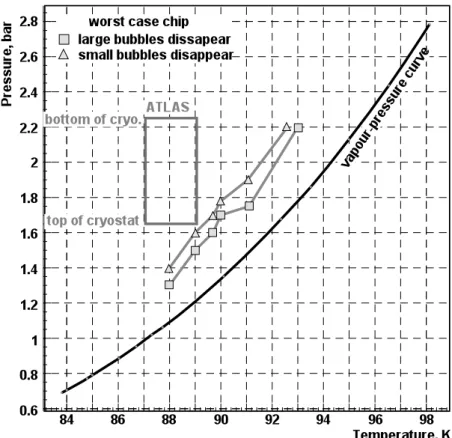
Fig. 7. Area of LAr bubbling due to the heating by the preamplifier chips.
above the radiation levels expected in the final ATLAS environment.
Another important practical aspect of the cold electronics is the heating of the chips that can finally result in bubbling of the liquid argon. The bubbles propagating to a LAr detector gap can cause high voltage discharges or break- downs. The bubble formation has been studied with pre-production chips. The Fig.7 shows the area of pressure and temperature space where bubbling takes place.
The box in the Fig.7 presents the area of LAr pressure and temperature ex- pected in the ATLAS end-cap cryostats. The most critical bottom area of the calorimeter corresponds to the top part of the red box. In this regime the bubbles creation point is far away from the LAr operation point.
4 Production and quality assurance of the preamplifiers
The hadronic end-cap consists of 64φ-wedges in four calorimeter wheels. One wedge is equipped with a group of 5 PSB’s (see next section), all together con- taining 67 GaAs chips. The total PSB production volume contains 64 groups for the whole calorimeter and a spare set of 11 groups. In total 5025 GaAs
chips are required for this production volume.
The production run of 20 GaAs wafers (570 chips per wafer) has been made in August - September 1998. In total 16 wafers have been cut and packaged. The chips have been tested by the manufacturer and 6600 chips have been delivered by the end of 1998. The in-factory tests include the wafer parameters, the shorts and opens, the bias currents, the potentials at the input, output and floating pins.
Before assembly on a PSB all delivered chips passed quality assurance tests, consisting of measurements of functional parameters. Before the measurements all chips passed a temperature shock cycling to guarantee no failures during future cooling down and warming up cycles. All preamplifiers were dropped into liquid nitrogen, kept there 30 minutes and then taken out and dried by compressed air. This operation was repeated five times. To study the effect of the temperature cycling, the chips from the preproduction batch have been measured twice, before and after the shock test. It was found that only 1% of the chips were damaged. In order not to double the amount of measurements, we made all tests only after the temperature cycling for the final production batch.
The measurements of electrical characteristics have been performed under conditions close to real input and output loads. An exponential signal with 360nsdecay time was injected to the preamplifier input via a 5.1kΩ resistor.
The preamplifier input is loaded via 1 mcoaxial cable (the same type as used in the final production) and 220pF capacitor, representing the calorimeter impedance. The output signal is shaped by a RC2 −CR filter with a time constant of 25 ns and an amplification factor of 10.
The measured characteristics are signal amplitude, peak time, noise RMS value, nonlinearity and crosstalk between neighbouring channels. The param- eters were measured with a Tektronix TDS540 digital oscilloscope by switching input signals sequentially with a Keithley scanner Model 705 . The tests were made using specially designed boards housing up to 4 chips and having the same passive components as on the final PSB.
All measurements were performed at room temperature since the standard sockets used on the test board are not designed to work at cryogenic temper- atures. They are destroyed after a few cooling cycles and do not guarantee reliable contacts once placed in liquid argon or nitrogen. Originally the speci- fication parameters of GaAs amplifiers have been developed for LAr temper- ature and can not be applied directly to normal conditions. The parameters were recalculated to room temperature on the basis of measurements of the preamplifier characteristics made in cold and in warm.
There are three different types of summing configurations, applied in different
IN 1 IN 2 IN 3 IN 4
IN 5 IN 6 IN 7 IN 8
OUT 1
OUT 2
IN 1 IN 2 IN 3 IN 4
IN 5 IN 6 IN 7 IN 8
OUT 1 PA
PA
DR
DR
PA
PA
DR
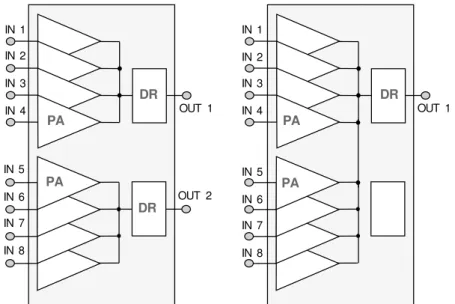
Fig. 8. Different summing configurations used in the HEC read-out channels and implemented in QC tests.
regions of the calorimeter: 4 preamplifiers per output, 8 preamplifiers per out- put and 16 per output. Preamplifiers connected to one driver should have the same gain within 1 %. The uniformity of response is important because in the HEC calibration scheme it is not foreseen to calibrate individual preamplifiers (see Section 6). We define the uniformity as follows:
U(A) = 100%max(A)−min(A)
mean(A) (1)
where the maximum, minimum and mean values are calculated for all pream- plifiers connected to one driver.
The measurements were done first in the configuration of summing 4 pream- plifiers (left plot in the Fig.8). But this measuring scheme can not guarantee the uniformity of the response in the case of summing 8 inputs (see Fig.8, right plot) since the contribution of the preamplifiers 5-8 and the driver 2 can not be separated. Therefore we made a second measurement for each chip on a separate test board, where the summing scheme of 8 channels is realized. In order to save time, only the signal amplitudes were measured in this test.
In each of these two independent tests the chip is characterized as DEAD (D) if one or more channels are dead (amplitude is below 30 mV) and as GOOD (G) if all QC parameters are within a specified window. Otherwise it is characterized as FAIL (F). Chips which are qualified as good in both tests are accepted for the PSB production. There is a fraction of chips which passed the tests with summing 4 inputs, but they did not pass the second test due to non sufficient uniformity of all 8 channels. These chips were accepted for PSB channels with summing 4 inputs only.
There is a small number of HEC channels where 16 preamplifiers are summed.
These channels require 2 chips with the same response functions. The pairs of chips have been selected for these channels by analyzing off-line the uniformity of 16 amplitudes.
In total 6478 chips have been tested, 970 of them have been rejected, 4132 accepted to sum 8 input signals and 1376 could be used for summing 4 pream- plifiers. The overall yield of the QC tests is therefore 85%. The main rejection factor was uniformity of the response over 8 channels of the same chip. The amount of accepted chips is 10% more than needed for the production of the PSB’s.
5 Preamplifying and summing boards
The GaAs chips were mounted on the PSB boards together with the passive components for the interconnections, feedback of driver stages and line filter- ing. As the summing of signals is different in the four longitudinal read-out segments, there are different types of PSB’s. They are specific designs for the first segment, second (two different boards), third and for the fourth one. The basic design is the same for all types of PSB’s but the number of chips and routing of input lines are different.
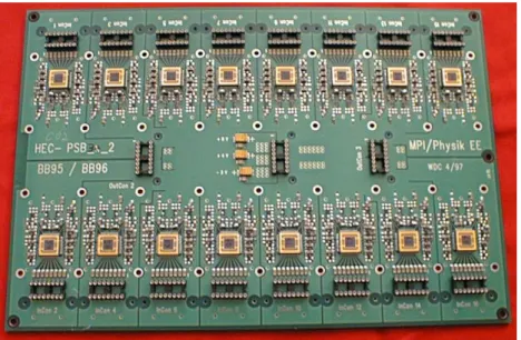
One PSB (for the second segment) is shown in the Fig.9. The low-voltage connector is placed in the center of the board between the output connectors (1 in type B, 2 in type C, and 3 in other PSB types). The input connectors are placed at the left and right sides of the board. The GaAs chips are mounted near the input connectors.
The design of the 8-layer boards took care to separate the signal lines well and make them as short as possible. The interleaved ground and supply voltage planes are segmented, thus avoiding uncontrolled current flow resulting in cross talk or oscillations.
The design has been done in 1996 and the PSB’s have been produced in 1999. The mounting of components and the quality assurance tests have been performed at MPI. The production was completed in 2000 and the tests have been performed during 1999-2002. A set of 20 boards from the preproduction batch has been extensively used in cold and beam tests of HEC modules in 1999-2004 (see Section 8). By now all PSB’s are installed on all HEC wheels.
The quality assurance tests were performed in two steps. Functional tests were performed immediately after production in order to check dead or weak channels. Bad PSB’s were returned to the workshop. If all channels were good
Fig. 9. Picture of the PSB type C.
the PSB’s were kept for the final QC tests. A PSB was stored for future assembly if it passed this test stage.
The simplified functional test consists of measurements of the transfer function (amplitude and rise time) and noise RMS value after theRC2−CRshaper for each PSB input channel. The test bench is similar to that used for the chips quality assurance test, but extended to serve more channels. In a first step the signals and noise were measured at room temperature. If all parameters were within specification, the PSB was remeasured in liquid nitrogen. In this step we also measured the linearity of each channel.
During the tests, 33 GaAs chips with one dead input or one nonfunctional output have been identified and replaced. In addition, 24 passive components were either damaged or not properly soldered. In total, 48 (of 375) PSBs required some rework.
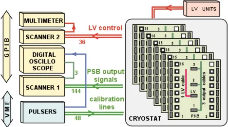
The final QC test of a PSB is a detailed measurement of all electrical character- istics both at room temperature and in liquid nitrogen. These measurements were performed in a small cryostat equipped to house up to 6 boards. The Fig.10 shows the block diagram of the test setup.
Input signals were generated by a pulser board controlled via a VME bus. The signals were distributed inside the cryostat to the PSB inputs via a passive resistive network, placed on a specially designed calibration board (not shown in Fig.10). The PSB inputs are loaded with a 1m coaxial cable terminated by a 220pF capacitor to reproduce a typical detector impedance. These elements were also mounted on the calibration board.
The output signals were read out by three channels of a Tektronix TDS 510A
Fig. 10. Setup of the PSB quality assurance test.
digital oscilloscope, connected sequentially to the PSB output lines through a Keithley scanner 7002 with 9 relay cards (scanner-1 in the Fig.10). The temperature inside the cryostat was measured by two sensors and recorded in all steps of the measurements. The bias voltages were applied from a set of low voltage units. All voltages and currents were measured and recorded individually for each PSB (Scanner-2 and Multimeter in the Fig.10).
In the first step signal and noise were measured at room temperature. If the PSB passed this test, the cryostat was cooled down and the same measure- ments were performed at liquid nitrogen temperature. This test was repeated twice with nominal bias voltages and with boundary values (0.9 and 1.1 of nominal bias). This second test was performed to guarantee the specified work- ing range of the PSB. The final step was the measurement of the linearity and inter-channel crosstalk.
The digitized waveforms were analyzed on-line and the parameters were recorded to files, one file per PSB. These tables were analyzed off-line and the results were loaded to the HEC production data base. Each PSB input channel was specified by gain, rise time, nonlinearity and noise RMS. In addition, each PSB output channel was characterized by average gain, uniformity (as defined in Eq. 1), integral nonlinearity and crosstalk value.
The boards, which did not pass the quality tests, were studied in more detail to identify the source of problems. 9 chips with week output driver and 18 chips with one bad input channel were found. These 27 boards have been returned to the workshop for replacement of components. The tests were finished in 2002 and 64 PSB’s of each type were selected and installed in the HEC wheels.
6 Calibration and signal lines
The knowledge of ionization and calibration waveforms is important for the precise calibration of the detector and thus the accurate energy reconstruction.
The calibration signal is injected at the pad level to a group of four pream- plifiers. It is supposed that these preamplifiers have equal response function, that is guaranteed by chips quality assurance (see Section 4).
The calibration signal propagates through a set of cables, therefore its shape in the injection point is determined not only by the preamplifier transfer function but also by distortions in cables, strip-lines and patch panels.
Various measurements done during beam tests and during cold tests for HEC module acceptance, show that the strip-lines and patch panels are well de- signed to do not disturb neither the calibration nor the output signals. But the signal shape distortion due to skin effect in the coaxial cables is significant and can not be neglected.
The cable characteristics were extensively studied at liquid nitrogen and at room temperatures. Three batches of cable sets from different production rolls have been used. The serial resistance of the central wire determines the attenu- ation of the propagating signal. This resistance has been found to be 0.99 Ω/m at room temperature, which is very close to the factory specification. At LAr temperature it is measured as 0.24 Ω/m.
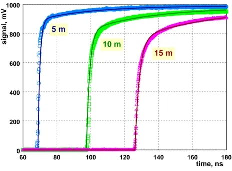
The signal distortion was measured by injecting rectangular pulses from a 50 Ω generator. The Fig.11 shows the leading edge for different cable lengths.
The typical length of the calibration lines in the HEC is about 13 m and the signal cables are as long as 9m. It can be seen that cables introduce significant changes in rise time and attenuation of the HEC signals.
The cable impulse response can be approximated in the frequency domain by a one-zero and two-pole function with the proper attenuation factor:
FC(s) = a 1 +sτZ
(1 +sτP)(1 +sτO) (2)
The values of the three time constants in eq. (2) depend on the cable length and temperature. They are determined from a fit to the experimental data.
The solid lines in the Fig.11 show the result of the optimization.
It has been confirmed that both calibration and signal lines in the real HEC setup are perfectly terminated with 50 Ω impedances, therefore the model function eq. (2) is applicable for calculations of ionization and calibration signal shapes.
60 80 100 120 140 160 180 time, ns 0
200 400 600 800 1000
5 m
15 m
signal, mV 10 m
Fig. 11. The transfer function of terminated cables measured at cryogenic temper- ature (points) and calculated with the model function (solid curves).
Rgi
50 10p
Cg Rs2
50 Rt2
25 Rt3 25 Rt4 25
Rs3 50
25 Rt1
4.5k Rf
0.01p Csl
Rd 50 Rg
0.3u Cdo 0.3u
Ca PTcal
PTsig Qcal
Cal 3
Cal2
Cal1
Qsig -90
Ct 50p Cd
214p
HSig
0.315 1 + s*4n Lg
1+s*24.5n (1 + s*1.2n)*(1+s*28.5n) 5.62k Rc
1+s*18n (1 +
s*1.2n)*(1+s*21.8n) 50 Rs 1
50 Rpi
DET
1.97
Igen 10uH
Cal Gen
CALIBRATION CHAIN CDB
COLD ELECTRONICS SL PSB
L1
L3 L2
0.3u Cdi
150 Rdi
Fig. 12. Schematic diagram of the HEC calibration and signal chains. All parameters are nominal at LAr temperature. The cables are modeled with one-zero and two-pole functions.
7 Model of the electronics chain
The description of the electronics chain response is required for the calibration and physics data analysis [4], [5]. It is also useful to identify and locate possible malfunctioning parts. The scheme shown in Fig.12 represents the calibration and signal chain elements inside the cryostat.
There are two possibilities to model the analog electronics: either to describe the transfer function analytically or numerically (PSPICE simulations). For the calibration procedure an analytical function is required to fit the signal shape. Therefore a PSPICE model can not be used.
The function derived from the diagram of Fig.12 represents the main elements of the chain only. Second order effects could in principal also be described analytically, but the increasing number of poles and zeros leads to a dramatic rise of time-domain expressions and increase of computing time.
The model function of the calibration signal injected at the pad-board level is:
IC(s) =IGRLaC 3RC
(α+sτC)(1 +sτZC)(1 +sτSL)
s(1 +sτC)(1 +sτP C)(1 +sτOC) (3)
The amplitude of the injected calibration current is determined by the gen- erated value IG, the pulser load RL (partly determined by the cable serial resistance), the attenuation in calibration cables aC, the splitting in the cal- ibration distribution board (factor 1/3) and the calibration resistor RC. The first zero and two poles describe the pseudo-exponential shape of the calibra- tion current at the pulser output. The second zero and last two poles represent the cable transfer function, see eq. (2). The last zero describes the parasitic capacitance of the strip-line. In most cases this last factor is negligible.
The signal chain, common for both calibration and ionization signals, can also be modeled by a set of zeros and poles:
HC(s) = RPaS(1 +sτZS)
s(1 +sτA)(1 +sτD)(1 +sτOS)(1 +sτP S) (4)
The overall gain is determined by a preamplifier transfer factor RP and by a cable attenuation factor aS. The first two poles are leading and second preamplifier poles. The zero and last two poles are the signal cable model function, see (2). The decoupling capacitors at the preamplifier input and output produce time constants far from the working frequency range, they are not included in the chain model function.
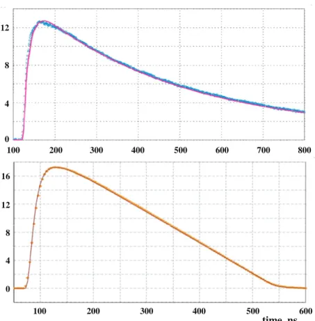
The calibration waveform can be calculated by convoluting the calibration current (3) and the chain transfer function (4) in the time domain. In a sim- ilar way, the ionization signal is the convolution of the triangular ionization shape with (4). The Fig.13 demonstrates the quality of the signal prediction.
Typically the residual of the amplitude between the measured and calculated pulse shapes does not exceed 1%.
100 200 300 400 500 600 700 800
100 200 300 400 500 600
time, ns
0 4 8 12 16 0 4 8 12
Fig. 13. Example of a calibration (top) and ionization (bottom) shape measured at the cryostat feedthrough (points) compared to the calculated waveforms (line) using functions (3) and (4)
Fig. 14. Block diagram of the electronics chain used for the noise calculations.
A model to predict the noise can be built using the same simplified chain function. The block diagram of the Fig.14 shows the electronics components relevant for the noise calculations. The capacitors CD and CA represent the detector and the input transistor respectively. The HEC cable, connecting strip-lines and PSB, is quite short and can be considered as an ideal trans- mission line. The preamplifier is considered as a current sensitive loop with feedback resistor RP and input impedance of 50 Ω.
All transfer functions are summarized in the block H(s) which contains the cold part (4) and the warm part of the chain, which is not described here. The
warm part consists of a preshaper with pole-zero cancelation of the preampli- fier rise time and an RC2-CR shaper.
The noise sources eS and iP represent serial and parallel noise components with spectral densities shown in Fig.5. The noise spectrum at the preamplifier output can be written as:
d dfiN2 =
¯¯
¯¯
¯
1 +iωRA(CA+CD) 1 +iωRA(CA+CC)
¯¯
¯¯
¯
2Ã
4kT RN P
µ
1 + ωS w
+ 4kT RN Sω2|CA+CC|2
!
(5)
The frequency dependent imaginary part of the cable conductance CC de- scribes reflections in the HEC cable. The values of equivalent noise resistors RN S andRN P as well as flicker noise corner frequencyωS are defined in section 3.
Using (5) the noise spectrum can be calculated at any point of the chain, applying the proper transfer function. At the chain output, where signals are digitized, it is:
SE(ω) = d
dfiN2|H(iω)|2 (6)
Finally the noise RMS value can be calculated from the integral of (6) over the full frequency range. The noise autocorrelation function is important for the further digital signal processing. It is calculated as Fourier transform of (6). The Fig.15 shows the noise RMS measured for all channels in one of the HEC beam tests vs. predicted values calculated with the theoretical values of detector capacitance and HEC cable length. The theoretical and experimental values of noise correlation coefficients for a few HEC channels are shown in the second plot of Fig.15.
As can be seen, the noise model yields a high quality prediction of both the absolute noise and the correlation function. Typically the measured RMS is slightly higher than the prediction. This could be due to contributions of second stage electronics which is not included in the model (5).
8 Experience from commissioning tests
A set of 20 PSB’s has been extensively used during the years 1998-2004 in more than 10 beam tests, 3 technical tests and in production cold tests of series HEC modules [6], [7]. For more than 30 cooling cycles, only 6 failures of preamplifiers input channels have been detected.
20 40 60 80 100 120 140 160 expected ENI, nA 20
40 60 80 100 120 140 160
measured ENI, nA
0 50 100 150 200
time, ns -0.4
-0.2 0.0 0.2 0.4 0.6 0.8 1.0 1.2
expected ch. 25 ch. 29 ch. 33 ch. 37
noise correlation function
Fig. 15. Noise RMS in units of equivalent input current (left) and noise correlation function (right) as measured (points) and predicted (line) for some HEC channels.
A special long-term cold run has been made to study the stability of the HEC electronics. In this run, performed in 1998, two HEC modules have been equipped with 136 read-out channels. The system was operated during more than 100 days. Every 12 hours the gain, linearity and noise were measured. In total 214 measurements were done.
The Fig.16 shows the measured amplitude and noise RMS of one of the chan- nels. No systematic drift of the preamplifier characteristics was observed dur- ing the test. The amplitude variations for all channels was 0.64%, including contributions from the calibration system and warm electronics. The noise performance was very stable, no excess noise was observed.
Assembling of four HEC wheels has been performed in the years 2002-2004.
The Fig.17 shows the HEC-2 (rear) wheel assembled on the assembly table in the horizontal position. Clearly visible are the PSB boards with the cold elec- tronics at the outer circumference. After rotation the wheels have been inserted in the end-cap cryostats. All these operations are finished in the meantime.
Finally both cryostat has been cooled down and filled with LAr (end-cap C in March and end-cap A in August 2005). The HEC wheels have been tested following rather similar procedures as done for the individual module cold tests. In total we found 5 disconnected signal lines and 4 read-out channels where one preamplifier was not operational. With 6144 read-out channels in total, this corresponds to a failure rate at the 0.1% level. In addition, 2 dead calibration sub-lines (of 2944) has been detected, corresponding to less than 0.1% level of failure rate.
20
transfer function, kΩ
24 28 32 36
20 40 60 80 100 120 140 160 180 200
run number 3.2
3.4 3.6 3.8
noise RMS, mV
Fig. 16. Amplitude (top) and noise RMS (bottom) vs. run number (time) measured for one HEC channel in the long term run.
Fig. 17. HEC rear wheel assembled and prepared for insertion to cryostat.
9 Conclusions
The HEC cold electronics has been designed to meet the strong requirements of operation for more than 10 years in the high radiation, high rate and low temperature environment of ATLAS. Various laboratory studies and quality assurance tests demonstrated that the produced chips and boards have char-
acteristics close to the design values.
Several years of beam tests and production tests of the HEC modules as well as commissioning of all ATLAS end-cap wheels show the reliable and stable operation of the HEC cold electronics.
Acknowledgements
The development and deployment of the HEC cold electronics has been carried out within the framework of the ATLAS LAr HEC Collaboration headed since 2001 by C.Oram (TRIUMF). We are grateful for the constant support and encouragement.
We acknowledge detailed discussions and friendly criticism by D.Camin (INFN Milano) in the development stages of the project.
This project has been supported by the Bundesministerium fuer Bildung, Wis- senschaft, Forschung und Technologie, Germany, under the contract number 05 HA8EX1 6. We thank the funding agency for the financial support.
References
[1] ATLAS Liquid Argon Calorimeter Technical Design Report, CERN/LHCC/96- 41 (1996).
[2] M. Fincke-Keeler, The ATLAS Hadronic Endcap Calorimeter, Proceedings of the 10th International Conference on Calorimetry in Particle Physics, (2002), 712, Pasadena, USA, 25.3.-29.3.2002.
[3] H. Brettel, D. Kalkbrenner, P. Schacht, Spark Discharge in Normal and High Resistive Coated Electrodes, ATLAS Internal Note ATLAS/LARG Note-46 (1996) [4] L. Kurchaninov, P.Strizenec, Calibration and Ionization Signals in the Hadronic End-Cap Calorimeter of ATLAS, IX International Conference on Calorimetry in High Energy Physics, Annecy, France, 9-14 October, 2000, Frascati Physics Series Vol. XXI, 219-226, 2000.
[5] H. Brettel et al., Calibration of the ATLAS Hadronic End-Cap Calorimeter, Proceedings of the Sixth Workshop on Electronics for LHC Experiments, Krakow, Poland, September 11-15, 2000, CERN/LHCC/2000-041.
[6] B. Dowler et al., Performance of the ATLAS hadronic end-cap calorimeter in beam tests, Nucl. Instr. and Meth.A482 (2002), 94.
[7] C. Cojocaru et al., Hadronic calibration of the ATLAS liquid argon end-cap calorimeter in the pseudorapidity region 1.6 <| η |< 1.8 in beam tests, Nucl.
Instr. and Meth. A531 (2004), 481.