ATL-LARG-PUB-2015-001 17/07/2015
ATLAS NOTE
ATL-LARG-PUB-2015-001
17th July 2015
Upgrade plans for the Hadronic Endcap Calorimeter of ATLAS for the high luminosity stage of the LHC
Faig Ahmadov
a, Teresa Barillari
b, Mircea Cadabeschi
c, Alexander Cheplakov
a, Ruben Dominguez
d, Alexander Fischer
b, Jörg Habring
b, Armen Hambarzumjan
b,
Namig Javadov
a, Andrey Kiryunin
b, Leonid Kurchaninov
e, Roy Langsta ff
e, Mark Lenckowski
e, Sven Menke
b, Ignacio Molinas Conde
b, Martin Nagel
b, Horst Oberlack
b, Michel Raymond
f,
Olaf Reimann
b, Peter Schacht
b, Pavol Strizenec
g, Sven Vogt
b, Giselher Wichmann
baJINR, Dubna, Russia
bMax-Planck-Institut für Physik, München, Germany
cUniversity of Toronto, Canada
dUniversity of Arizona, USA
eTRIUMF, Canada
fCERN, Switzerland
gSlovak Academy of Science, Kosice, Slovak Republic
Abstract
The expected increase of the instantaneous luminosity of a factor seven and of the total integ- rated luminosity by a factor 3
−5 at the second phase of the upgraded high luminosity LHC compared to the design goals for LHC makes it necessary to re-evaluate the radiation hard- ness of the read-out electronics of the ATLAS Hadronic Endcap Calorimeter. The current cold electronics made of GaAs ASICs have been tested with neutron and proton beams to study their degradation under irradiation and the effect it would have on the ATLAS physics programme. New, more radiation hard technologies which could replace the current ampli- fiers have been studied as well: SiGe bipolar, Si CMOS FET and GaAs FET transistors have been irradiated with neutrons and protons with fluences up to ten times the total expected flu- ences for ten years of running of the high luminosity LHC. The performance measurements of the current read-out electronics and potential future technologies and expected perform- ance degradations under high luminosity LHC conditions are presented.
c
2015 CERN for the benefit of the ATLAS Collaboration.
Reproduction of this article or parts of it is allowed as specified in the CC-BY-3.0 license.
1 Introduction
The expected increase in instantaneous and integrated luminosities of the second phase of the LHC up- grade to high-luminosities (HL-LHC) [1] may lead to the degradation of the ATLAS hadronic endcap (HEC) read-out electronics and thus to a degraded performance of the calorimeter. The degradation of the HEC read-out electronics under irradiation with protons and neutrons has been measured. This note summarizes these measurements and the expected impact on ATLAS physics at the HL-LHC. Alternat- ive options have also been evaluated and are presented for comparison. Further options concerning the replacement of the ATLAS forward calorimeter (FCal) and the insertion of a smaller so-called Mini-FCal in front of the current FCal are discussed elsewhere [1, 2].
The note is organized as follows: in Section 2 the expected radiation levels at the location of the HEC elec- tronics are discussed. Section 3 contains results of the irradiation tests of the current read-out electronics of the HEC. Possible ageing e
ffects are discussed in Section 4 and the impact of the degraded electronics on ATLAS physics is summarized in Section 5. The results of irradiation tests of technologies which could potentially be used to replace the current electronics are shown in Section 6. Section 7 discusses the engineering and installation e
fforts needed for the exchange of the HEC read-out electronics.
2 Expected Radiation Levels in the Region with HEC Cold Electronics
The cold amplifiers for the Hadronic Endcap Calorimeter [3] of the ATLAS Experiment [4] have been designed to withstand ten years of operation of the LHC at a center of mass energy of
√s=
14 TeV with peak luminosities of
L=10
34cm
−2s
−1, corresponding to an integrated luminosity of
RL
d
t=1000 fb
−1. They are located at the outer circumference of the HEC wheels inside the cryostat, in the region 432 cm
<|z|<
600 cm and radius
r '204 cm
1.
To evaluate particle fluxes through the region with HEC cold electronics and corresponding radiation doses, dedicated simulations with different packages, developed by the ATLAS collaboration, have been carried out:
1. The application for the cavern background simulation [5] uses the GEANT toolkit [6] for detector description and the FLUKA code [7] for simulations of particle transport and interactions in matter.
A simplified geometry of the ATLAS detector (where most of its parts are described as homogen- eous volumes of a tube or cone shape) is used in this package. For the purposes of these studies, the description of the electromagnetic and hadronic endcap calorimeters was significantly modified to provide a more realistic distribution of materials in front of the region with HEC cold electronics.
Radiation parameters were obtained in so-called scoring volumes – a grid of tubes in
zand
rwith size
∆z×∆r=1
×1 cm
2. The input to the simulations were events from proton-proton-interactions at
√s=
14 TeV, generated with PHOJET [8]. In total, 29150 fully simulated events were analysed.
2. The standard ATLAS simulation framework [9] employs GEANT4 for the full simulation of the ATLAS detector. It contains a very detailed description of sub-detectors and services. But at the outer periphery of ATLAS not all services (power supplies and cables for example) are implemen- ted. For this work, scoring volumes of size
∆z×∆r =1
×1 cm
2were introduced in the HEC cold
1ATLAS uses a right-handed coordinate system with thex-axis pointing to the centre of the LHC ring, they-axis in the vertical direction, thez-axis along the beam direction andr=p
x2+y2.
electronics region. The QGSP_BERT_HP [10] physics list, which includes high-precision treat- ment of low-energy neutrons, was selected for the simulations. Input events were generated with PYTHIA8 [11]. In total 99450 events were fully simulated.
3. The simulations described above can be compared with the outcome of the work of the ATLAS radiation background task force [12]. This is based on simulations performed in 2003, using the GEANT3 package [13] with the GCALOR code [14] for the hadronic shower development. A simplified description of the detector geometry for simulations was used and results were made available for a
∆z×∆rgranularity of 4
×4 cm
2.
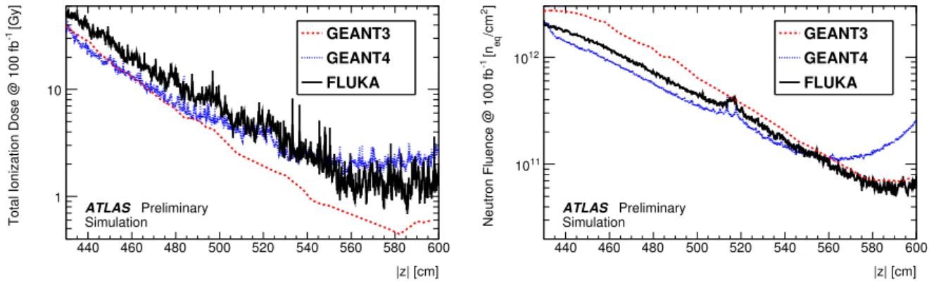
The expected Total Ionization Dose (TID) and 1 MeV neutron fluence (NIEL) in silicon obtained with the three different simulation packages are shown in Figure 1. It can be seen that the FLUKA based simulation predicts a
'30% larger NIEL compared to GEANT4 over most of the
|z|range, with the exception of the region
|z| >550 cm where the missing service parts in the standard ATLAS simulation cause a rise in NIEL, and the front most region with the largest NIEL, where the two simulations agree.
The older GEANT3 based simulation predicts
'50% larger NIEL values for
|z| <500 cm compared to FLUKA and approaches the FLUKA result for larger
|z|. For TID the situation for FLUKA and GEANT4is similar: FLUKA results are up to
'50% above the GEANT4 results for
|z|<500 cm and the GEANT4 predictions rise above the FLUKA predictions for
|z| >550 cm. The GEANT3 predictions are
'50%
lower for TID than those from FLUKA for all
|z|. In general, there is a rather good agreement betweenthe different simulations and a safety factor of 2 on top of the FLUKA predictions can account for all observed variations.
|z| [cm]
440 460 480 500 520 540 560 580 600
[Gy]-1Total Ionization Dose @ 100 fb
1 10
GEANT3 GEANT4 FLUKA
ATLAS Preliminary Simulation
|z| [cm]
440 460 480 500 520 540 560 580 600
]2/cmeq [n-1Neutron Fluence @ 100 fb
1011
1012
GEANT3 GEANT4 FLUKA
ATLAS Preliminary Simulation
Figure 1: Expected radiation levels for TID (left) and NIEL (right) in silicon at the location of the HEC cold electronics for three different simulations. The values correspond to one standard LHC year at √
s=14 TeV with an integrated luminosity of 100 fb−1and without any safety factors applied. The red curve shows the older GEANT3 results, while the blue and black curve show more recent GEANT4 and FLUKA results, respectively.
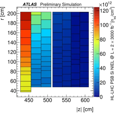
For integrated luminosities of 3000 fb
−1a maximum of 3.1 kGy of total ionization dose (TID) in silicon
are expected from FLUKA, including the safety factor of 2, while the corresponding number for the
1 MeV equivalent neutron fluence (NIEL) in silicon is 1.2
×10
14n
eq/cm2. Figure 2 shows the expected
ATLAS Si-NIEL fluences induced in the ASICs as a function of the location of the read-out cell in the
HEC detector which will be read out by the corresponding ASIC.
|z| [cm]
450 500 550 600
r [cm]
40 60 80 100 120 140 160 180 200
]2 /cm eq [n-1 3000 fb×HL-LHC PSB Si NIEL @ L = 2
0 20 40 60 80 100 120 10
12 ATLAS Preliminary Simulation×
Figure 2: Silicon NIEL fluence in ATLAS under HL-LHC conditions after 3000 fb−1 and with an applied safety factor of 2 to account for simulation uncertainties. The color coded fluences in the Pre-amplification and Summing Boards (PSB) carrying the ASICs are shown at ther−zlocations of the regions in the HEC they read out. The front- most vertical section corresponds to the first read-out layer while adjacent pairs of vertical sections are summed for the three remaining read-out layers. Blocks belonging to the same read-out channel are therefore shown with the same fluence.
3 Irradiation Tests
Proton and neutron irradiation tests have been performed to evaluate the limits of the current read-out electronics under HL-LHC conditions [15].
In addition to the in situ measurements during the irradiation which took place at room temperature, the neutron irradiated boards were re-tested three months after the neutron tests, immersed in liquid nitrogen to simulate the conditions inside the ATLAS endcap cryostat where the read-out electronics of the HEC are located.
3.1 Proton Tests
A 198.9 MeV proton beam of 2.71 nA at the Proton Irradiation Facility (PIF) at PSI, Switzerland with a
narrow beam profile of
σx '7 mm and
σy '9 mm at the position of the devices under test was used in
2011 to evaluate the radiation hardness against hadrons up to a fluence of 2.6
×10
14p/cm
2after 22.05 h
of beam time. A mount with 14 equidistant slots with a slot spacing of 1.7 cm were placed in the beam
line. The six boards closest to the beam window housed transistors in SiGe bipolar and Si CMOS FET
technology and the GaAs FET based ASICs (BB96) [16]. The BB96 ASICs are currently used in ATLAS
for the HEC read-out. Slots 7 and 14 were equipped with radiation diodes for dose measurements, and
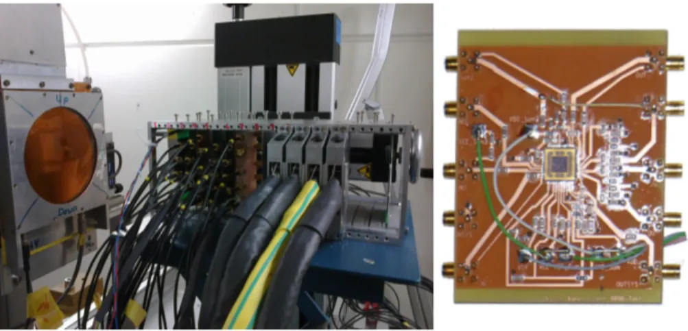
slots 8− 13 with test structures for the HEC power supplies. A picture of the setup prior to final alignment is shown in Figure 3.
Figure 3: Picture of the test setup at PSI prior to final positioning (left). The proton beam comes from the left. An ionization chamber is visible as a large aluminum square with a round hole on the left hand side. The test boards for the HEC read-out electronics (right) are mounted in the first 6 slots of the aluminum frame in the picture center.
The beam position and width were measured with sheets of EBT2 radiation film [17] placed for 5 minutes in the beam behind 6 di
fferent slots. The total beam flux was measured and calibrated by the PIF group with ionization chambers. The raw ionization chamber current measurements in 1 s intervals and the conversion factor to the proton beam current were used to calculate the accumulated proton charge as a function of time. Together with the beam width and position measurements from the radiation films the fluence for the devices under test in each slot was derived. The alignment of the setup was done prior to irradiation by means of two lasers indicating the horizontal and vertical planes containing the beam direction. The laser system was however misaligned for the horizontal plane which led to an o
ffset of (6.5
±0.5) mm in
y, while the positioning of the boards themselves limited the precision in xto about
±
1 mm. Taking into account the small variations of the beam profile along the beam line, the offset of the beam in
y, and the expected losses due to nuclear reactions in the devices under test, the flux was foundto be the same for all slots.
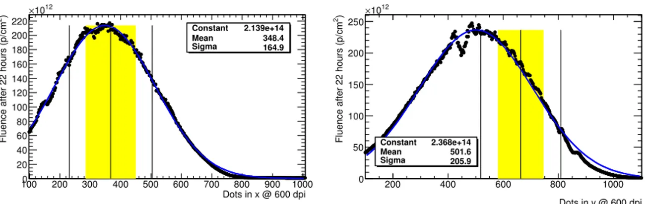
Figure 4 shows the horizontal and vertical profiles of the proton beam as measured by one of the radiation films. Dips in the data distribution are caused by the soldered legs of housings in the upstream slots.
The superimposed Gaussian fits in all films show that the profiles are roughly Gaussian in the area of the ASICs.
3.2 Neutron Tests
Neutron tests were performed in 2012 with a 12
−14
µA and 36 MeV proton beam of the variable-energycyclotron U-120 at NPI in ˇ Rež, Czech Republic, hitting a 16 mm thick D
2O target to produce a neutron
spectrum with
Ekin <32 MeV and
hEkini '14 MeV [18]. Similar to the setup in the proton test, 16
equidistant slots with distances of 1.7 cm between adjacent board centers were equipped and placed in
front of the 3 mm steel plate enclosing the target. The alignment was done prior to mounting the target and
the test boards by burning small holes with the proton beam in two calibration boards placed instead of
the test structures in the first and last slot. Slots 1–6, 8, and 9 were equipped with the BB96 GaAs ASICs,
Constant 2.139e+14 Mean 348.4 Sigma 164.9
Dots in x @ 600 dpi 100 200 300 400 500 600 700 800 900 1000 )2Fluence after 22 hours (p/cm
0 20 40 60 80 100 120 140 160 180 200 220
1012
×
Constant 2.139e+14 Mean 348.4 Sigma 164.9 Constant 2.139e+14 Mean 348.4 Sigma 164.9
Constant 2.368e+14 Mean 501.6 Sigma 205.9
Dots in y @ 600 dpi
200 400 600 800 1000
)2Fluence after 22 hours (p/cm
0 50 100 150 200 250
1012
×
Constant 2.368e+14 Mean 501.6 Sigma 205.9 Constant 2.368e+14 Mean 501.6 Sigma 205.9
Figure 4: Horizontal (left) and vertical (right) profiles of the proton beam at PIF behind slot 3, normalized to the total fluence after 22 hours of beam time. The data points indicate the measurements from the radiation film.
Superimposed are Gaussian fits. The yellow bands depict the position of the ASIC and the vertical lines the center and boundaries of the housing. The film was scanned with a resolution of 600 dots per inch (dpi). The Gaussian parameters for mean and width are also given in dpi.
slots 7 and 11 with radiation diodes and activation foils and the remaining slots with test structures for the HEC power supplies. The setup is shown in Figure 5.
Figure 5: Picture of the test setup at NPI. The neutrons leave the D2O target at the upper left part of the picture and travel to the right. The test boards for the HEC read-out electronics occupy the first 6 slots and slots 8 and 9 of the aluminum frame in the picture center.
The total collected proton charge in the test was 2.0 C. The neutron flux profile was measured with sheets of EBT2 radiation film placed for 5 minutes at a reduced machine current of 1.2
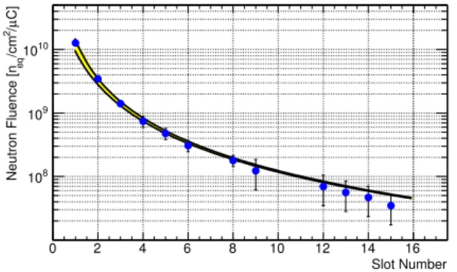
µA in front of slot 1 andbehind all other slots with the exception of slots 7,10, and 11. During a dedicated fluence test run in 2010 with radiation monitors in each slot the following empirical relation of the 1 MeV equivalent neutron fluence in silicon and the integrated machine current as function of the slot number was found [19]:
fluence
=1.61
×10
10n
eqcm
2µCslot
+o
ffset
±2 mm 17 mm
!−2.11
,
(1)
where slot is the slot-number (1-16), o
ffset is the distance of the first slot from the target (3 mm) and the positions are known with
±2 mm precision.Slot Number
0 2 4 6 8 10 12 14 16
C]µ/2/cmeqNeutron Fluence [n 810
109
1010
Figure 6: 1 MeV equivalent neutron fluence in silicon as function of slot number normalized to the integrated machine current. The data points depict relative dose measurements from radiation films normalized to the expected fluence in slot 3. The band between the two solid lines corresponds to the fluence curve measured in 2010 in a dedicated run with radiation monitors in each slot.
Figure 6 shows this fluence curve superimposed with the relative fluence measurements from the radiation films, normalized to the expected fluence in slot 3.
3.3 S-Parameter Measurements
During the irradiation the scattering parameters (S-parameters) [20] of the BB96 ASICs were continu- ously measured to study their performance as a function of fluence. S-parameters describe the electrical behavior of a linear electrical network in the frequency domain. The S-parameters were measured for the frequency range 300 kHz to 100 MHz with a vector network analyzer (VNA) connected via 40 m long cables to the devices under test. Each cable pair was individually de-embedded with the VNA calibration utility [21] moving the plane of calibration to the input connectors of the boards. The most important parameters are the input port reflection coe
fficient
S11, which can be translated into the input impedance
Zin=50
Ω(1
+S11)/(1
−S11) for the case of vanishing feedback coe
fficient
S12and low load reflection, and the forward transmission coefficient
S21. The product of the two gives the transimpedance gain in the frequency domain. This can be interpreted as the input current to output voltage signal amplification. It was found that the e
ffect of protons in the GaAs ASICs is similar to that of neutrons with
∼5 times largerfluence. Since the expected ratio of neutron to proton fluence for the HL-LHC is
∼10 [1], the neutron tests provide the most limiting numbers.
3.4 Pulse Measurements
In the neutron test triangular voltage pulses similar to the ionization currents in the LAr gaps in ATLAS
with 10 different amplitudes between 0.7 mV and 70 mV and pulse lengths of 500 ns were applied over
the 40 m cables at the BB96 ASICs, and both the input and the output pulse were measured with an
oscilloscope (the output pulse again after a 40 m cable). These measurements were done alternatingly
with the S-parameter measurements and provide a more direct way of studying the performance of the
electronics. Good agreement with the S-parameter measurements was found for the gain as a function of
neutron fluence. The largest expected ionization currents in ATLAS are 250
µA for a single pre-amplifier(PA) and about 500
µA for a full chain of several PAs and one summing amplifier or driver. Up to thesevalues the linearity of the PAs and the full system was measured with pulses. To convert from input voltage pulses to currents the input impedance and cable damping was taken into account. The voltage range of 0.7 mV to 70 mV corresponds to an input current range of 10
µA to 1000µA for non-irradiatedchips.
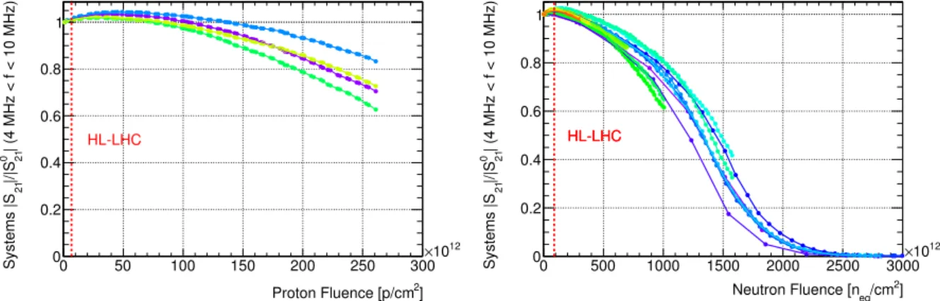
3.5 Warm in Situ Results
The forward transmission coefficient normalized to the value before irradiation and evaluated in the fre- quency range of the shaper electronics in ATLAS (4 MHz
< f <10 MHz) as measured in situ for the full systems consisting of one PA and a summing amplifier during the proton and neutron irradiations is shown in Figure 7 as function of the proton and 1 MeV equivalent neutron fluence in silicon. Figure 7
2] Proton Fluence [p/cm
0 50 100 150 200 250 300
1012
×
| (4 MHz < f < 10 MHz)0 21|/|S21Systems |S 0
0.2 0.4 0.6 0.8 1
HL-LHC
2]
eq/cm Neutron Fluence [n
0 500 1000 1500 2000 2500 3000
1012
×
| (4 MHz < f < 10 MHz)0 21|/|S 21Systems |S 0
0.2 0.4 0.6 0.8 1
HL-LHC HL-LHC
Figure 7: Forward transmission coefficient normalized to the value before irradiation and evaluated in the frequency range of the shaper electronics in ATLAS (4 MHz < f < 10 MHz) as measured in situ for a system of PA and summing amplifier during the proton (left) and neutron (right) irradiations versus the fluence. The neutron fluence is given in 1 MeV equivalent for silicon as measured in ˇRež. The red vertical lines indicate HL-LHC limits including a safety factor of 2. In the proton case the limit assumes all damage would be due to TID of the protons (neglecting NIEL). In the neutron case the fluence limit is corrected by the expected differences in GaAs (see Section3.7). The colored data points are from the various devices under test and the spread of the points indicate sample variations.
Since for the neutron test the fluence varied with slot number the point density and maximal fluence per slot varies.
shows that the device-to-device fluctuations increase with irradiation and that the e
ffect of protons is about 4
−5 times larger on the voltage gain compared to that of neutrons at the same fluence values. Input im- pedances were found to stay close to 50
Ωand are real throughout the entire irradiation range for protons and up to
∼4×10
14n
eq/cm2for neutrons. The output impedance shows similar behavior and stays close to 50
Ωroughly twice as long. Beyond these limits the impedances stay real but rise quickly resulting in non-matched conditions in ATLAS, where 0.5
−2 m 50
Ωcables connect the detector and the PAs and
∼10 m 50Ω
cables carry the signals from the ASIC output to the shaper electronics.
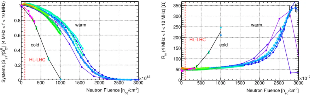
3.6 Cold Results
About three months after the neutron irradiation tests at NPI in ˇ Rež the irradiated boards were shipped
to the MPP lab in Munich and re-tested with the same set of measurements as in situ in both warm and
cold (liquid nitrogen) conditions. The three front-most boards received neutron fluences in excess of 2.8
×10
15n
eq/cm2(Si 1 MeV eq. in ˇ Rež). From Figure 7 it can be seen that beyond 2.1
×10
15n
eq/cm2the ASICs approach 0 voltage gain and therefore the three first boards were not functioning anymore. The board in the fourth slot was exposed to 1.6×10
15n
eq/cm2and this one plus the following four boards from slots 5,6,8, and 9, with respective fluences of 10.0, 6.9, 3.8, and 3.0
×10
14n
eq/cm2were still operational in warm conditions and still showed the same performance as was measured at the end of the run in situ at ˇ Rež. In addition to these 5 fluence points non-irradiated ASICs have been measured in warm and cold as well to provide data at zero fluence. Immersed in liquid nitrogen to emulate the conditions inside
2]
eq/cm Neutron Fluence [n
0 500 1000 1500 2000 2500 3000
1012
×
| (4 MHz < f < 10 MHz)0 21|/|S21Systems |S 0
0.2 0.4 0.6 0.8 1
warm
cold
HL-LHC
2]
eq/cm Neutron Fluence [n
0 500 1000 1500 2000 2500 3000
1012
× ]Ω (4 MHz < f < 10 MHz) [inR
0 50 100 150 200 250 300 350
warm
cold HL-LHC
Figure 8: Forward transmission coefficient normalized to the value before irradiation (left) and input impedance (right) evaluated in the frequency range of the shaper electronics in ATLAS (4 MHz< f <10 MHz) as measured in situ for systems of a PA and a summing amplifier during the neutron irradiations in warm and in cold three months after the irradiation versus the fluence. The neutron fluence is given in 1 MeV equivalent for silicon. The red vertical lines indicate the HL-LHC limit including a safety factor of 2.
the ATLAS cryostat, the performance is dramatically worse than in warm conditions. Figure 8 shows the normalized forward transmission coe
fficient and the input impedance for the systems comprised of one PA and a summing amplifier as function of neutron fluence for both warm and cold conditions. The sparse data points on the left indicate the cold measurements, while the denser groups of points extending to larger fluences are the measurements in warm. The performance in cold is roughly equivalent to that in warm at 3 times larger fluences. The performance degrades quickly beyond 3
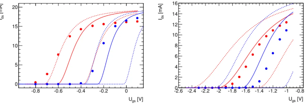
−4
×10
14n
eq/cm2. In order to understand the large temperature dependence in performance degradation for the BB96 ASIC the DC characteristics of the two types of transistors used in the ASIC (so called DFET and MFET) have been tested at room temperature and immersed in liquid nitrogen. Figure 9 shows these measurements compared to SPICE-simulations for the transistors. While the model parameter variations (indicated by the dashed lines) allow for a wide range of possible IV-curves, the measured and predicted curves show the same shift in threshold voltage by
∆Vth '+0.4 V for both transistor types in the transition of warm tocold conditions.
In Figure 10 the threshold voltage
Vthfor both transistor types is shown as measured in situ (warm) during neutron irradiations at ˇ Rež. For a Si-NIEL fluence of 1
·10
15n
eq/cm2threshold voltage increases of 0.45 V (DFET) and 0.60 V (MFET) are observed, respectively. It can be concluded that the operation in cold has the same effect on the transistors as irradiating them with 6
−8
·10
14n
eq/cm2. The same offset of 6
−8
·10
14n
eq/cm2can be observed in Figure 8 when warm and cold values for the forward transmission coe
fficient are compared.
The pulse measurements as described in Section 3.4 have also been repeated with the already irradiated
gs [V]
U
-0.8 -0.6 -0.4 -0.2 0
[mA]dsI
0 5 10 15 20
gs [V]
U -2.6 -2.4 -2.2 -2 -1.8 -1.6 -1.4 -1.2 -1 -0.8 [mA]dsI
0 2 4 6 8 10 12 14 16
Figure 9: Drain-Source current of DFET (left) and MFET (right) transistors in warm (red) and cold (blue) versus the Gate-Source voltage for a small applied Drain-Source voltage (10 mV). The solid dots show measured data; solid lines are model predictions for default model parameters; dashed lines correspond to variations in the model para- meters.
2]
eq/cm Neutron Fluence [n
0 200 400 600 800 1000
1012
× [V]thV
-0.8 -0.7 -0.6 -0.5 -0.4 -0.3
( 1.22e-15 * Fl + 1 ) = -0.80 V + 1.32 V * log10
Vth
2]
eq/cm Neutron Fluence [n
0 200 400 600 800 1000
1012
× [V]thV
-1.9 -1.8 -1.7 -1.6 -1.5 -1.4 -1.3 -1.2
( 1.58e-15 * Fl + 1 ) = -1.87 V + 1.51 V * log10
Vth ( 1.58e-15 * Fl + 1 )
= -1.87 V + 1.51 V * log10
Vth
Figure 10: Threshold voltageVth of DFET (left) and MFET (right) transistors in warm under neutron irradiation versus the neutron fluence. The solid dots show measured data; solid lines indicate a fit to a logarithmic function.
The apparent fluctuations for the MFET around threshold voltages of−1.4 V are due to the small number of working points (step size 0.05 V) available during the measurements.
boards in warm and in cold. The pulse amplitudes have been adjusted to lower levels to still correspond to 10
−1000
µA input currents for non-irradiated ASICs for the short (∼4 m) cables used at MPP. Theincrease of non-linearity of the response was found to be described by a power-law relation of input (in) and output (out) amplitude of the form:
out
=c×in
x,(2)
where
cis a fluence-dependent constant and
xthe power-law exponent. Values for
xdeviating from 1.0 indicate non-linear behavior.
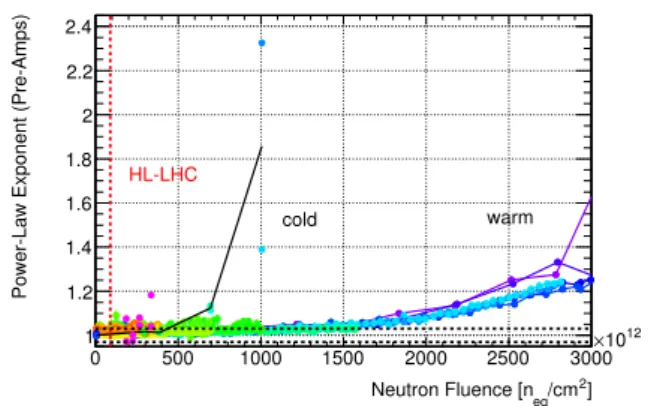
Figure 11 shows this exponent as function of neutron fluence in warm and cold. As in the case of the
forward transmission coefficient the non-linearities for irradiated ASICs are worse in cold and correspond
roughly to those in warm at 3 times larger fluences. Since up to 16 PAs are summed by one summing
2]
eq/cm Neutron Fluence [n
0 500 1000 1500 2000 2500 3000
1012
×
Power-Law Exponent (Pre-Amps)
1 1.2 1.4 1.6 1.8 2 2.2 2.4
cold warm HL-LHC
Figure 11: Measured non-linearity of the PAs as function of neutron fluence in warm (dense data points extending to large fluences) and in cold (sparse data points at lower fluences). The non-linearity is expressed in terms of a power-law exponent. Deviations from 1.0 indicate non-linear behavior. Horizontal dashed lines indicate exponent limits for a deviation of 1% from linear expectation of the output amplitude normalized to the maximum amplitude.
The neutron fluence is given in 1 MeV equivalent for silicon. The red vertical line indicates the HL-LHC limit including a safety factor of 2.
amplifier in ATLAS the non-linearities for the PAs can not be corrected. An exponent of 1.03 or 0.97 would correspond to a maximum deviation of 1% of the output amplitude normalized to the maximum amplitude from linear expectation. This original requirement limit for the non-linearity of the PAs is indicated by the horizontal lines in Figure 11. Beyond neutron fluences of 3
−4
×10
14n
eq/cm2the non-linearity quickly rises above this level.
! "#!
"$%!&'()*+, -./0!
01$&'&
-$2&3*44
!5.60 % 705 889)
-./0%
01$&'&
-$:(33*44 ;10<=>+01!
7!$&33*?=4
@+$) <=>+01!
7A0#@>./!
7$23*?=4 /
B.C=@>./?DE A0#@>./?DE -FG@>./?DE
Figure 12: The full electronics chain for a typical HEC channel with detector capacitanceCd = 213.76 pF and a 530 mm coax cable between detector and ASIC. The ASIC (BB96 in the figure) is described by the measured S- parameters. The output is connected via a∼8.7 m coax cable to pre-shaper and shaper circuits. The typical medium gain amplification of the shaper is assumed.
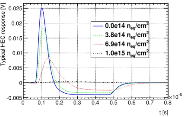
The degraded S-parameter measurements in cold over the full frequency range of 300 kHz
−100 MHz
have been used to predict the response to a typical ionization signal in the HEC after the full electronics
chain for the HEC in ATLAS [22] (see Figure 12). Figure 13 shows the simulated response to a 400 ns
triangular current in a typical HEC channel at four di
fferent fluence values. It can be seen that on top
of the gain degradation the pulse shape worsens with increasing fluence leading to a slower rise- and
fall-time, a broader and more delayed positive peak.
t [s]
0 0.1 0.2 0.3 0.4 0.5 0.6 0.7 0.8
10-6
×
Typical HEC response [V]
-0.005 0 0.005 0.01 0.015 0.02 0.025
/cm2
0.0e14 neq
/cm2
3.8e14 neq
/cm2
6.9e14 neq
/cm2
1.0e15 neq
Figure 13: Simulated typical response in cold to a 400 ns triangular ionization current in the HEC for one channel for four different neutron fluences. The fluence is given as 1 MeV equivalent fluence in silicon for the neutron spectrum at NPI in ˇRež.
3.7 Fluence Conversion for GaAs
The neutron fluence values given in all figures presented so far (if not explicitly stated otherwise like in Figure 2) are 1 MeV equivalent fluences in silicon evaluated for the neutron spectrum at NPI in ˇ Rež [18].
In order to compare these values to expectations for the HL-LHC the fluences have to be converted for the GaAs devices studied here first to the corresponding 1 MeV equivalent fluence in GaAs using the NPI neutron spectrum and the Kerma factors for neutrons in silicon and gallium-arsenide [23–29]. In a second step, using the expected neutron, proton and pion spectra in ATLAS [12], the 1 MeV equivalent neutron fluence in GaAs has to be converted back to Si using Kerma factors for the relevant radiation in both Si and GaAs. It was found that the conversion from Si to GaAs at NPI energies is 1.82 and from GaAs to Si at the location of the ASICs in ATLAS 1/1.35. All measured neutron fluences at NPI reported here can thus be converted to ATLAS expectations by multiplying with 1.82/1.35.
4 BB96 Ageing Tests
Another aspect of the qualification of the HEC cold electronics for operation under HL-LHC conditions is the investigation of potential ageing effects on their performance. At the end of the HL-LHC operation, the BB96 ASICs will have been in operation under radiation for over 20 years. Since robust data about the long-term stability of electronic components in these conditions is not available, an e
ffort was under- taken to accelerate the ageing process in the lab, and then look for performance degradation and signs of mechanical stress or damage of the electronic components.
4.1 Cold Ageing Test
The HEC read-out electronics are immersed in liquid argon inside the HEC cryostat and operating at
87K. To study ageing at cryogenic temperatures, four PCBs, each equipped with 2 pre-amplifiers and
2 sytems, were kept unpowered for 16 days inside a cryostat filled with liquid nitrogen, and various
performance parameters of the ASICs were measured before and after the test: DC-values, S-parameters
Table 1: Relative performance degradation of BB96 ASICs after≈16 days (386 hours) at -190◦ (unpowered).∆|S21| denotes the relative change in the forward transmission coefficient and∆Rin(out)the relative changes in the real parts of input and output impedance, respectively.
ASIC Correction for
∆|S21|(%)
∆Rin(%)
∆Rout(%) temperature only -1.1
±0.4 1.5
±0.5 0.2
±0.1 Pre-Amps temperature and light -0.9
±0.4 1.2
±0.5 0.1
±0.1 light only -1.1
±0.4 1.7
±0.4 0.1
±0.1 temperature only -0.8
±0.4 1.6
±0.6 0.4
±0.3 Systems temperature and light -0.7
±0.4 1.2
±0.6 0.3
±0.3 light only -1.0
±0.4 1.7
±0.5 0.4
±0.3
(see Section 3.3), and the pulse response as described in Section 3.4. The left-hand side of Figure 14 shows a picture of the PCBs inside the cryostat.
DUT
202 204 206 208 210 212 214 216
|21|S
0.78 0.8 0.82 0.84 0.86
0.4) %
±
| = (0.9
|S21
∆
before cold test after cold test
after cold test, temperature-corrected additional correction for light exposure
Figure 14: A picture of the four PCBs inside the cryostat (left), and a comparison of|S21|for all pre-amplifiers before and after the cold test, with several corrections applied (right). The abscissa indicates the number of the device under test (DUT).
Some minor differences between the measurements before and after the cold test complicate their com-
parison: there was a temperature difference between the two measurements ranging from
∆T = +0.70◦to
∆T = +1.85
◦, depending on the specific PCB; the chips were covered with a plastic lid before the test
which was removed before putting them inside the cryostat; and after the cold test, a few channels were
not working because of problems in the outer circuitry. To correct for these differences, some additional
un-irradiated PCBs were used to study their temperature dependence and their response to light exposure,
and an example of applying the resulting correction factors to the measurements is shown in the right-
hand side of Figure 14 for
|S21|of the pre-amplifiers. The results of the cold ageing test are reported in
Table 1, with the various correction schemes yielding similar results. In summary, a small performance
degradation of the order of 1% is observed after 16 days in liquid nitrogen. It is clear that this 1% de-
gradation over a period of 16 days cannot simply be linearly extrapolated to longer time scales, since the
BB96 ASICs currently in operation in the ATLAS detector do not show any degradation that would be
compatible with such an assumption. The result is thus attributed either to an initial drop in performance
after cooling down the ASICs or to some unknown systematic effect of the measurements.
Table 2: Relative performance degradation of BB96 ASICs after 86 temperature cycles between 5◦C and 100◦C (unpowered). The parameter definitions are the same as in Table1.
ASIC
∆|S21|(%)
∆Rin(%)
∆Rout(%) Pre-Amps -0.3
±0.5 0.5
±0.6 0.0
±0.1
Systems -0.2
±0.1 1.0
±1.5 0.0
±0.2
4.2 Warm Ageing Test
Another way to artificially accelerate the ageing process of electronic devices is to temperature-cycle them. A different set of four PCBs were exposed to 86 temperature cycles between
+5◦C and
+100◦C over a period of 14 days with each stage of constant or ramping temperature lasting for about an hour.
The right-hand plot of Figure 15 compares the measurements of
|S21|for the pre-amplifiers with the data taken prior to the temperature cycles (warm test). These comparisons are also shown in numerical form in Table 2. The results for all parameters are compatible with the observation of no performance degradation.
DUT
218 220 222 224 226 228 230 232
|21|S
0.66 0.68 0.7 0.72 0.74 0.76 0.78 0.8 0.82 0.84
0.5) %
±
| = (-0.3
|S21
∆
before warm test after warm test
Figure 15: An electron microscope picture of one die packaged without lid onto a PCB, taken after the warm test (left), and a comparison of|S21|for all pre-amplifiers (DUT) before and after the warm test (right).
In addition to evaluating performance parameters, individual transistors were examined for signs of mech-
anical stress or damage after the warm test with both optical and electron microscopes. The electron
microscope examination was performed at the ScopeM facility at the ETH Zürich, and the left-hand side
of Figure 15 shows an example of the many electron microscope pictures that were taken. No signs of
mechanical damage were visible after either the cold or the warm test. The material analysis performed
supplementarily at ETH confirmed the material composition of the dies and was useful to exclude poten-
tial ageing problems from Al-Au junctions or inappropriate glue.
5 Impact of Degraded Electronics on ATLAS
The extrapolation of the performance of the read-out electronics shown in Figure 13 and described in Section 3.6 can be extended to other fluence values. The S-parameters have been interpolated between the measured values and parameterized as function of the fluence. The interpolated data sets have been used to predict the pulse shapes for these fluence values in different HEC read-out cells. For a typical HEC read-out cell the resulting pulse from the interpolation of S-parameters as function of time for various ATLAS Si-NIEL fluences in steps of 1.0
×10
14n
eq/cm2is shown in the left plot of Figure 16.
The right plot in the same figure shows the autocorrelation function – the folded response to a delta-peak with itself – normalized to unit amplitude as function of the sample number (one sample is taken every 25 ns in ATLAS) for the same fluence values. The e
ffective gain for an ionization signal is determined from the pulse amplitudes, but the full signal reconstruction in ATLAS uses the autocorrelation functions to calculate optimal filter weights in the digitization step. This is done in the simulation described in the next sections. Also the actual electronics noise could be simulated with the autocorrelation function but in ATLAS is taken from measured noise data instead – so the increase in noise due to degraded pulse shapes is not fully accounted for.
t [s]
0 0.1 0.2 0.3 0.4 0.5 0.6 0.7 0.8
10-6
×
Typical HEC response [V]
-0.005 0 0.005 0.01 0.015 0.02
0.025 ATLAS Si-NIEL Layer 0 Region 0 Eta 1 /cm2 0.0e14 neq
/cm2 1.0e14 neq
/cm2 2.0e14 neq
/cm2 3.0e14 neq
/cm2 4.0e14 neq
/cm2 5.0e14 neq
/cm2 6.0e14 neq
/cm2 7.0e14 neq
/cm2 8.0e14 neq
/cm2 9.0e14 neq
/cm2 10.0e14 neq
/cm2 11.0e14 neq
/cm2 12.0e14 neq
/cm2 13.0e14 neq
Sample Number
0 5 10 15 20 25 30
Autocorrelation
-0.4 -0.2 0 0.2 0.4 0.6 0.8
1 ATLAS Si-NIEL Layer 0 Region 0 Eta 1
/cm2 0.0e14 neq
/cm2 1.0e14 neq
/cm2 2.0e14 neq
/cm2 3.0e14 neq
/cm2 4.0e14 neq
/cm2 5.0e14 neq
/cm2 6.0e14 neq
/cm2 7.0e14 neq
/cm2 8.0e14 neq
/cm2 9.0e14 neq
/cm2 10.0e14 neq
/cm2 11.0e14 neq
/cm2 12.0e14 neq
/cm2 13.0e14 neq
Figure 16: Simulated typical response (left) to a 400 ns triangular ionization current in the HEC and the correspond- ing autocorrelation function (right) for one channel for different NIEL fluences for silicon in ATLAS.
The increase of the non-linearity exponent
xunder irradiation can be modeled with a simple function of the form:
x= x0+
exp(c
0+c1×Fl),(3)
where
x0,
c0, and
c1are constants and
Flis the Si-NIEL fluence as measured in ˇ Rež. Figure 17 shows the exponent fit to the measured data points as function of Si-NIEL in ˇ Rež for the PAs alone (top left) and the systems (PA and driver) (top right). The bottom plot in the same figure shows the two fit functions compared to their ratio, which can be interpreted as the non-linearity of the driver stage alone. From the ratio it can be seen that most of the non-linear behavior stems from the pre-amplification, not the driver.
The fitted values of the non-linearity exponent for the PAs are:
x0 =
1 (fixed);
c0=−5.64
±0.63;
c1=(5.46
±0.91)
×10
−15cm
2/neq.(4)
2]
eq/cm Neutron Fluence [n
0 200 400 600 800 1000 1200
1012
×
Power-Law Exponent (Pre-Amps)
1 1.2 1.4 1.6 1.8 2 2.2 2.4
2)) eq/cm 1+exp(-5.64 + 5.46e-15*Fl/(n
HL-LHC
2]
eq/cm Neutron Fluence [n
0 200 400 600 800 1000 1200
1012
×
Power-Law Exponent (Systems)
1 1.2 1.4 1.6 1.8 2 2.2 2.4
2)) eq/cm 1+exp(-4.37 + 4.38e-15*Fl/(n
HL-LHC
2]
eq/cm Neutron Fluence [n
0 200 400 600 800 1000 1200
1012
×
Power-Law Exponent
1 1.5 2 2.5 3 3.5
Systems Pre-Amps
Driver = Systems/Pre-Amps
HL-LHC
Figure 17: Non-linearity of the PAs as function of neutron fluence in cold for the PAs (top left) and the systems consisting of PA and driver (top right). Superimposed are fits to the data (constant plus exponential as in Eq.3).
Both fits and their ratio are shown in the bottom plot. The ratio can be interpreted as the non-linearity stemming from the driver stage. Thus the main contribution to the non-linearity originates in the PAs.
5.1 Parameterization of Degradation
A di-jet Monte Carlo sample was chosen to study the HEC performance degradation due to radiation damage. The PYTHIA [30] Monte Carlo generator was used to generate hard scattering 2→2 QCD processes with two leading jets in the intermediate
pT-range (140 GeV
< pT <280 GeV), overlapping at least partially with the HEC region (1.5
< |η| <3.2). ATLAS uses anti-k
Tjets [31] with a distance parameter of
R=0.4 and thus the simulated
ηrange to partially overlap with the HEC was chosen to be 1.1
<|η|<3.6. A total of 16300 di-jet events have been generated and fully simulated [9]. The simulated sample does not include any pile-up of pp collisions.
A dedicated event sample produced at the initial stage of the simulation (prior to the digitization and reconstruction procedures) contains the values of energy deposited in each HEC sub-gap in a given event.
If no degradation is assumed, these initial values remain unchanged and enter the digitization and recon- struction procedures. The degradation of electronics is taken into account by replacing the initial energy values with re-calculated, distorted values, such that the reconstructed jet energy contains the footprints of the HEC electronics radiation damages, as explained below.
For each of four layers of the HEC, an average value of the expected neutron fluence has been used as presented in Figure 2. The actual value of the gain degradation factor,
gi, assigned to individual PAs in the PSB layer was randomly selected using a Gaussian function with parameters as presented in Table 3.
The degraded measurement of the energy in each HEC sub-gap was calculated as
E0 = Einit·gi. The PA
Table 3: Average values of the HEC electronics degradation parameters.
PSB n-fluence gain decrease non-linearity layer [n
eq/cm2] factor,
gexponent,
p0 1.2·10
140.953±0.008 1.006±0.001 1 7.1·10
130.972±0.005 1.005±0.001 2 1.3·10
130.995±0.002 1.004±0.001 3 3.8·10
120.998±0.001 1.004±0.001
output signals are summed actively by the summing stage of the ASIC and an overall calibration factor can be applied to the summed output. For a group of typically four summed PAs one correction coefficient
Cg=4/(g
1+g2+g3+g4) was determined and applied to each of the four PAs individually, such that that
E00= E0·Cg.
The signal non-linearity cannot be corrected by means of the HEC calibration system. A dedicated o
ff-line method may however be developed in future to reduce the e
ffect, but since typically four PAs are summed and only the summed signal can be corrected it is not possible to fully account for the degradation introduced by non-linearities.
The non-linearity e
ffect was introduced in the simulation by taking into account the measured increase of the power-law exponent with the increase of radiation dose. The average values of selected degradation parameters are shown in Table 3. Again, a randomly selected non-linearity factor,
p, was assigned to eachPA and a new value of the deposited energy was calculated as
Edegr =(E
00)
pE(1−p)ref, where
Erefdenotes a renormalization energy scale in order to equalize the visible energy before and after the degradation at the selected energy point. The choice of this reference scale is a bit arbitrary but should be in the range of typical energies measured in ATLAS for which it is assumed that the calibration factors restore the correct energy on average. In the analysis, the reference energy is once set to 100 GeV for all HEC layers and once to 5 GeV and 10 GeV, to account for different sampling fractions in front and rear longitudinal sections of the HEC, respectively.
Finally, the initial values of the deposited energy in every HEC sub-gap,
Einit, were replaced in each event by the degraded values,
Edegr, and the regular digitization and reconstruction algorithms were applied.
The degraded pulse shape and autocorrelation functions corresponding to the assumed fluence values for each individual HEC channel were used in the digitization step instead of the default ATLAS values.
5.2 Simulation Results
Figure 18 shows results of the Monte-Carlo simulation for spectra of visible energy deposited in the LAr gaps and recorded in the front longitudinal HEC layer. The initial distribution (corresponding to
Einit) is shown by black dots, whereas the histograms show results of the degradation algorithm applications, and the quoted numbers represent the average and RMS values of the corresponding distributions, re- spectively. The solid red line shows the visible energy spectrum obtained when considering gain and pulse shape degradation only (corresponding to
E00– i.e. corrected for the expected average gain loss).
The comparison to the initial distribution shows that the calibration procedure can almost recover the
Visible deposited energy in LAr gap in HEC front layer [GeV]
0 1 2 3 4 5 6 7 8 9 10
# entries
1 10 102
103
104
105
106
107
Mean/GeV RMS/GeV Initial 0.00449 0.03667 gain loss only 0.00445 0.03635 norm 100 GeV 0.00427 0.03541 comb 5 & 10 GeV 0.00434 0.03601
ATLAS Preliminary Simulation
Figure 18: Distribution of the visible energy deposited in LAr gaps in the front HEC layer. The dots show the initial non-distorted distribution, the red histogram shows the effect of pulse-shape and gain degradation after correcting for the gain loss and the dashed and blue histograms the full degraded results with non-linearities taken into account for two choices of the reference energy scale for normalization.
degradation due to the PA’s gain loss. The two other histograms demonstrate the final energy spectra (cor- responding to
Edegr) with non-linearities taken into account for two different normalizations performed at 100 GeV (dashed line) and at 5 and 10 GeV (blue solid line) for the front and rear longitudinal HEC segments, respectively. As expected, the normalization at the higher energy point results in lower visible energies, while the combined approach at lower energies provides better results when comparing to the initial distribution. The combined normalization is used from this point on.
The effect of electronics degradation on the HEC performance is very small as can be seen from the results shown in Figure 19. The jet performance plots show standard reconstructed anti-k
Tjets with the distance parameter
R =0.4. The jets are constituted of calibrated topological clusters [32] and jet energy scale corrections [33] are applied. The top left plot in Figure 19 shows the energy distribution for the two leading jets in transverse momentum, reconstructed from the initial and degraded values of the deposited energy. One may note a shift of the degraded jet energy spectrum to lower values (in this case by
∼0.5%).Reconstructed jets were matched in
∆R= ∆η⊕∆φto Monte-Carlo jets at particle level (truth) by requiring
∆R<
0.4. Distributions of the difference of reconstructed and truth jet energies were analysed for various truth jet energy intervals.
The energy dependence of the ratio of the RMS of the reconstructed jet energy over the mean recon-
structed jet energy (jet energy resolution) is shown in Figure 19 (top right), whereas Figure 19 (bottom
right) demonstrates the ratio between the mean reconstructed jet energy and the truth value (linearity) as a
function of truth jet energy. The results are presented for initial and degraded jets. No significant change
of the jet energy resolution is observed while the linearity degrades by
∼0.5%. Also no significant de-
gradation of the HEC performance is seen in Figure 19 (bottom left) where the initial transverse missing
transverse momentum (MissingET) spectrum is compared to the degraded case. Larger deterioration of
HEC PAs would affect the MissingET by introducing a tail with larger MissingET values – but at the
radiation levels studied here this is not yet the case.
Reconstructed jet energy [GeV]
0 500 1000 1500 2000 2500 3000 3500 4000 4500 5000
# events
1 10 102 103
Mean/GeV RMS/GeV
Initial 628.04 410.59 Degraded 624.84 408.76
ATLAS Preliminary Simulation
Monte-Carlo jet energy [GeV]
0 200 400 600 800 1000 1200 1400 1600
Jet energy resolution
0 0.05 0.1 0.15 0.2
Initial Degraded
ATLAS Preliminary Simulation
MissingET [GeV]
0 20 40 60 80 100 120 140
# events
1 10 102 103
Mean/GeV RMS/GeV
Initial 28.60 15.63 Degraded 27.96 15.37
ATLAS Preliminary Simulation
Monte-Carlo jet energy [GeV]
0 200 400 600 800 1000 1200 1400 1600
Jet energy linearity
0.96 0.97 0.98 0.99 1 1.01 1.02
Initial Degraded
ATLAS Preliminary Simulation
Figure 19: Summary of the electronics degradation on HEC performance: reconstructed jet energy spectra for calibrated anti-kT jets with distance parameterR =0.4 (top left); energy dependence of the jet energy resolution (top right) and relative non-linearity (bottom right); missing transverse momentum (MissingET) spectra (bottom left).