Performance of the New Amplifier–Shaper–
Discriminator Chip for the ATLAS MDT Chambers at the HL-LHC
M. De Matteis
a, F. Resta
a, R. Richter
b, H. Kroha
b, M. Fras
b, Y. Zhao
b, V. Danielyan
b, S. Abovyan
b, A. Baschirotto
aaPhysics Department,
Piazza della Scienza 3, Milano, Italy
bMax-Planck-Institute for Physics, Munich, Germany
E-mail: marcello.dematteis@unimib.it
A
BSTRACT: The Phase-II Upgrade of the ATLAS Muon Detector requires new electronics for the readout of the MDT drift tubes. The first processing stage, the Amplifier-Shaper- Discriminator (ASD), determines the performance of the readout for crucial parameters like time resolution, gain uniformity, efficiency and noise rejection. An 8-channel ASD chip, using the IBM 130 nm CMOS 8RF-DM technology, has been designed, produced and tested. The area of the chip is 2.2 x 2.9 mm
2size. We present results of detailed measurements as well as a comparison with simulation results of the chip behavior at three different levels of detail.
K
EYWORDS: ATLAS; Muon-Drift-Tubes; Detector; CMOS Front-End.
– 1 – Contents
1
1. Introduction 1
2
2. The ATLAS Experiment 2
3
3. MDT-ASD Circuital Implementation 3
4
3.1 Charge-Sensitive-Preamplifier 3
5
3.2 DA
1-DA
2-DA
35
6
3.3 Wilkinson A/D 5
7
4. Preliminary Measurements Result 6
8
4.1 8xAFE Electrical Characterization 6
9
5. Conclusions 6
10 11
1. Introduction
12
In the last years Integrated Circuit (IC) solutions have been widely used in High-Energy Physics 13
experiments (HEP). The main aim is to replace common service electronics (based on very old 14
CMOS processes and/or off-the-shelf components [1] [2]) with more efficient scaled-down ICs, 15
in order to improve sensitivity/noise/power performance while reducing area. Consequently, the 16
increased pixels readout resolution automatically leads to better imaging and understanding of 17
the particles collision phenomena.
18
The present Analog Front-End (AFE) [1], installed into the ATLAS experiment Muon Detector, 19
has been developed in Agilent 500 nm technology with 3.3 V of supply voltage. The chip 20
includes eight channels performing up to eight detections at the same time. The signal resulting 21
from a charge-to-voltage conversion is amplified/shaped by an analog chain, and then it is sent 22
to an A/D converter.
23
Despite this ASD has good operation experience in 'edge mode' and very low failure rate, a 24
Detector upgrade (known as CMS Phase 2 ( [2])) is expected in the next years. The HL-LHC at 25
CERN will operate at peak luminosities of a factor 5 - 7.5 beyond the nominal value of 1034 26
cm
-2-1. This high luminosity is a challenge for the MDT readout system for two aspects. Higher 27
hit rates, mainly due to increased cavern background, drive data transmission to the rear end 28
electronics to the limit of available bandwidth. In addition, the new L1 trigger operating 29
parameters - latency up to 0.06 ms and trigger rates up to 400 kHz - call for a replacement of the 30
entire readout chain. The most critical element in the latter is the first stage, i.e. the Amplifier 31
with the Shaper and the Discriminator (ASD). Signal rise-time, signal-to-noise ratio and 32
threshold uniformity among channels are decisive for system parameters like track coordinates 33
spatial resolution and tracking efficiency. To cope with this requirements, a chip has developed 34
in the IBM 130 nm CMOS technology.
35
The technology choice depends on radiation hardness. In fact, the design kit has been used for 36
several CERN ICs showing mature simulation tools with reasonable costs. A move to 65nm 37
technology would have implied a not required scaling-down, together with higher costs and 38
models still under development/debugging.
39
– 2 –
As concerns the 8xAFE design, the first characterizing measurements are here presented. The 40
ASIC contains a preamplifier, three shaping stages and a discriminator. In addition, a Wilkinson 41
ADC is implemented for extracting the charge information in a proportional-in-time signal. The 42
ADC output signal allows a slewing correction to be applied to the time of threshold crossing 43
(measurement of the drift time) and is useful for monitoring the stability of the gas gain and 44
other operational parameters over extended periods. The size of this 8-channel chip is 2.2 x 2.9 45
mm
2. 46
47
Fig. 1 – Muons Detection Scheme [2].
48
This paper is organized as follows. Section II introduces the ATLAS experiment key points for 49
electronics development. Section III presents the CMOS 8xAFE circuital/design choices, while 50
Section IV is focused on the experimental results. At the end conclusions will be drawn.
51
2. The ATLAS Experiment
52
The ATLAS experiment at the CERN LHC collider is designed to record collisions from 53
protons on protons (p-p collisions) at center-of-mass energies of up to 14 TeV. In order to 54
determine energy and direction of the secondary particles, emerging from the p-p collisions, a 55
sequence of specialized detectors is used for the detection of charged and neutral particles 56
through a shell-like structure.
Fig. 1shows the MDT readout simplified scheme.
57
The muons emerge from the primary collision and so they are considered the most penetrating 58
component among the charge particles. The outer ATLAS shell is reserved for muons detection.
59
Electrons generated by muons in the gas-filled pressurized MDT tubes are drifting to the central 60
wire of the tube.
61
The time-of-arrival of this ionization at the wire is used to measure the distance of the track 62
from the wire. As the muon usually passes through a large number of drift tubes, the position of 63
the muon track can be reconstructed from a combination of measurements in the tubes along the 64
muon trajectory. Interesting details about the MDT ATLAS readout electronics are given in [4].
65
The small charge signals coming from the wires are sent to the ‘mezzanine’ board where the 66
8xAFE is placed (see
Fig. 2for the single-channel system generic block scheme).
67
This monolithic 8xAFE senses, shapes and converts the signal coming from the tubes, providing 68
time-domain voltage pulses, whose duty cycle is proportional to the amount of charge at the 69
8xAFEinput. Then the time signal is sent to an off-chip Time-to-Digital Converter (TDC), 70
which forwards the signal arrival times down the data acquisition chain for recording and track 71
reconstruction. The small charge signals coming from the wires are sent to the ‘mezzanine’
72
board where the 8xAFE is placed (see
Fig. 2for the single-channel system generic block 73
scheme). This monolithic 8xAFEsenses, amplifies, filters and converts the signal coming from 74
the tubes, providing time-domain voltage pulses, whose duty cycle is proportional to the amount 75
of charge at the 8xAFE input.
76
– 3 – 77
Fig. 2 – 8xAFE Front-End Generic Block Scheme.
78
Then the time signal is sent to an off-chip Time-to-Digital Converter (TDC), which forwards the 79
signal arrival times down the data acquisition chain for recording, track reconstruction and 80
further analysis.
81
3. MDT-ASD Circuital Implementation
82
The architecture of a single-channel 8xAFE is shown in
Fig. 3[3]. The overall system consists of 83
8 identical channels. The device has been realized in IBM 0.13µm CMOS technology, selected 84
since it has been characterized for radiation hardness. Each channel input signal is a current 85
pulse signal coming from the detector. It is converted into a voltage signal by the Charge- 86
Sensitive-Preamplifier (CSPreamp). The CSPreamp output voltage is then properly shaped by 87
the cascade of three Differential-Amplification stages (DA
1, DA
2, DA
3) to increase the signal 88
power, and, also, to perform out-of-band noise rejection and anti-aliasing filtering for the 89
following ADC. The DA
4output signal feeds a Comparator (Discriminator Stage in
Fig. 2) that 90
allows detecting the charge arrival time. Hence the DA
3output signal is the analog input signal 91
for the Wilkinson ADC. The ADC provides a time representation of the input signal, 92
performing a voltage-to-time conversion. A proper Programmable Parameters stage has been 93
also embedded, to set the Discriminator threshold (the minimum charge to be detected) and the 94
phases signal needed for Wilkinson ADC operation. Moreover, LVDS drivers have also been 95
designed to interface the 8xAFEchip with the external components of the “mezzanine” board 96
and the following TDC chip. Test point for DA
3output voltage consists on an analog buffer able 97
to drive the probe for testing purposes (with –2dB drop and a few ns as additional delay).
98
3.1 Charge-Sensitive-Preamplifier 99
The overall system behavior is strongly dependent on the performance of the CSPreamp that 100
must manage a very large detector parasitic capacitance (C
D≈60pF).
101
The CSPreamp is composed by two identical symmetrical paths. A dummy preamp has been 102
used for differential signal processing, and as a consequence the input charge is read from one 103
single path (CSP in
Fig. 2). The transistor-level scheme of the CSPreamp is shown in
Fig. 3. 104
While the CSPreamp structure is maintained w.r.t. the previous design, the design parameters 105
have been completely re-designed to improve the performance in terms of the input impedance 106
(<120), noise, and speed of response. Regarding the input impedance, the CSPreamp is based 107
on a cascode common source amplifier, which guarantees large loop-gain for closed-loop 108
operation, and as consequence a better virtual ground at the input node (required by the large
109
– 4 –
C
D). The input impedance is maintained almost constant for all in-band frequencies, since at low 110
frequency, it is fixed by R
L(=16k) and R
F(=16k), while, at higher frequency, it is regulated 111
by the Feedback Capacitance (C
F=680fF) and by the detector capacitance (C
D=60pF).The output 112
signal is read at the M
2drain. The M
3-R
S-M
4source-follower is used to increase and optimize 113
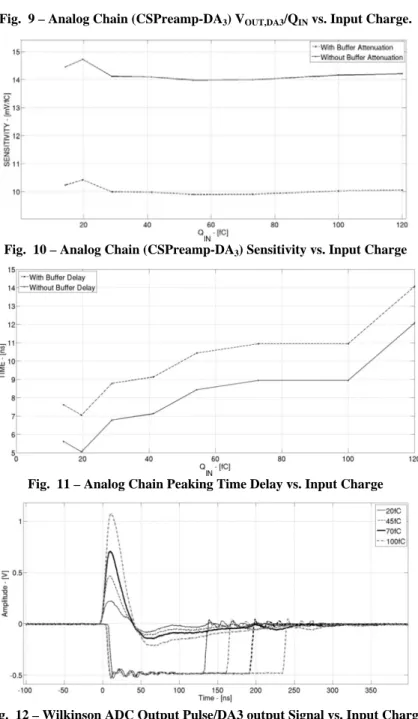
the output node common-mode voltage, for the following DA
1stage, which has NMOS input 114
transistors (for noise minimization).
115
Regarding CSPreamp noise and time-reponse, both are optimized by suitable input device 116
transconductance (g
m1). In this direction, transistor M
1operates in moderate inversion region 117
(V
ov≈100mV) with a nominal current of 1.6mA in order to have large g
m1=25mA/V, much larger 118
than in previous design. This improves both noise and speed, thanks to a better redistribution of 119
the power (which remains constant) among the different stages. Larger power is allocated to the 120
CSPreamp input stage, saving power elsewhere (mainly in the DAx chain, and in the bias 121
circuit), where it was not necessary. Such large g
m1value improves the speed-of-response as 122
follows. The CSPreamp transfer function is in first approximation given by:
123
124 (1)
125
Since g
m1=25mA/V and C
F≪ C
D, the zero is at much higher frequency and can be neglected.
126
Assuming infinite g
m1, the dominant pole is given by C
F·R
F, and the output pulse voltage peak 127
value should be approximately given by Q
IN/C
F≈7mV
0-PEAK. In this design g
m1has been fixed at 128
25mA/V, as trade-off between noise and power, resulting in a CSPreamp sensitivity of 129
1.4mV/fC. These considerations are validated by Fig. 4, where the simulated CSPreamp time 130
response is shown (NO-NOISE curve) and compared with the single-pole ideal system (No- 131
Noise, No-C
Dcurve). The main effects of the C
Dcapacitance are: lower sensitivity (4mV
0-PEAK132
vs. 6mV
0-PEAKfor minimum Q
IN=5fC) and slightly slower time response (7ns vs. 4ns).
133
134
Fig. 3 – 8xAFE Charge-Sensitive-Preamplifier Schematic.
135
136
– 5 –
Fig. 4 – CSPreamp. vout Transient Noise Time Response
137
138
Fig. 5 – CSPreamp-DA1-DA2-DA3 chain. AC Frequency Responses.
139
The large design g
m1not only avoids significant sensitivity degradation due to the large parasitic 140
C
D, but also mitigates the second pole effect, pushing it up to very much higher frequency, 141
hence improving the time performance of the CSPreamp (whose second pole time constant is 142
inversely proportional to g
m1, as stated in eq. 1).Such large g
m1enforces virtual ground and, then, 143
lowers CSPreamp equivalent input impedance down to ≈60Ω, (nominal, in order to be <120Ω 144
over PVT) acceptable for PTD, and noise. Two transient-noise iterations have been run, to 145
highlight the thermal noise contribution, resulting in 0.55mV
RMS-in-band output noise power.
146
The SNR at the CSPreamp output is 19dB in case of minimum input charge of 5fC, and it rises 147
up to 45dB at 100fC.
148
3.2 DA
1-DA
2-DA
3149
The CSPreamp output signal is amplified&filtered by the DA
1-DA
2-DA
3stages, which shape 150
the signal to convert the pulse into a bipolar shaping and to define the fall-down time. In this 151
DA
1-DA
2-DA
3chain, the scaled 0.35µm devices have been exploited in the reduction of the 152
parasitic capacitance, and, then in increasing the speed while reducing power consumption. The 153
frequency response at the output of each stage is plotted in
Fig. 5. The full chain exhibits a pass- 154
band characteristic with a 5MHz center frequency. The high-pass part, mainly imposed by DA
3, 155
shows a 30kHz corner frequency and a slope of +6dB/octave (1
st-order high-pass filter). The 156
band-pass section is the superposition of all 4 amplifier low-pass characteristics.
157 158
3.3 Wilkinson A/D 159
The DA
3output signal feeds to the Discriminator and the Wilkinson ADC (W-ADC) stage, to 160
provide information regarding the arrival time and the total amount of input charge at the 161
CSPreamp input node. The Discriminator is a comparator, which detects the presence of a 162
specific minimum charge at the CSPreamp input nodes and provides the charge arrival time, 163
and the Start-of-Conversion signal for the W-ADC. The W-ADC, instead, performs a Voltage- 164
to-Time conversion, as shown in
Fig. 6. The sample capacitor (C
H) is charged for a given time 165
range T
GW(programmable by the external between 8ns and 32ns). Such capacitance is then 166
discharged down to the zero-crossing instant. Charge and discharge phases depend on Φ
1and 167
Φ
2, such as on ON-OFF switches phases. Φ
1and Φ
2signals are complementary MOS switches.
168
The equivalent time-width needed to discharge the C
Hwill be proportional to the analog input 169
voltage and, as a consequence, to the equivalent amount of charge at the CSPreamp input nodes.
170
As in
Fig. 6with the same integration time T
GW, the higher is the analog voltage peak value (i.e.
171
– 6 –
the Q
INinput charge), the higher is the time needed to cross down the horizontal axis. The 172
transconductor stages design had to face the lower output impedance of the 0.35µm devices 173
w.r.t. the 0.5µm devices. Specific arrangements have then been adopted to guarantee the same 174
impedance level. On the other hand, the power here is unchanged since it fixed by C
Hvalue, 175
maintained =3pF to make negligible any parasitic effects.
176
177
Fig. 6 – Wilkinson-ADC Operating Principle.
178
4. Preliminary Measurements Result
179
The presented 8xAFEchip has been integrated in CMOS 0.13µm (Fig. 7 shows the chip photo).
180
The electrical characterization has been carried-out mounting the 8xAFEon the mezzanine 181
board, working in the same boundary conditions w.r.t. the ATLAS experiment environments.
182
The 8 channels are placed&routed in order to guarantee symmetrical paths w.r.t. the bias and 183
setting circuits (located in the center region of the layout top-view, and used to program/regulate 184
the discriminators thresholds, gain, etc). Each channel occupies 0.4mm
2. The total area 185
(including additional pads, JTAG, etc.) is about 6.38mm
2. All the presented measurements have 186
been performed using different equivalent input charge (Q
IN) in the 5fC÷100fC input range.
187
4.1 8xAFE Electrical Characterization 188
The analog section of the 8xAFE composed by the cascade of the CSPreamp and the DA
1-DA
2- 189
DA
3stages is here presented. Fig. 8 shows the output signal vs. time at DA
3output buffers test 190
pins (see
Fig. 2), hence some voltage peak drop (i.e. about 3dB and 2ns additional time delay) 191
and an additional PTD is expected w.r.t. the effective on-chip DA
3signal (really managed by 192
the ADC). The DA
3output voltage ranges from 90mV
0-PEAKup to 1.2V
0-PEAK.Fig. 9 and Fig. 10 193
shows the V
OUT,DA3/Q
INtrans-characteristic and the sensitivity that is 14-2mV/fC for minimum 194
Q
IN. Moreover, the sensitivity is quite constant over the input charge range, so no voltage swing 195
saturation is presented over the 5fC÷100fC range, resulting in a very linear behavior. Finally 196
Fig. 11 shows PTD: PTD is lower than 9ns for minimum Q
IN(5fC), and raises up to 12nsat 197
100fC. For sake of completeness, the Fig. 9-Fig. 12 are shown with and without the 198
amplitude/time effects of the test points output buffers. The Wilkinson ADC has bee also tested 199
for 4 different equivalent input charge values (in the 20fC÷100fC range). The output pulse 200
width is proportional to the equivalent amount of charge at the 8xAFE input, resulting in the 201
very linear characteristic in Fig. 13.
202
5. Conclusions
203
An 8-channels read-out front-end for MDT ATLAS detectors at CERN LHC has been 204
presented. The design has been carried-out in IBM 0.13µm technology, targeting area and noise 205
reduction at the same power budget of the state-of-the-art for ATLAS MDT detectors. Table I
206
– 7 –
summarizes the most important performance of the presented 8xAFE for the MDT-ATLAS- 207
read-out, compared with the previous implementation.
208
TABLE I.
S
TATE-
OF-
THE-A
RTC
OMPARISON209
Parameter This Work [3]
CMOS Technology 0.13µm@3.3V 0.5 µm@3.3V
Total Die Area 6.38mm
211.9mm
2Channel Current Consumption 10mA 11mA Detector Parasitic Cap. 60pF 60pF
Input Charge 5fC÷100fC 5fC÷100fC Front-End Delay at 100fC@Q
IN12ns ~ 15ns
Front-End Sensitivity 14mV/fC 8.9mV/fC
ENC 0.6fC 1fC
SNR 15dB 10.9dB
The device exhibits a factor 2 area reduction (lower than the CMOS scaling-down factor due to 210
0.35µm High-Voltage devices). For the same detector capacitance, the single channel power 211
consumption is approximately the same than in [3], whereas input charge signal quality 212
improves (higher SNR, given by better CSPreamp ENC noise performance). The peaking time 213
delay is 12ns, i.e. 3ns lower than the state-of-the-art, resulting in faster response and reduced 214
probability to muons data loss.
215
Fig. 7 – Chip Layout Photo. Fig. 8 – DA3 Test Point Buffers Output Signal vs. Input Charge (5fC÷100fC)
References 216
[1] The ATLAS collaboration, The ATLAS Experiment at the CERN Large Hadron Collider, Journal of Instrumentation 3 (2008)
217
[2] Y. Arai et al., ATLAS Muon Drift Tube Electronics, Journal of Instrumentation 3.09 (2008): P09001
218
[3] C. Posch, E. Hazen, J. Oliver, MDT-ASD, CMOS front-end for ATLAS MDT, ATL-MUON-2002-2003, September. 2007
219
[4] Y. Arai, C. Poschet al., On-Chamber Readout System for the ATLAS MDT Muon Spectrometer, IEEE Transactions on Nuclear
220
Science, vol. 51, no. 5, October 2004.
221
222
– 8 –
Fig. 9 – Analog Chain (CSPreamp-DA3) VOUT,DA3/QIN vs. Input Charge.
223
224
Fig. 10 – Analog Chain (CSPreamp-DA3) Sensitivity vs. Input Charge
![Fig. 1 – Muons Detection Scheme [2].](https://thumb-eu.123doks.com/thumbv2/1library_info/4010937.1541125/3.892.249.636.282.438/fig-muons-detection-scheme.webp)