The new octal amplifier-shaper-discriminator chip for the ATLAS MDT chambers at HL-LHC
S. Abovyan
a, V. Danielyan
a, M. Fras
a, O. Kortner
a, H. Kroha
a,∗, R. Richter
a, Y. Zhao
a, A. Baschirotto
b, M. De Matteis
b, F. Resta
ba
Max-Planck-Institute for Physics, Munich, Germany
b
University of Milan-Bicocca, Milan, Italy
Abstract
In order to fully exploit the physics potential of the ATLAS experiment at the HL-LHC, the trigger rate of and maximum latency of the first-level trigger system will be increased to 1 MHz and 10 s, respectively. In addition, a new first-level muon track trigger with high momentum resolution based on the ATLAS precision Muon Drift-Tube (MDT) chambers will be employed which requires triggerless readout. The TDC ASICs of the current front-end electronics of the MDT chambers are incompatible with these requirements. The front-end boards, each with a TDC chip and three 8-channel amplifier-shaper-discriminator (ASD) chips have to be replaced. Therefore, a new octal ASD2 ASIC has been developed in modern 130 nm IBM / Gobal Foundries CMOS technology.
The chip also contains a Wilkinson ADC to perform both time-over-threshold and signal charge measurement. The ASD design has been fully qualified for the serial production of 80000 chips for ATLAS. The performance in terms of signal rise time and channel uniformity significantly surpasses the one of the previous chip while keeping the power consumption constant. In addition to the characterisation with test pulses, several chips have been mounted on the front-end boards and tested in a muon beam at the Gamma Irradiation Facility GIF ++ at CERN up to high counting rates where the superior drift time and spatial resolution becomes evident.
Keywords: MDT chambers, ASD chip, High-Luminosity LHC, ATLAS experiment PACS: 29.40.Cs, 29.40.Gx
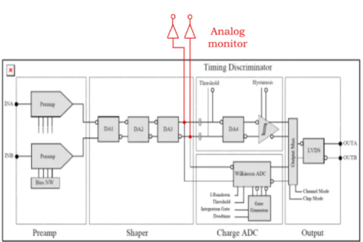
Analog monitor
Figure 1: Functionality diagram of the existing ASD and future ASD2 chips for the ATLAS MDT chambers at LHC and HL-LHC, respectively.
1. Functionality
The first processing stage of an ATLAS Monitored Drift Tube (MDT) readout electronics, the Amplifier-Shaper- Discriminator (ASD), largely determines the overall perfor- mance of the MDT chambers for crucial parameters like time resolution, channel uniformity, e ffi ciency and noise rejection.
∗
Corresponding author
Email address: kroha@mppmu.mpg.de (H. Kroha)
The MDT ASD is an 8-channel amplifier-shaper-discriminator ASIC with charge-to-time converter based on a Wilkinson ADC which has a variety of programmable parameters: the dis- criminator threshold and hysteresis, the channel dead-time, the charge integration time and the capacitor discharge current of the Wilkinson ADC. The ASD2 prototype design is done in the well-established and supported, radiation tolerant 130nm IBM CMOS 8RF-DM technology on the basis of the original ASD design features [1].
The ASD provides two modes of operation: Time-Over- Threshold (ToT) and ADC mode. Each ASD channel comprises an input stage, a charge sensitive preamplifier converting the in- put charge into a voltage, followed by three shaping stages, dis- criminator and the Wilkinson-type ADC, which is enabled de- pending on the operation mode. In ToT mode, the discriminator output is directly routed to the channel output pins. It reflects the crossing of the programmed threshold by the amplified and shaped signal. In the experiment, this threshold crossing deter- mines the arrival time of the ionization charges at the sense wire of the drift tubes. But because of finite rise time and bandwidth, the threshold crossing time depends on the signal charge and on the threshold itself. The ADC charge measurement is used to reduce this dependence in order to increase the accuracy of the time measurement (time slewing corrections).
The ADC measures the signal charge in a given time win- dow following the initial threshold crossing (charge integration gate) using the dual-slope Wilkinson technique where the am- plified input charge is collected on a capacitor during the pro-
Preprint submitted to Elsevier June 25, 2018
grammable integration window and then converted into a digital pulse width corresponding to the discharge time of the capacitor at a programmable discharge current (rundown current). Each ASD channel provides a di ff erential digital output, where the time of the leading edge corresponds to the ionization charge arrival time and the pulse width represents the charge in the leading edge of the input signal. This timing information is subsequently digitized by a TDC ASIC.
The ASD design uses a common DAC to provide the thresh- old for all 8 discriminators on the chip. Great emphasis was put on minimizing channel-to-channel gain variation and inter- nal o ff sets, to reduce intrinsic channel noise and crosstalk and to achieve high uniformity of the operating parameters among the channels of each chip (see [2] for more details on a pre- vious version of the chip). The analog path was modified and made fully di ff erential compared to the original ASD ASIC, where the preamplifier consisted of a single-ended (i.e. com- mon source) analog gain stage with feedback capacitor. Post- layout simulations validated this choice, demonstrating that un- wanted supply noise is attenuated of -7dB at the output of the first stage. The ASD2 ASIC occupies an area of 7.64 mm
2and has a sensitivity of about 10 mV / fC, 10 ns peaking time at the discriminator input and 10 mA current consumption per chan- nel at 3.3 V supply voltage.
2. Performance Tests
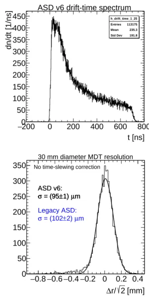
A full characterization of 18 chips has been performed. The test results (see for example Fig. 2) show excellent uniformity of the parameters of all channels on a chip (only 3-6 mV max- imum threshold spread) and also between di ff erent chips (only 8 mV threshold spread), a factor of 3 better than for the original chip made in 500 nm HP CMOS technology [1]. The labora- tory test results (on- and o ff -chamber) agree very well with the post-layout simulations for all performance parameters. Test- beam data taken with a small MDT chamber at CERN with and without γ background irradiation show that the new ASD ASIC performs equally well as the original chip on muon and γ sig- nals with respect to drift time and spatial resolution (see Figs. 2 and The peaking time is shorter than for the original chip by 2 ns resulting in better spatial resolution of the drift tubes (see Fig. 3) An irradiation test of the latest version of the chip at CERN showed no degradation of the functionality and perfor- mance for γ irradiation doses up to 1 MRad as expected for the 130 nm CMOS technology used.
After having successfully passed the required tests, the pro- duction of the 80,000 ASD2 chips required for the ATLAS MDT electronics upgrade for HL-LHC is foreseen in 2019- 2020.
References
[1] Y. Arai, et al., ATLAS Muon Drift Tube Electronics, J. Instr. 3.09 (2008) P09001.
[2] M. De Matteis, et al., Performance of the new Amplifier-Shaper- Discriminator chip for the ATLAS MDT chambers at the HL-LHC, J. In- str. 11.02 (2016) C02087.
Figure 2: Discriminator threshold scans of the 8 channels of a typical final ASD2 chip.
h_drift_time_1_25 Entries 113175 Mean 235.3 Std Dev 191.8
− 200 0 200 400 600 800 t [ns]
0 50 100 150 200 250 300 350 400 450
dn/dt [1/ns]
h_drift_time_1_25 Entries 113175 Mean 235.3 Std Dev 191.8