NEUTRON AND PROTON TESTS OF DIFFERENT TECHNOLOGIES FOR THE UPGRADE OF COLD READOUT ELECTRONICS OF THE ATLAS HADRONIC
ENDCAP CALORIMETER
M. NAGEL
Max-Planck-Institut f¨ur Physik, F¨ohringer Ring 6, 80805 Munich, Germany
E-mail: nagel@mppmu.mpg.de www.mppmu.mpg.de
on behalf of the HECPAS Collaboration
(IEP Koˇsice, Univ. of Montr´eal, MPI Munich, IEAP Prague, NPI ˇReˇz) The expected increase of total integrated luminosity by a factor of ten at the HL-LHC compared to the design goals for LHC essentially eliminates the safety factor for radiation hardness realized at the current cold amplifiers of the ATLAS Hadronic Endcap Calorimeter (HEC). New more radiation hard technologies have been studied: SiGe bipolar, Si CMOS FET and GaAs FET transistors have been irradiated with neutrons up to an integrated fluence of 2.2·1016n/cm2 and with 200 MeV protons up to an integrated fluence of 2.6·1014p/cm2. Comparisons of transistor parameters such as the gain for both types of irradiations are presented.
Keywords: ATLAS, Liquid Argon calorimeter, HL-LHC, cold readout electron- ics, radiation hardness
1. The ATLAS Hadronic Endcap Calorimeter
The hadronic endcap calorimeter (HEC) of the ATLAS experiment
1at the CERN Large Hadron Collider (LHC) is a copper-liquid argon sampling calorimeter in a flat plate design.
2,3The calorimeter provides coverage for hadronic showers in the pseudorapidity range 1.5 < |η| < 3.2. The HEC shares each of the two liquid argon endcap cryostats with the electromag- netic endcap (EMEC) and forward (FCAL) calorimeters, and consists of two wheels per endcap.
A HEC wheel is made of 32 modules, each with 40 liquid argon gaps, which are instrumented with active read-out pads. The signals from the
arXiv:1208.1989v1 [physics.ins-det] 9 Aug 2012
read-out pads are sent through short coaxial cables to preamplifier and summing boards (PSB) mounted on the perimeter of the wheels inside the liquid argon cryostat. The PSB boards carry highly-integrated preamplifier and summing amplifier chips in Gallium-Arsenide (GaAs) technology. The signals from a set of preamplifiers are summed to one output signal, which is transmitted to the cryostat feed-through.
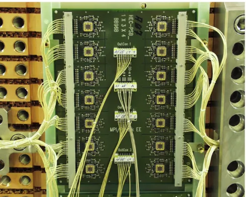
4Figure 1 shows a PSB board mounted and connected on the perimeter of a HEC wheel.
Fig. 1. A detailed view of a PSB board mounted on the perimeter of a HEC wheel.
2. Requirements of the HEC cold electronics for the HL-LHC upgrade
The GaAs technology currently employed in the HEC cold electronics has
been selected for its excellent high frequency performance, stable operation
at cryogenic temperatures, and radiation hardness. The radiation hardness
specifications were defined for ten years of operation at the LHC design
luminosity of 10
34cm
−2s
−1, including a safety factor of ten. For the high- luminosity upgrade of the LHC (HL-LHC), the luminosity is foreseen to increase by a factor of 5–10, effectively eliminating the safety factor. The ATLAS collaboration therefore decided to re-examine the radiation hard- ness of the current HEC cold electronics and of potential alternative tech- nologies.
5Detailed studies of the expected radiation levels after ten years of running under HL-LHC conditions yielded the following requirements (including a safety factor of 10) for the HEC cold electronics:
• Neutron fluence of 2 · 10
15n/cm
2• Proton fluence of 2 · 10
14p/cm
2• Gamma dose of 20 kGy
3. Tests
The neutron irradiation tests were performed at the ˇ Reˇ z Neutron Physics Laboratory near Prague in the Czech Republic, up to an integrated flu- ence of 2.2 · 10
16n/cm
2. A 37 MeV proton beam incident on a D
2O target created a somewhat divergent beam of neutrons with a flux density up to 10
11n/cm
2/s. The proton irradiation test were performed at the Pro- ton Irradiation Facility at the Paul-Scherrer-Institut in Switzerland with a 200 MeV proton beam up to an integrated fluence of 2.6 · 10
14p/cm
2. The transistors were bonded in ceramic casings and mounted on boards, which were then aligned in the particle beams. The three different tran- sistor technologies being tested were Si CMOS FET, SiGe Bipolar HBT (both SGB25V 250nm from IHP), and Triquint CFH800 250nm GaAs FET pHEMT, respectively. The performance of the transistors was monitored during irradiation with a vector network analyzer recording a full set of S-parameters. Beam current measurements and radiation films placed at various distances along the beam were used to determine the particle flux and the beam profile.
4. Results
The various transistor parameters were calculated from the measured S-
parameters using standard small signal circuit models. The transistor pa-
rameters were averaged over a certain frequency range to obtain their mean
and rms-values for every set of S-parameters. This frequency range ex-
tended from 300 kHz to 100 MHz, unless a certain parameter was unstable
at low or high frequencies, in which case appropriate cuts were applied.
These averaged transistor values were then used to characterize their be- haviour as a function of radiation.
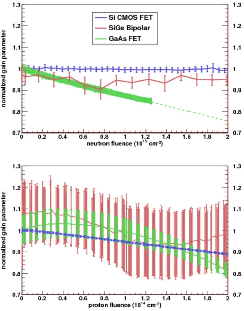
Fig. 2. Relative gain loss as a function of neutron (top) and proton (bottom) fluence for various technologies.
Figure 2 summarizes the results for the neutron (top) and the proton (bottom) tests in terms of the appropriate gain parameters. Displayed are the various gain parameters, i.e. the real part of the transconductance g
mfor the FET transistors and the current gain β for the Bipolar transistors, as a function of the corresponding particle fluence up to the required limit, normalized to the corresponding value before irradiation. We apply a linear fit to the observed radiation dependence, and the relative change of the gain parameter resulting from the fit is quoted in Table 1.
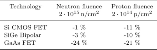
Table 1. Loss of gain of various technologies under neutron and proton irradiation.
Technology Neutron fluence Proton fluence 2·1015n/cm2 2·1014p/cm2
Si CMOS FET -1 % -11 %
SiGe Bipolar -3 % -10 %
GaAs FET -24 % -21 %