Neutron and proton tests of different technologies for the upgrade of the cold readout electronics of the ATLAS Hadronic End-cap Calorimeter
M Nagel
Max-Planck-Institut f¨ur Physik (Werner-Heisenberg-Institut), F¨ohringer Ring 6, 80805 Munich, Germany,www.mpp.mpg.de
E-mail: nagel@mpp.mpg.de
on behalf of the HECPAS Collaboration
(IEP Koˇ sice, Univ. of Montr´ eal, MPI Munich, IEAP Prague, NPI Reˇ ˇ z)
Abstract. The expected increase of total integrated luminosity by a factor ten at the HL- LHC compared to the design goals for LHC essentially eliminates the safety factor for radiation hardness realized at the current cold amplifiers of the ATLAS Hadronic End-cap Calorimeter (HEC). New more radiation hard technologies have been studied: SiGe bipolar, Si CMOS FET and GaAs FET transistors have been irradiated with neutrons up to an integrated fluence of 2.2·1016n/cm2 and with 200 MeV protons up to an integrated fluence of 2.6·1014p/cm2. Comparisons of transistor parameters such as the gain for both types of irradiations are presented.
1. The ATLAS Hadronic End-cap Calorimeter
The hadronic end-cap calorimeter (HEC) of the ATLAS experiment [1, 2] at the CERN Large Hadron Collider (LHC) is a copper-liquid argon sampling calorimeter in a flat plate design [3, 4]. The calorimeter provides coverage for hadronic showers in the pseudorapidity range 1.5 < |η| < 3.2. The HEC shares each of the two liquid argon end-cap cryostats with the electromagnetic end-cap (EMEC) and forward (FCAL) calorimeters, and consists of two wheels per end-cap, as illustrated in Figure 1.
A HEC wheel is made of 32 modules, each with 40 liquid argon gaps, which are instrumented
with active read-out pads. The signals from the read-out pads are sent through short coaxial
cables to preamplifier and summing boards (PSB) mounted on the perimeter of the wheels inside
the cryostat. The PSB boards carry highly-integrated preamplifier and summing amplifier chips
in Gallium-Arsenide (GaAs) technology. The signals from a set of preamplifiers are summed to
one output signal, which is transmitted to the cryostat feed-through [5]. Figure 2 shows a PSB
board mounted and connected on the perimeter of a HEC wheel.
Electromagnetic end-cap calorimeter Forward calorimeter
Feed-throughs and front-end crates Hadronic end-cap calorimeter
Figure 1. A liquid Argon end-cap cryostat, containing the hadronic and electromagnetic end- cap calorimeters, and the forward calorimeter [2].
Figure 2. A detailed view of a PSB board mounted on the perimeter of a HEC wheel [5].
2. Requirements of the HEC cold electronics for the HL-LHC upgrade
The GaAs technology currently employed in the HEC cold electronics has been selected for its excellent high frequency performance, stable operation at cryogenic temperatures, and radiation hardness. The radiation hardness specifications were defined for ten years of operation at the LHC design luminosity of 10
34cm
−2s
−1, including a safety factor of ten. For the high-luminosity upgrade of the LHC (HL-LHC), the luminosity is foreseen to increase by a factor of 5–10, effectively eliminating the safety factor. The ATLAS collaboration therefore decided to re- examine the radiation hardness of the current HEC cold electronics and of potential alternative technologies [6, 7]. Detailed studies of the expected radiation levels after ten years of running under HL-LHC conditions yielded the following requirements (including a safety factor of 10) for the HEC cold electronics [8]:
• 1 MeV equivalent neutron fluence (NIEL in Si) of 1.7 · 10
15n/cm
2• Total hadron fluence (SEE) of 1.8 · 10
14h/cm
2with E
h> 20 MeV
• Total ionization dose (TID) of 22 kGy
3. Tests
The neutron irradiation tests were performed at the Fast Neutron Facility at the Nuclear Physics Institute of the ASCR in ˇ Reˇ z near Prague, Czech Republic, up to an integrated fluence of 2.2 · 10
16n/cm
2(in terms of the 1 MeV equivalent NIEL in Si described in the next section). A 37 MeV proton beam incident on a D
2O target created a beam of neutrons with a continuous energy spectrum up to a maximum neutron energy of 34 MeV and a flux density up to 10
11n/cm
2/s with a 1/r
2decrease in flux density. The proton irradiation test were performed at the Proton Irradiation Facility at the Paul Scherrer Institute in Villigen, Switzerland, with a monoenergetic beam of 200 MeV protons up to an integrated fluence of 2.6 · 10
14p/cm
2. The transistors were bonded in ceramic casings and mounted on boards, which were then placed in a standard aluminum frame with 17 mm distance between slots and carefully aligned in the particle beams. The three different transistor technologies being tested were Si CMOS FET in SGB25V 250nm technology from IHP, SiGe Bipolar HBT (IHP SGB25V 250nm and IBM 8WLBiCMOS 130nm), and the GaAs FET currently used in ATLAS, either the Triquint CFH800 250nm transistors themselves or integrated into the HEC BB96 Preamplifiers and Systems. The performance of the transistors was monitored in situ during irradiation with a vector network analyzer recording a full set of S-parameters [9], which were converted to standard transistor parameters using suitable small signal circuit models.
4. Flux determination
A combination of radiation films and radmon diodes, placed at various slot positions along the beam, were used to determine the beam profile and, together with the beam current measurements, the particle flux. The films were exposed to a given beam current for various amounts of time and subsequently scanned. An iterative calibration procedure was used to obtain the dose as a function of net optical density [10], by combining the known relative dose measurements with the absolute normalization obtained from MC simulations and from the radmon diodes.
For the neutron test with its continuous neutron energy distribution, the fluence was scaled to
the 1-MeV equivalent neutron fluence in Silicon, employing the non-ionizing energy loss (NIEL)
scaling hypothesis [11], independent of the actual technology under irradiation. The divergent
nature of the neutron beam emerging from the heavy water target yielded a total fluence per
slot given by Φ = 3.22 · 10
16· (slot# +
173)
−2.11n/cm
2. At PSI in contrast, the almost collimated
proton beam together with an offset in the alignment of the boards yielded a basically constant
-2)
14 cm proton fluence (10
0 0.2 0.4 0.6 0.8 1 1.2 1.4 1.6 1.8
normalized gain parameter 0.8
0.9 1 1.1
SiGe Bipolar Si CMOS FET
GaAs FET
0.80.9 1 1.1
-2)
15 cm neutron fluence (10
0 0.2 0.4 0.6 0.8 1 1.2 1.4 1.6
normalized gain parameter 0.8
0.9 1 1.1
0.8 0.9 1 1.1
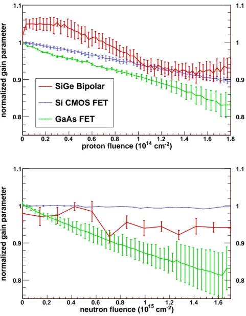
Figure 3. Relative gain loss as a function of proton (top) and neutron (bottom) fluence for the various technologies described in the legend. The respective gain parameters are described in the text. The data points represent the average of all the devices of a particular technology that were irradiated up to a given particle fluence; the error bars are the sample RMS [12].
fluence for all slots of Φ = (2.6 ± 0.4) · 10
14p/cm
2, where the main uncertainty stems from the unknown exact positions of the test structures inside the chip casing.
5. Results
The various transistor parameters were calculated from the measured S-parameters using
suitable small signal circuit models. The transistor parameters were averaged over a certain
frequency range to obtain their mean and rms-values for every set of S-parameters. This
frequency range extended from 300 kHz to 100 MHz, unless a certain parameter was unstable at
low or high frequencies, in which case appropriate cuts were applied. These averaged transistor
values were then used to characterize their behaviour as a function of particle fluence.
Table 1. Loss of gain of various transistor technologies under neutron and proton irradiation [12].
Technology Neutron fluence Proton fluence 1.7 · 10
15n/cm
21.8 · 10
14p/cm
2Si CMOS FET 0 % -11 %
SiGe Bipolar -5 % -7 %
GaAs FET -20 % -17 %
Figure 3 summarizes the results for the proton (top) and the neutron (bottom) tests in terms of the appropriate gain parameters as a function of the corresponding particle fluence up to the required limit, normalized to the corresponding value before irradiation. The various gain parameters are the real part of the transconductance g
mfor the FET transistors, the differential current gain β for the Bipolar transistors, and in case of the HEC BB96 preamplifiers and systems, where our simple transistor models are not applicable, the transresistance r
m=
∆Vout
∆Iin
= |S
21· Z
in|, which relates the output voltage to the input current, where Z
inis the input impedance. Displayed are the sample averages of all the devices of a particular technology under test at each of the two test facilities, that were irradiated up to a given particle fluence; the error bars represent the sample RMS. The relative change of the gain parameter is quoted in Table 1, where we also used a linear extrapolation of the gain parameter up to the required fluence for those devices that did not reach that fluence.
6. Summary
Our first observation is that proton irradiation seems to cause more damage to the electronics than neutron irradiation (at least for the Si CMOS and SiGe Bipolar transistors), despite the fact that an order of magnitude more neutrons than protons are expected to impact the HEC cold electronics. In the case of the GaAs FETs, the gain degradation is roughly the same for both types of irradiation, although a quantitative assessment suffers from the fact that two different gain parameters (transconductance vs. transresistance) are being compared.
It can be concluded that both the Si CMOS FETs and the SiGe Bipolar transistors considered as alternative technologies are more radiation hard than the currently used GaAs FETs. Among the alternative technologies, a preference would be given to the Si CMOS FETs, since the SiGe Bipolar transistors require a stabilization of their operation point, which would lead to a more complex circuitry to meet the same radiation hardness requirements.
The GaAs technology currently used in the HEC cold electronics degrades significantly at
the expected radiation levels, but it does not break down yet. The observed level of degradation
(∼20%) could conceiveably be compensated for by some sort of calibration procedure. But
before one can come to a decision whether it is safe or not to keep the current HEC cold
electronics for HL-LHC conditions, the impact of this level of degradation on the overall HEC
performance (e.g. in terms of jet energy resolution) needs to be better understood. In addition
to that, a measurement of the performance degradation in the cold is needed. A decision has
thus been reached to perform a more detailed study of the current HEC BB96 ASICs, including
characterization of the linearity of their response with realistic pulses as they appear in the
ATLAS detector, and a detailed simulation of the propagation of the ’degraded’ signals through
the summation, digitization, and reconstruction stages. This, and the measurement of the
performance degradation in the cold are both ongoing efforts.
References
[1] 1994 ATLAS: technical proposal for a general-purpose pp experiment at the Large Hadron Collider at CERN LHC Tech. Proposal (Geneva: CERN) cern-lhcc-94-43, lhcc-p-2
[2] Aad Get al.(ATLAS Collaboration) 2008J.Inst.3S08003 doi:10.1088/1748-0221/3/08/S08003
[3] ATLAS Collaboration (ATLAS) 1996 Atlas liquid argon calorimeter: Technical design report Tech. rep.
CERN cern-lhcc-96-41, atlas tdr 2
[4] Gingrich D M et al.(The ATLAS Hadronic End-Cap Calorimeter Group) 2007 J.Inst. 2 P05005 atl-larg- pub-2007-009, atl-com-larg-2007-006, mpp-2007-237
[5] Ban J, Brettel H, Cwienk W D, Fent J, Kurchaninov L, Ladygin E, Oberlack H, Schacht P, Stenzel H and Strizenec P 2006Nucl.Instrum.Meth.A556158–168 mpp-2005-193
[6] Vankov P 2012arXiv:1201.5469 ATL-UPGRADE-PROC-2012-003
[7] Schacht P 2010 Proceedings of the 11th ICATPP Conference on Astroparticle, Particle, Space Physics, Detectors and Medical Physics Applications (World Scientific) pp 392–403 ISBN 9789814307529 doi:10.1142/9789814307529 0065
[8] Baranov S, Bosman M, Dawson I, Hedberg V, Nisati A and Shupe M 2005 Estimation of radiation background, impact on detectors, activation and shielding optimization in atlas Tech. Rep. ATL-GEN-2005-001, ATL- COM-GEN-2005-001,CERN-ATL-GEN-2005-001 CERN Geneva (and unpublished updates)
[9] Dicke R H 1947J.Appl.Phys.18873 doi:10.1063/1.1697561
[10] Martiˇs´ıkov´a M and J¨akel O 2010Phys.Med.Biol.55N281–290 doi:10.1088/0031-9155/55/10/N03
[11] Vasilescu A 1997 The niel scaling hypothesis applied to neutron spectra of irradiation facilities and in the atlas and cms sct Tech. Rep. ROSE/TN/97-2 CERN
[12] Oberlack H, Dannheim D, Fischer A, Hambarzumjan A, Pospelov G, Reimann O, Rudert A and Schacht P 2009Nuclear Science Symposium Conference Record (NSS/MIC), 2009 IEEEpp 758–762 ISSN 1095-7863
![Figure 2. A detailed view of a PSB board mounted on the perimeter of a HEC wheel [5].](https://thumb-eu.123doks.com/thumbv2/1library_info/4026521.1542140/2.892.203.689.704.1096/figure-detailed-view-psb-board-mounted-perimeter-wheel.webp)
![Table 1. Loss of gain of various transistor technologies under neutron and proton irradiation [12].](https://thumb-eu.123doks.com/thumbv2/1library_info/4026521.1542140/5.892.256.636.229.343/table-loss-various-transistor-technologies-neutron-proton-irradiation.webp)
