PAPER • OPEN ACCESS
Electrically tunable exchange splitting in bilayer graphene on monolayer Cr 2 X 2 Te 6 with X = Ge, Si, and Sn
To cite this article: Klaus Zollner et al 2018 New J. Phys. 20 073007
View the article online for updates and enhancements.
Related content
Topological phases in two-dimensional materials: a review
Yafei Ren, Zhenhua Qiao and Qian Niu -
A first principles approach to magnetic and optical properties in single-layer graphene sandwiched between boron nitride monolayers
Ritwika Das, Suman Chowdhury and Debnarayan Jana
-
Graphene-based half-metal and spin- semiconductor for spintronic applications Jingshan Qi, Xiaofang Chen, Kaige Hu et al.
-
Recent citations
Magnetic proximity in a van der Waals heterostructure of magnetic insulator and graphene
Bogdan Karpiak et al -
New J. Phys.20(2018)073007 https://doi.org/10.1088/1367-2630/aace51
PAPER
Electrically tunable exchange splitting in bilayer graphene on monolayer Cr 2 X 2 Te 6 with X = Ge, Si, and Sn
Klaus Zollner
1,3, Martin Gmitra
1,2and Jaroslav Fabian
11 Institute for Theoretical Physics, University of Regensburg, D-93040 Regensburg, Germany
2 Institute of Physics, P. J.Šafárik University in Košice, 040 01 Košice, Slovakia
3 Author to whom any correspondence should be addressed.
E-mail:klaus.zollner@physik.uni-regensburg.de
Keywords:graphene, spintronics, heterostructures, proximity exchange
Abstract
We investigate the electronic band structure and the proximity exchange effect in bilayer graphene (BLG) on a family of ferromagnetic multilayers Cr
2X
2Te
6, X=Ge, Si, and Sn, with first principles methods. In each case the intrinsic electric field of the heterostructure induces an orbital gap on the order of 10 meV in the graphene bilayer. The proximity exchange is strongly band-dependent. For example, in the case of Cr
2Ge
2Te
6, the low energy valence band of BLG has exchange splitting of 8 meV, while the low energy conduction band’s splitting is 30 times less (0.3 meV). This striking discrepancy stems from the layer-dependent hybridization with the ferromagnetic substrate.
Remarkably, applying a vertical electric field of a few V nm
–1reverses the exchange, allowing us to effectively turn ON and OFF proximity magnetism in BLG. Such a field-effect should be generic for van der Waals bilayers on ferromagnetic insulators, opening new possibilities for spin-based devices.
1. Introduction
The properties of two-dimensional materials can be strongly altered by proximity effects in van der Waals heterostructures. One prominent example is graphene, which experiences strong proximity spin–orbit coupling ( SOC ) effects when placed on transition-metal dichalcogenides [ 1, 2 ] , and a giant fi eld-effect SOC when bilayer graphene (BLG) is used [3]. Typical experimental structures like graphene/hBN/ferromagnet, showing very ef fi cient spin injection [ 4 – 8 ] , also feature signi fi cant proximity exchange [ 9, 10 ] . These heterostructures are presently used in optospintronic devices [1, 11, 12] and also for spin transport [4–8] in graphene spintronics [ 13 ] . However, when it comes to device realizations, BLG offers many advantages, due to the possibility of having an electrically tunable band gap [14, 15], as well as the more precise control of the chemical potential [16, 17].
Graphene is a diamagnet. Can we make it ‘ferromagnetic’so that it could be used for spintronics applications [ 18, 19 ] ? It turns out that an effective way to achieve this is to place graphene on a ferromagnetic substrate (insulator or semiconductor, to preserve the Dirac character of the bands and avoid substrate transport).
Graphene then experiences proximity exchange coupling, typically in the range of 1 – 10 meV [ 9, 10, 20 – 29 ] , sometimes reaching even higher values [30–33]. Exchange proximity effects in graphene were observed by quantum anomalous Hall effect [20], magnetoresistance [22] and nonlocal spin transport experiments [21], as has been con fi rmed theoretically [ 26 – 30, 33 ] .
Several ferromagnetic insulators (FMI), like EuO and Yttrium–Iron–Garnet, have been considered in the context of graphene spintronics [ 22, 31 – 34 ] . However transition-metal trichalcogenides Cr
2Si
2Te
6, Cr
2Ge
2Te
6(CGT), and transition-metal trihalides CrI
3, and their monolayers are now extensively discussed in literature as promising materials for low-dimensional spintronics because of their FMI ground state properties [35–53].
These materials have attracted attention as substrates for topological insulators ( TI ) [ 49,50 ] and graphene [ 27 ] , because ferromagnetic coupling is present. For example, CGT seems to be a nice platform for large scale epitaxial growth of TIs with high quality interfaces, where the interaction of TI surface states and ferromagnetism can be
OPEN ACCESS
RECEIVED
16 April 2018
ACCEPTED FOR PUBLICATION
21 June 2018
PUBLISHED
4 July 2018
Original content from this work may be used under the terms of theCreative Commons Attribution 3.0 licence.
Any further distribution of this work must maintain attribution to the author(s)and the title of the work, journal citation and DOI.
© 2018 The Author(s). Published by IOP Publishing Ltd on behalf of Deutsche Physikalische Gesellschaft
studied [ 49, 50 ] . Moreover, fi rst principles calculations show that monolayer graphene on CGT [ 27 ] features exchange splitting of about 10 meV. It is then natural to try to use them for proximity effects in BLG.
For device operations, it is desirable to have electric control of the band structure and spin properties. We already know that BLG on a substrate can open a gap (similarly to having a vertical electric field applied). Could we also control exchange coupling in a similar way, simply applying an electric field? One naturally expects that the proximity effect is strongest in the BLG layer adjacent to the ferromagnetic substrate. Orbitals from this layer form, say, the valence band ( VB ) , which will exhibit strong exchange splitting. The conduction band ( CB ) , on the other hand, would have no or only weak splitting. If an electric fi eld is applied, the situation can be reversed, and now it would be the CB that has the largest exchange splitting. It has also been shown in model calculations, that BLG on a FMI can be a platform for field-effect magnetic or spin devices [54–58]. The combination of exchange and electric field leads to the control of the spin-dependent gap of the carriers and perfect switching of the spin- polarization is predicted [ 56, 57 ] . How realistic is such an electrical control of proximity exchange splitting in BLG on real magnetic substrates? We answer this question by performing density functional theory ( DFT ) calculations of BLG on monolayer Cr
2Si
2Te
6, CGT, and Cr
2Sn
2Te
6. Indeed, we show that the exchange splitting in a given band can be switched ON and OFF by a relatively modest vertical electric field. This opens venues for investigating magnetotransport in BLG, as well as for controlling the ‘synthetic’ magnetism by gates. The analogy with spin–
orbit valve effect [3] is certainly there. But the exchange valve is fundamentally different, in that it generates a magnetic moment in BLG, splits the two valleys equally, and opens up a new platform for magnetotransport phenomena a spin fi ltering. There are now recent experiments demonstrating an electric fi eld control of ferromagnetism in 2D ferromagnets ( such as CrI
3[ 59 ] and CGT [ 60 ]) . Controlling ‘ synthetic ’ magnetism in BLG on such materials would be a great achievement.
In this paper we investigate, by performing first principles calculations, the proximity induced exchange coupling in BLG on monolayer CGT, as well as on Cr
2Si
2Te
6and Cr
2Sn
2Te
6( the last has been theoretically predicted [ 61 ] but not yet prepared experimentally ) . We fi nd that the low energy bands of BLG show an indirect band gap of roughly 17 meV, which can be ef fi ciently tuned by experimentally accessible electric fi elds of a few V nm
–1. The proximity induced exchange splitting of the VB is giant, being around 8meV, 30 times larger than the exchange splitting in the CB. This large difference arises from the fact, that the VB is formed by non-dimer carbon atoms from the bottom graphene layer directly above CGT, where the proximity effect is strong, while the CB is formed by non-dimer carbon atoms from the top graphene layer, where the proximity effect is weak ( in BLG with Bernal stacking, one pair of carbon atoms is vertically connected, which we call dimer, the other pair non-dimer ) . The most interesting result is the switching of the exchange splitting from the valence to the CB, via an external electric field that counters the built-in field of the BLG/CGT heterostructure. A proximity exchange valve is realized. We also include a brief discussion on possible device geometries based on the field-effect proximity exchange.
2. Computational details and geometry
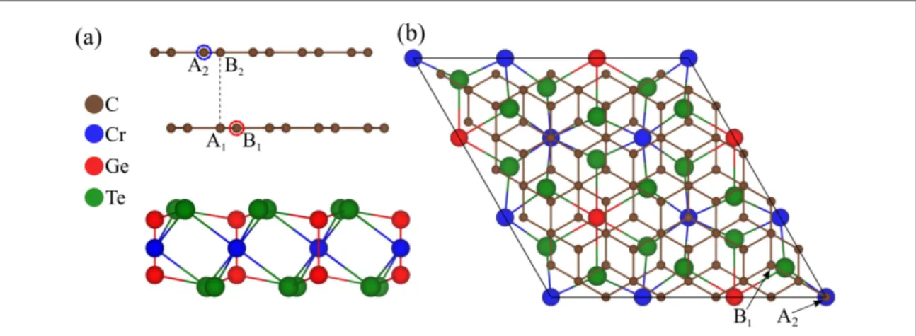
The heterostructure of BLG on CGT is shown in figure 1, where a 5×5 supercell of BLG is placed on a 3 ´ 3 CGT supercell. The considered heterostructure model contains 130 atoms in the unit cell. We keep the lattice constant of graphene unchanged at a=2.46 Åand stretch the lattice constant of CGT by roughly 4%
from 6.8275Å [36] to 7.1014Å. Theoretical calculations predict that the tensile strain leaves the ferromagnetic ground state unchanged, but enhances the band gap and the Curie temperature of CGT [46, 43]. In figure 1(a) the side view of the structure shows the Bernal stacking of BLG, with an average distance relaxed to
3.266 Å between the graphene layers, in good agreement with experiment [ 62 ] . The average distance between the lower graphene layer and CGT was relaxed to 3.516Å, consistent with literature [27].
Previous calculations show that the relative alignment of graphene on CGT does not influence the electronic bands much, see [27], and we will only consider the supercell with stacking as in figure 1. We will also not consider SOC in the calculation, since it was shown that proximity induced exchange in graphene, caused by CGT, is one order of magnitude larger than proximity SOC [ 27 ] . The electronic structure calculations and structural relaxation of BLG on CGT were performed by means of DFT [63] within Quantum ESPRESSO [64].
Self-consistent calculations were performed with the k point sampling of 18×18×1 to get converged results for the proximity exchange splittings. We have performed open shell calculations that provide the spin polarized ground state with a collinear magnetization. Theory and experiment predict that CGT is a FMI with magnetic anisotropy favoring a magnetization perpendicular to the CGT-plane [ 35 – 40, 50, 61 ] . A Hubbard parameter of U = 1 eV was used for Cr d-orbitals, being in the range of proposed U values especially for this compound [ 39 ] . The value results from comparison of DFT and experiment on the magnetic ground state of bulk CGT. Other theoretical calculations report, that their results are qualitatively independent from the used U values [46, 45].
We used an energy cutoff for charge density of 500Ry, and the kinetic energy cutoff for wavefunctions was 60Ry
for the scalar relativistic pseudopotential with the projector augmented wave method [65] with the Perdew–
Burke – Ernzerhof exchange correlation functional [ 66 ] . For the relaxation of the heterostructures, we added van der Waals corrections [ 67, 68 ] and used quasi-Newton algorithm based on trust radius procedure. In order to simulate quasi-2D systems the vacuum of 20 Åwas used to avoid interactions between periodic images in our slab geometry. Dipole corrections [69] were also included to get correct band offsets and internal electric fields.
To determine the interlayer distances, the atoms of BLG were allowed to relax only in their z positions ( vertical to the layers ) , and the atoms of CGT were allowed to move in all directions, until all components of all forces were reduced below 10
−3[Ry/a
0], where a
0is the Bohr radius.
3. Electronic band structure of BLG on CGT
The electronic structure of bare BLG contains four parabolic bands near the Fermi energy [70, 71]. Two low energy bands close to the charge neutrality point are formed by (p
z) orbitals of non-dimer atoms B
1and A
2, see figure 1. In addition, there are two higher lying bands formed by the orbitals of dimer atoms A
1and B
2, see fi gure 1. Since the dimer atoms are connected by direct interlayer hopping, the bands are shifted roughly 400 meV from the Fermi level, such that they can be ignored for transport.
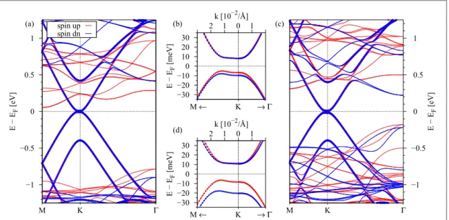
In fi gure 2 ( a ) we show the calculated electronic band structure of BLG on monolayer CGT along high symmetry lines. The bands near the Fermi level resemble closely the bands from bare BLG [ 70, 71 ] , even though the high energy CB of BLG is located within the CBs of CGT. Very important for transport is that the low energy bands of BLG are located within the band gap of CGT. The offset between the CB of BLG at K and the bottom of CB minimum of CGT is roughly 100 meV.
However, there are two important differences compared to bare BLG. First, the heterostructure possesses an intrinsic dipole (vertical to the sheets) and thus the two graphene layers are at a different potential energy resulting in a small indirect orbital gap of roughly 17 meV, see fi gure 2 ( b ) . The dipole of 1.505 Debye points from CGT towards BLG and therefore B
1(A
2) electrons have lower(higher) energy forming the valence (conduction) states. Second, the ferromagnetic CGT substrate interacts mainly with the lower graphene layer and, by proximity exchange, splits the low energy bands originating from this graphene layer by 8meV, see fi gure 2 ( b ) . The upper graphene layer is far away and experiences almost no proximity effect, resulting in a comparatively small spin splitting of the corresponding bands. The calculated magnetic moment of the Cr- atoms is positive and roughly 3.2 μ
B, but the Te-atoms and consequently the C-atoms are polarized with a small negative magnetic moment. Thus the BLG low energy VB is spin split, with spin down states being lower in energy, see fi gure 2 ( b ) . We would also like to emphasize, that due to the ferromagnetic substrate we break time- reversal symmetry. Thus the band structure and also the splitting is the same for K and K ’ point, see fi gures 2 ( b ) , (c). This is in contrast to proximity SOC in BLG on WSe
2[3], where K and K’ point are connected by time- reversal symmetry.
Figure 1.(a)Side view of bilayer graphene on monolayer Cr2Ge2Te6(supercell)with labels for the different atoms. LabelsA1,B1,A2 andB2indicate the sublattices of bilayer graphene in Bernal stacking. Orbitals on non-dimer atomsB1andA2form the low energy valence and conduction bands in the electronic structure of bilayer graphene, withB1being closer to the substrate.(b)Top view of the atomic structure of bilayer graphene on monolayer Cr2Ge2Te6, showing the positions ofB1andA2above CGT.
3
New J. Phys.20(2018)073007 K Zollneret al
4. Proximity exchange valve
In order to design devices for spintronics it is desirable if one can electrically control both spin and orbital properties. Such a control should be highly efficient in our heterostructures. In figure 3 we show the low energy band structures of BLG, in the presence of a vertical electric fi eld. At zero fi eld strength, see fi gure 3 ( c ) , the situation is as explained above; the hole band formed by p
z-orbitals of B
1is strongly split by proximity exchange, while the electron band, formed by p
z-orbitals of A
2is much less split. The reason is simply because the atoms B
1are closer to the ferromagnetic substrate experiencing a stronger proximity effect than atoms A
2. The ordering of the bands is determined by the built-in electric fi eld, pointing from CGT towards BLG, and thus B
1electrons are at lower energy.
Now, if we apply a positive external electric field, it adds to the internal field, opening the orbital gap further, keeping the band-dependent exchange splitting unchanged. But when the applied fi eld is negative and strong enough to compensate the built-in electric field, the orbital gap closes, see figure 3(b). This compensation happens at roughly −0.375V nm
–1and the states from atomsB
1and A
2are almost at the same potential energy, closing the gap.
A further increase of the negative field leads to the reopening of the band gap, see figure 3(a), but with a switched character of the bands. Now, the CB is formed by atoms B
1, which still experience the stronger proximity effect, while the VB is formed by atoms A
2, which are far from the ferromagnetic substrate. The switching of the band character happens, because the total (external and built-in) field is pointing now from BLG towards CGT, opposite to the zero field case. Thus, atoms B
1experience a higher potential than atoms A
2. We get a proximity exchange valve.
Are the relevant BLG low energy bands still within the orbital band gap of CGT? In figure 4(a), we see that the calculated dipole depends linearly on the applied electric field. The built-in dipole is roughly compensated by an external fi eld of − 0.4 V nm
–1; the amplitude of the intrinsic fi eld is 0.406 V nm
–1. Figure 4 ( a ) also shows that the energy offset between the BLG CB at K and the bottom of the CB minimum of CGT also changes with electric field. However, it is important to note that the low energy states of BLG are located within the band gap of CGT for electric fi elds that allow to observe the proximity exchange switching of the states. For fi elds larger than 0.5V nm
–1, the CB of BLG at K is shifted above the bottom of the CB minimum of CGT and BLG gets hole doped.
Figure 2.(a)Calculated electronic band structure of bilayer graphene on monolayer Cr2Ge2Te6. Bands of bilayer graphene are highlighted by blue and red circles.(b)Zoom to thefine structure of the low energy bands atKpoint close to the Fermi level.(c)Same as(b), but forK’point. Bands with spin up(down)are shown in red(blue).
In figure 4(b), we show the evolution of the exchange splittings and the orbital gap as a function of the applied electric fi eld. For this we de fi ne the orbital gap Δ , as the average of the spin up ( D
) and spin down ( D
) orbital gaps, D = D + D (
) 2 at the K point. The exchange splitting is de fi ned as the energy difference between spin up and spin down band, l
ex= E
- E
, at the K point for CB and VB, respectively. The orbital gap, which is a measure for the strength of the intrinsic dipole across the junction, is consistent with our dipole values. In figure 4(b), we see that the gap Δ has its minimum value, when the applied field compensates the intrinsic dipole, at around −0.4V nm
–1. If we look at the two splitting parameters l
exVBand l
exCB, we can see that there is a very nice switching behavior around −0.4V nm
–1, where the gap Δ has its minimum. The CB splitting l
exCBis around 7.5meV for fields smaller than −0.4V nm
–1and then drops to a small negative value when applying a larger field strength. The opposite behavior is observed for the VB splitting l
exVB, which has a large
Figure 3.Calculated sublattice resolved band structures aroundKvalley for vertical electricfield of(a)−0.75V nm–1,(b)
−0.375V nm–1,(c)0.0V nm–1. The circles radii correspond to the probability of the state being localized on carbon atomsB1(red filled circles)and atomsA2(blue open circles).
Figure 4.Calculated electricfield dependencies in bilayer graphene on monolayer Cr2Ge2Te6of(a)dipole induced in the
heterostructure(red), and energy offset(blue)of the bilayer graphene conduction band atKpoint and bottom of the conduction band minimum of the Cr2Ge2Te6.(b)Calculated band gapΔ, valence band splittinglexVBand conduction band splittinglexCBat theKpoint as a function of the applied electricfield.
5
New J. Phys.20(2018)073007 K Zollneret al
magnitude for fi elds larger than − 0.4 V nm
–1, see fi gure 4 ( b ) . We fi nd that the switching happens within a few hundred millivolts per nanometer, and most important at experimentally accessible fi eld strengths.
5. BLG on Cr
2Si
2Te
6and Cr
2Sn
2Te
6We predict similar scenarios for X=Si and Sn. In figure 5 we show the band structure of BLG on Cr
2Si
2Te
6and Cr
2Sn
2Te
6. Very similar to the bands of BLG on CGT, we see proximity spin splitting in the low energy VB, much larger than in the CB. Here we would like to mention that the compounds with Si and Ge have been identi fi ed in experiments [ 35, 36 ] , whereas the compound with Sn atoms has been only predicted theoretically [ 61 ] so far.
In the Si (Sn) case, proximity induced exchange is smaller (larger), as the VB spin splitting is about 3meV (12 meV) at the K point and the indirect gap is roughly 13meV (17 meV). The energy offset between the CB of BLG at K and the bottom of CB minimum of Cr
2Si
2Te
6(Cr
2Sn
2Te
6) is roughly 44meV (211 meV). The intrinsic dipole is weaker (stronger), about 1.336(2.013)Debye, which in the end leads to slightly different electric fields to observe the switching of the band character, as shown for BLG on CGT. The average distance between the lower graphene layer and Cr
2Si
2Te
6(Cr
2Sn
2Te
6) was relaxed to 3.563(3.531)Å. From the minimal difference in distance, we conclude that the spin splitting strongly depends on the material itself, whereas in [27], it was already shown that proximity induced exchange splitting strongly depends on the distance between graphene and the CGT substrate.
For model transport calculations it is useful to have realistic parameters in order to estimate the conductance through BLG in this heterostructures. In table 1 we summarize the most relevant parameters for BLG on all three considered substrates, for zero applied external field. The exchange splitting of the VB is always roughly 30 times larger than the splitting of the CB, independent of the material. Note that l
exCBhas the opposite sign of l
exVB, see table 1, meaning that the order of the spin bands for CB is different from the VB, at the K point.
6. BLG device
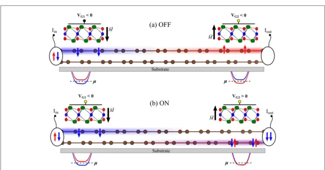
The electrical switching of the exchange splitting is a nice platform to realize novel spintronics devices, particularly since high spin-polarization can be achieved. Indeed, without any applied field, the chemical potential can be tuned close to the maximum of the VB where states are 100% spin polarized. The same would hold for the CB in an applied negative field. Based on theoretical model calculations—on magnetoresistance in BLG [72] and spin transport in graphene [29, 73], both being subject to proximity exchange—model transport calculations in FMI/BLG were performed [54, 55]. It was found that the proximity induced spin splitting allows BLG to act as a spin fi lter and spin rotator, being electrically controllable.
In figure 6 we show the structure of a spin filter, where BLG is deposited on an insulating substrate. On top of BLG we have two regions where CGT is placed, but in principle also other FMIs (YIG, EuO, CrI
3) are possible
Figure 5.(a)Calculated electronic band structure of bilayer graphene on monolayer Cr2Si2Te6. Bands of bilayer graphene are highlighted by blue and red circles.(b)Zoom to thefine structure of the low energy bands close to the Fermi level. Bands with spin up (down)are shown in red(blue),(c)and(d)are the same as(a)and(b), but for bilayer graphene on Cr2Sn2Te6.
candidates to realize the following devices. On top of the regions with the FMIs, gate voltages V
G1and V
G2can be applied. The magnetization directions M of the two FMIs are opposite.
Suppose the gate voltage V
G1is negative, then the low energy CBs of BLG below that first FMI are formed by the upper graphene layer and are strongly spin split, see figure 6(a). A spin unpolarized current is injected from the left and enters the fi rst heterostructure. If the chemical potential μ is between the two spin split electron bands, one spin component is filtered. In the central part we have just bare BLG where, due to small intrinsic SOC, the spin keeps its direction aligned until it enters the second heterostructure. Depending on the gate voltage V
G2, we can have a ON or an OFF state. Since the magnetization of the second FMI is opposite to the fi rst one the electrons cannot travel on in the upper layer if V
G2is also negative, because only the opposite spin channel is open, see figure 6(a). However, if V
G2is positive, the CBs are formed by the lower graphene layer, having almost no proximity exchange, and the electrons have both spin channels open, see fi gure 6 ( b ) .
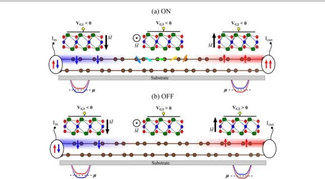
A different approach is based on the spin rotation, see fi gure 7. Similar to the spin fi lter, we polarize fi rst a spin unpolarized current injected from the left, which is then analyzed in the right heterostructure. The
Table 1.Summary of parameters for bilayer graphene on monolayer Cr2X2Te6for zerofield and X=Si, Ge, and Sn. The parameterΔdescribes the average orbital gap in the spectrum atK,λexare the exchange splittings for valence band(VB)and conduction band(CB)atK. The strength of the calculated intrinsic dipole across the heterostructure is given in debye, andd is the average distance between the lower graphene layer and the substrate.
The lattice constanta0is the one from the ferromagnetic substrate. In order to match the 5×5 graphene unit cell on the FMI we had to stretch its lattice constant to 7.1014Å. The strain gives, by how much we stretch the substrate. FinallyTcis the Curie temperature, either from experiment(exp.) on bulk samples or from Monte-Carlo simulations(theo.)on monolayers.
Cr2Si2Te6 Cr2Ge2Te6 Cr2Sn2Te6
Δ[meV] 16.15 22.55 25.15
lexVB[meV] 3.0 8.2 11.8
lexCB[meV] −0.1 -0.3 -0.5
dipole[debye] 1.336 1.505 2.013
d[Å] 3.563 3.516 3.531
a0[Å] 6.758[35] 6.828[36] 7.010[61]
strain[%] 5.1 4.1 1.3
Tc[K] 33(exp.[35]), 61(exp.[36]), 170 (theo.[61]) 90(theo.[61]) 130
(theo.[61])
Figure 6.Schematics of a spinfilter device, consisting of BLG on a substrate with two regions of a FMI(such as CGT)on BLG, where the two FMIs have opposite magnetization aligned along−zandz. Below each heterostructure region the low energy conduction bands are depicted. Spins are shown as red(spin up)and blue(spin down)arrows. Depending on the gate voltageVG2we can switch into(a)OFF state and(b)ON state.
7
New J. Phys.20(2018)073007 K Zollneret al
difference is that there is an additional FMI able to control the carrier spins via gate voltage V
G3. The
magnetization directions of the FMIs from left to right are − z, y, z and spin rotation happens below the central FMI. Depending on the gate voltage V
G3, carriers will flip their spin in the central region and the channel on the right is open, see fi gure 7 ( a ) , or closed, see fi gure 7 ( b ) . The origin of spin rotation and the ef fi ciency of this device has been discussed in [ 54, 55 ] , and is based on wave function localization and short ranged proximity exchange.
Above are but a few examples of spin devices based on the field-effect exchange coupling concepts. BLG on ferromagnetic insulating substrates could be employed to build bipolar spintronics elements, such as spin diodes and spin transistors [ 74 ] or spin logic devices [ 75 ] , which require exchange coupling ( but non necessarily magnetic moments) to make their electronic bands spin-dependent.
7. Summary and conclusion
In conclusion, we have studied from first principles the electronic structure of BLG on Cr
2Ge
2Te
6. We have shown that we can ef fi ciently, and most important fully electrically, switch the exchange interaction by one order of magnitude, of electrons and holes. At low enough energy the electronic states can be 100% spin polarized, which can lead to interesting new device concepts. We also expect that our DFT-derived parameters will be useful in model transport calculations involving exchange proximitized BLG.
Acknowledgments
This work was supported by DFG SPP 1666, SFB 689, SFB 1277 ( A09 and B07 ) , and by the European Unions Horizon 2020 research and innovation programme under Grant agreement No. 696656. The authors gratefully acknowledge the Gauss Center for Supercomputing e.V. for providing computational resources on the GCS Supercomputer SuperMUC at Leibniz Supercomputing Center.
ORCID iDs
Klaus Zollner https: // orcid.org / 0000-0002-6239-3271 Martin Gmitra https://orcid.org/0000-0003-1118-3028 Jaroslav Fabian https://orcid.org/0000-0002-3009-4525
Figure 7.Schematics of the spin rotator device. The magnetization directions of the FMIs from left to right are−z,y,zand spin rotation happens below the central FMI. Depending on the gate voltageVG3we can switch(a)ON or(b)OFF the spin rotation of the conduction electrons.
References
[1]Gmitra M and Fabian J 2015Phys. Rev.B92155403
[2]Gmitra M, Kochan D, Högl P and Fabian J 2016Phys. Rev.B93155104 [3]Gmitra M and Fabian J 2017Phys. Rev. Lett.119146401
[4]Gurram M, Omar S and van Wees B J 2017Nat. Commun.8248
[5]Kamalakar M V, Dankert A, Bergsten J, Ive T and Dash S P 2014Sci. Rep.46146
[6]Yamaguchi T, Inoue Y, Masubuchi S, Morikawa S, Onuki M, Watanabe K, Taniguchi T, Moriya R and Machida T 2013Appl. Phys.
Express6073001
[7]Kamalakar M V, Dankert A, Kelly P J and Dash S P 2016Sci. Rep.621168
[8]Fu W, Makk P, Maurand R, Bräuninger M and Schönenberger C 2014J. Appl. Phys.116074306 [9]Zollner K, Gmitra M, Frank T and Fabian J 2016Phys. Rev.B94155441
[10]LazićP, Belashchenko K D andŽutićI 2016Phys. Rev.B93241401
[11]Avsar A, Unuchek D, Liu J, Sanchez O L, Watanabe K, Taniguchi T, Özyilmaz B and Kis A 2017ACS Nano1111678–86 [12]Luo Y K, Xu J, Zhu T, Wu G, McCormick E J, Zhan W, Neupane M R and Kawakami R K 2017Nano Lett.173877–83 [13]Han W, Kawakami R K, Gmitra M and Fabian J 2014Nat. Nanotechnol.9794–807
[14]Zhang Y, Tang T T, Girit C, Hao Z, Martin M C, Zettl A, Crommie M F, Shen Y R and Wang F 2009Nature459820–3 [15]Oostinga J B, Heersche H B, Liu X, Morpurgo A F and Vandersypen L M K 2008Nat. Mater.7151–7
[16]Martin J, Akerman N, Ulbricht G, Lohmann T, Smet J H, von Klitzing K and Yacoby A 2008Nat. Phys.4144–8 [17]Rutter G M, Jung S, Klimov N N, Newell D B, Zhitenev N B and Stroscio J A 2011Nat. Phys.7649–55 [18]ŽutićI, Fabian J and Das Sarma S 2004Rev. Mod. Phys.76323–410
[19]Fabian J, Matos-Abiague A, Ertler C, Stano P andŽutićI 2007Acta Phys. Slovaca57342 [20]Wang Z, Tang C, Sachs R, Barlas Y and Shi J 2015Phys. Rev. Lett.114016603
[21]Leutenantsmeyer J C, Kaverzin A A, Wojtaszek M and van Wees B J 20162D Mater.4014001
[22]Mendes J B S, Alves Santos O, Meireles L M, Lacerda R G, Vilela-Leão L H, Machado F L A, Rodríguez-Suárez R L, Azevedo A and Rezende S M 2015Phys. Rev. Lett.115226601
[23]Sakai Set al2016ACS Nano107532–41
[24]Swartz A G, Odenthal P M, Hao Y, Ruoff R S and Kawakami R K 2012ACS Nano610063–9 [25]Wei Pet al2016Nat. Mater.15711–6
[26]DyrdałA and BarnaśJ 20172D Materials4034003
[27]Zhang J, Zhao B, Yao Y and Yang Z 2015Phys. Rev.B92165418 [28]Song Y 2018J. Phys. D: Appl. Phys.51025002
[29]Haugen H, Huertas-Hernando D and Brataas A 2008Phys. Rev.B77115406 [30]Zhang J, Zhao B, Yao Y and Yang Z 2015Sci. Rep.510629
[31]Yang H X, Hallal A, Terrade D, Waintal X, Roche S and Chshiev M 2013Phys. Rev. Lett.110046603 [32]Hallal A, Ibrahim F, Yang H, Roche S and Chshiev M 20172D Mater.4025074
[33]Su S, Barlas Y, Li J, Shi J and Lake R K 2017Phys. Rev.B95075418
[34]Singh S, Katoch J, Zhu T, Meng K Y, Liu T, Brangham J T, Yang F, Flatté M E and Kawakami R K 2017Phys. Rev. Lett.118187201 [35]Carteaux V, Ouvrard G, Grenier J C and Laligant Y 1991J. Magn. Magn. Mater.94127–33
[36]Carteaux V, Brunet D, Ouvrard G and Andre G 1995J. Phys.: Condens. Matter769–87
[37]Williams T J, Aczel A A, Lumsden M D, Nagler S E, Stone M B, Yan J Q and Mandrus D 2015Phys. Rev.B92144404 [38]Casto L Det al2015APL Mater.3041515
[39]Gong Cet al2017Nature546265–9
[40]Zhang X, Zhao Y, Song Q, Jia S, Shi J and Han W 2016Jpn. J. Appl. Phys.55033001 [41]Siberchicot B, Jobic S, Carteaux V, Gressier P and Ouvrard G 1996J. Phys. Chem.1005863–7 [42]Lin M Wet al2016J. Mater. Chem.C4315–22
[43]Chen X, Qi J and Shi D 2015Phys. Lett.A37960–3 [44]Liu Y and Petrovic C 2017Phys. Rev.B96054406
[45]Sivadas N, Daniels M W, Swendsen R H, Okamoto S and Xiao D 2015Phys. Rev.B91235425 [46]Li X and Yang J 2014J. Mater. Chem.C27071
[47]Lin G Tet al2017Phys. Rev.B95245212 [48]Xing Wet al20172D Mater.4024009
[49]Alegria L D, Ji H, Yao N, Clarke J J, Cava R J and Petta J R 2014Appl. Phys. Lett.105053512 [50]Ji Het al2013J. Appl. Phys.114114907
[51]Huang Bet al2017Nature546270–3
[52]Liu J, Sun Q, Kawazoe Y and Jena P 2016Phys. Chem. Chem. Phys.188777–84 [53]McGuire M 2017Crystals7121
[54]Michetti P, Recher P and Iannaccone G 2010Nano Lett.104463–9 [55]Michetti P and Recher P 2011Phys. Rev.B84125438
[56]Jatiyanon K, Tang I M and Soodchomshom B 2016Chin. Phys.B25078104 [57]Yu Y, Liang Q and Dong J 2011Phys. Lett.A3752858–62
[58]Rashidian Z, Mojarabian F M, Bayati P, Rashedi G, Ueda a and Yokoyama T 2014J. Phys.: Condens. Matter26255302 [59]Jiang S, Li L, Wang Z, Mak K F and Shan J 2018Nat. Nanotechnol.(https://doi.org/10.1038/s41565-018-0135-x) [60]Wang Zet al2018 arXiv:1802.06255
[61]Zhuang H L, Xie Y, Kent P R C and Ganesh P 2015Phys. Rev.B92035407 [62]Baskin Y and Meyer L 1955Phys. Rev.100544–544
[63]Hohenberg P and Kohn W 1964Phys. Rev.136B864–71 [64]Giannozzi Pet al2009J. Phys.: Condens. Matter21395502 [65]Kresse G and Joubert D 1999Phys. Rev.B591758–75
[66]Perdew J P, Burke K and Ernzerhof M 1996Phys. Rev. Lett.773865–8 [67]Grimme S 2006J. Comput. Chem.271787–99
[68]Barone V, Casarin M, Forrer D, Pavone M, Sambi M and Vittadini A 2009J. Comput. Chem.30934–9 [69]Bengtsson L 1999Phys. Rev.B5912301–4
9
New J. Phys.20(2018)073007 K Zollneret al
[70]Nilsson J, Castro Neto A H, Guinea F and Peres N M R 2008Phys. Rev.B78045405 [71]McCann E and Koshino M 2013Rep. Prog. Phys.76056503
[72]Semenov Y G, Zavada J M and Kim K W 2008Phys. Rev.B77235415 [73]Semenov Y G, Zavada J M and Kim K W 2010J. Appl. Phys.107064507 [74]Zutic I, Fabian J and Erwin S C 2006IBM J. Res. Dev.50121–39
[75]Behin-Aein B, Datta D, Salahuddin S and Datta S 2010Nat. Nanotechnol.5266–70