1
Influence of Mismatch Effects on the Nanosecond-range Pulse Detection with the
MAGIC II Telescope
P. Antoranz1, M. V. Fonseca2, M. Asensio2, J. A. Barrio2, M. Camara2, J. L. Contreras2, R. de los Reyes2, M. Lopez2, J. M. Miranda1, I. Oya2, for the MAGIC collaboration3
Abstract— The MAGIC II telescope camera demands a new generation of preamplifiers for their pixels in order to take advantage of all the improvements achieved in the development of fast photodetectors and FADC sampling electronics. These preamplifiers must operate at frequencies close to 1 GHz.
Therefore, mismatches between the photodetector and the preamplifier input, as well as those between the preamplifier output and the optical pulse transmitter become relevant.
Mismatches are responsible for the generation of phantom secondary pulses, pulse shape distortion and signal loss. This poster presents a simulation based on the scattering parameter analysis which is able to accurately predict the time domain pulse shape coming out the amplifier.
Index Terms— Amplifier noise, Mismatch, Pulse amplifiers, Simulation software.
I. MAGICIITELESCOPE
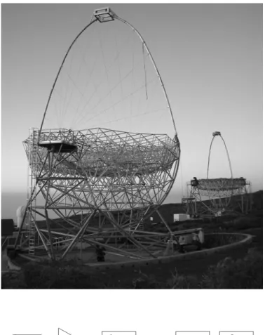
HE MAGIC telescope is a new and innovative instrument dedicated to the detection of High Energy (HE) and Very High Energy (VHE) gamma-rays (E>30 GeV) from astrophysical sources [1], [2]. The telescope (see Fig. 1) is located at the “Roque de los Muchachos” Observatory, on the Canary Island of La Palma (Spain), and makes use of the well established Imaging Atmospheric Cherenkov technique to detect the highest energy photons from the Universe. The MAGIC Collaboration decided to build (2005 / 2006) a second telescope, on the same site, at 85 m distance from the first one. Some of the features of this new telescope will be [3]:
• Advanced photosensors with higher sensitivity and better time response, able to detect ns pulses
• Increased camera area instrumented with small-size pixels, which enhances the spatial resolution with respect to the original camera.
1 Dpto. Física Aplicada III, Universidad Complutense de Madrid, Av.
Complutense s/n 28020 Madrid, SPAIN (e-mail: antoranz@gae.ucm.es).
2 Dpto. Física Atómica, Molecular y Nuclear, Universidad Complutense de Madrid, Av. Complutense s/n 28020 Madrid, SPAIN.
3 Full list of authors is at http://magic.mppmu.mpg.de
• Mirror elements with larger surface and improved non- interfering mirror adjustment.
• Digital signal readout with improved time resolution for sub ns range signal processing.
• Ability to operate either in individual or stereo mode with MAGIC I.
Fig 1. Onsite picture of MAGIC I and II Telescopes (top). The structure of MAGIC II is ready, and the electronics are under development. Single pixel structure in MAGIC I (bottom).
The MAGIC II camera design is based in a pixel chain
T
2 where the signal is first detected by a state of the art
photomultiplier tube (PMT). The PMT output is connected to a microwave preamplifier stage, which feeds a Vertical Cavity Surface Emitting Laser (VCSEL). This laser transmits the signal through an optical fiber to the data adquisition and processing system, located nearby the base of the telescope.
This pixel structure is shown in Fig. 2.
In order to take advantage of the bandwidth features of the VCSELs and the new PMTs, it is necessary to design a preamplifier stage able to rise the signal levels up to the voltages demanded by the VCSEL, with bandwidths of around 1 GHz.
II. SOFTWARE OVERVIEW
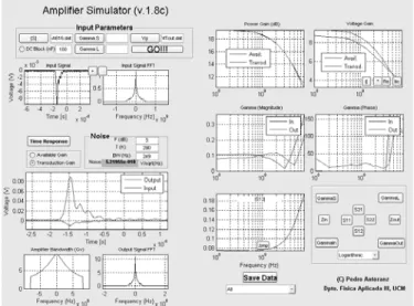
Software based on MATLAB has been developed to simulate the amplifier output in the time domain. It features the ability to accurately reproduce the pulse shape including mismatch effects and noise pollution.
Fig. 2. User interface of the simulation program. The rightmost part shows the amplifier characteristics, and the leftmost the time domain response.
The program makes use of the amplifier and photosensor measured parameters. With a vectorial network analyzer, the scattering matrix (S) of the amplifier and the reflection coefficient (Γ) of the photosensor are measured in the frequency domain. The sampled input signal can be either measured in the time domain with a digitizing oscilloscope or in the frequency domain with a spectrum analyzer.
The analytic part of the software provides information about the main amplifier characteristics, as the available and transducer gains in terms of either voltage or power signals, or the input and output impedances. The analytical expressions for these gains were obtained by using the Mason’s Rule and signal flow graph theory shown in Fig. 3.
Fig. 3. Schematics of the amplifier with the source and load impedances represented by their reflection coefficients (top) and flow graph used to apply the Mason rule (bottom).
The flow graph theory is regularly used to calculate the ratio between either two voltages or currents at the nodes or branches of a high frequency circuit [4]. The main interests of this theory lies in the fact that it provides direct information on reflection losses at any circuit port. It also facilitates the calculation of voltage or current gains by giving analytical expressions for them in terms of magnitudes that can easily be measured at high frequencies, such as the own S parameters and the reflection coefficients. This enables a convenient unification of the low frequency formalism, based on voltage and currents, and the high frequency one, based on waves.
The influence of the mismatches between the photosensor and the amplifier input was investigated. Fig. 4(a) illustrates an example were these effects can be observed: the mismatch was simulated by means of a RC load and the S parameters of a standard pulse amplifier.
6 8 10 12 14 16
0,0 0,2 0,4
6 8 10 12 14 16
0,00 0,04 0,08
Mismatched output Matched output Input
Voltage [V]
Time [ns]
Voltage [V]
Input 1 GHz 300 MHz 100 MHz 3 dB Bandwidth
Fig. 4. (a) Effect of the source mismatch on the amplifier output signal. (b) Effect of the amplifier bandwidth on the distortion of the output pulse.
The effects of the limitations in the amplifier bandwidth on
3 the pulse distortion were also simulated. Fig. 4(b) shows the
output signal for different bandwidths. The amplitudes were normalized to the input pulse to better appreciate the amplifier distortion.
III. FEATURES OF NEW PREAMPLIFIERS
A preamplifier stage based on Silicon-Germanium (SiGe) Monolithic Microwave Integrated Circuit (MMIC) technology [5] has been designed, fabricated and tested. All the components are mounted on microstrip lines with standard FR4 board. The dielectric permittivity of this material is fairly high (4.2) and as a result small size and efficient field confinement is obtained.
Once the amplifier is designed and fabricated, the scattering matrix is measured by means of the vectorial network analyzer and the amplifier parameters are obtained. The power losses can be calculated as [6]
2 22
2 11
1 1
S PL
S PL
out in
−
=
−
=
(1)
Fig. 5. shows the gain and the power losses of the 50 Ω matched amplifier as a function of the frequency. This configuration gives a 3 dB bandwidth in excess of 1 GHz, with a power gain close to 18 dB. The losses due to reflection at the input are lower than 10% of the total incident power for frequencies below 1 GHz.
The design of the bias network is particularly critical.
Typical networks allow the pass of intermediate frequencies to the DC source, and this produces a strong pulse distortion at the amplifier output. In order to avoid this effect a bias network based on SMD RLC filter with a very low cut-off frequency has been designed. Two blocking capacitors are used: one at the input that blocks the photosensor DC current, and another at the output that avoids the DC bias current to reach the device connected to the amplifier.
Fig. 5. Power gain and power losses of a 50 Ω matched amplifier.
In addition, special attention needs to be paid to grounding.
In order to avoid distributed effects it is necessary to make use of multiple via holes at both sides of the main transmission line.
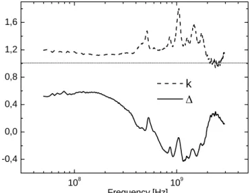
The k-∆ stability test [7], [8] has been applied to the amplifier, where ∆ is the determinant of the S matrix and
21 12
2 2 22 2 11
2 1
S S
S
k − S − + ∆
= (2)
This test has shown that the device is unconditionally stable up to 2 GHz, as it can be observed in Fig. 6. A loss of unconditional stability is obtained at 2.1 GHz. However, no relevant power content in this frequency is found in the spectra of the typical signals to be handled by the amplifier under real world conditions, and therefore no oscillations are expected at any of the measured frequencies.
The ringing observed in the pulse is due to the inductances in the last two dynodes of the photomuliplier, and can be reduced by adding 50 Ω resistors in the connection of these dynodes. This ringing proves that the time domain resolution of the amplifier is enough to distinguish between two short adjacent pulses.
108 109
-0,4 0,0 0,4 0,8 1,2 1,6
k ∆
Frequency [Hz]
Fig. 6. k-∆ stability test made with the measured S parameters of the prototype.
108 109
0 20 40 60 80 100
0 2 4 6 8 10 12 14 16 18 20
Input Power Loss Output Power Loss
Power Loss [%]
Frequency [Hz]
Power Gain [dB]
Power Gain
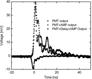
The amplifiers were tested with a PMT illuminated by a picosecond-pulse blue laser able to generate pulses with effective widths of 2 nanoseconds. The response of the system is shown in Fig. 7, as measured by a digital storage oscilloscope (DSO) with 6 GHz bandwidth. The PMT output signal was first monitored (star symbols in the figure).
When the signal was applied directly to the amplifier, the response shown by the circles was observed. Then a delay line of 10 ns was inserted between the PMT and the amplifier, leading to the pulse labelled as ‘PMT + Delay + AMP Output’. Only in this last case the effect of the standing waves generated by mismatches between these two devices became
4 evident, with the monitoring of a secondary pulse with an
exact delay of 10 ns.
Fig. 7. Pulses measured at the input and at the output of the amplifier. The addition of a transmission line between the source and the amplifier produces secondary pulses due the delay in the reflected signal.
IV. CONCLUDING REMARKS
A MATLAB based program has been developed to simulate pulse distortion, delay and voltage losses due to mismatches between photodetectors and input pulse amplifiers. This program makes use of input data that can easily be measured in a laboratory with conventional microwave instrumentation.
The simulations performed with the software presented in this work have illustrated the relevance of mismatch effects in the detection of ns range pulses using PMTs. By simulating the PMT with an RC load and using a standard pulse amplifier, voltage losses of more than 30% were observed.
Although here we present results with a PMT, the program has a fairly broad range of application and will be helpful in future upgrades of both MAGIC I and II cameras, where other photodetectors such as Silicon PMTs or Hybrid photodetectors (HPDs) are presently under investigation.
The problem of mismatches has successfully been solved with the design of an integrated pulse amplifier based on a SiGe MMIC. The amplifier features usable gain of more than 12 dB up to 3 GHz and the measurements made with it have shown its ability of amplifying ns range pulses without noticeable distortion or ringing when the amplifier is connected immediately after the PMT. Secondary pulses due to mismatch can only be observed when a delay line is placed between the source and the amplifier, but this situation will not occur in the camera. The software presented here was a valuable tool to predict the output signal distortion effects of mismatches.
V. REFERENCES
[1] E. Lorenz, “Ground-Based Gamma-Ray Astronomy”, Acta Physica Polonica B 35 (2004), 1991-2006.
-20 0 20 40
-10 0 10 20 30 40
PMT output PMT+AMP output PMT+Delay+AMP Output
Voltage [mV]
Time [ns]
[2] D. Ferenc for the MAGIC collaboration, “The MAGIC gamma-ray observatory”, Nuclear Instruments and Methods A 553 (2005), 274-281.
[3] http://magic.mppmu.mpg.de
[4] S. J. Mason, “Feedback theory - Further properties of signal flow graphs”, Proc. IRE 44 (1956), 920-926.
[5] Infineon Technologies, “BGA616 Datasheet”, (2001).
[6] G. Gonzalez, “Microwave Transistor Amplifiers Analysis and Design”, Prentice Hall (1984).
[7] J. M. Rollett, “Stability and power gain invariants of linear two-ports”, IRE Trans. Circuit Theory, vol. 9 num. 3 (1962), 29–32.
[8] D. Woods, “Reappraisal of the unconditional stability criteria for active 2-port networks in terms of S parameters”, IEEE Trans. Circuits Syst., vol. 23, (1976) 73–81.