Lecture 3: Asynchronous Input Signals
G. Kemnitz ∗ , TU Clausthal, Institute of Computer Science May 8, 2012
Asynchronous input signals, at the test board the signals from the switches and buttons, has to be sampled before internal processing with a clock period larger than the de-bouncing time (see [1], section 1.5). The following exercises introduce step by step the design of a sequential circuit with asynchronous inputs from switches and buttons.
1 Examination of the bouncing of a switch with the logic analyzer
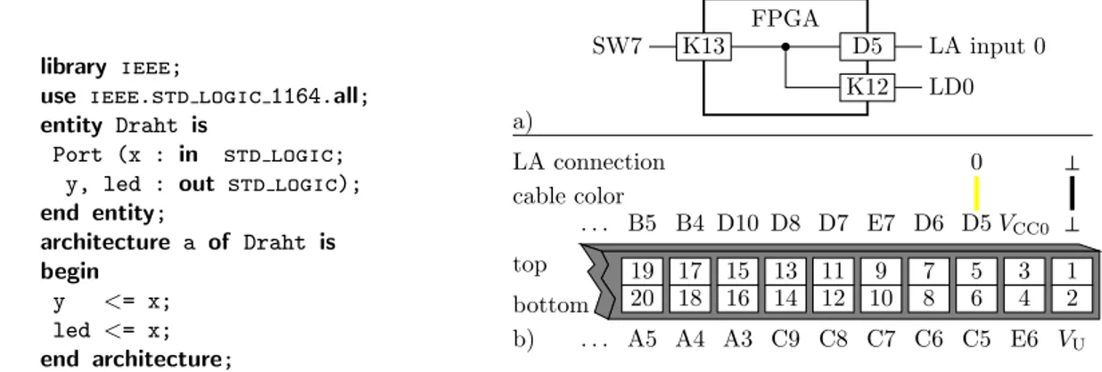
Program the FPGA so that the switch input
SW0
on the test board is connected via the FPGA with LED
LD0
and pin 5 of expansion connector
A2
(LOC D5) (figure 1 a). Connect the logic analyzer as shown in figure 1 b and record the waveform during turning the switch on several times (Settings for the logic analyzer: 1.500.000 samples per second, trigger on first rising edge of the signal). How long is the maximum observed bouncing time? By which power of two the 50 MHz clock should be divided to sample the switching signal?
0 cable color
LA connection
V
CC0V
UD5 D6 E7 D7 D8 D10 B4 B5
E6 C5 C6 C7 C8 C9 A3 A4 A5
1 2 3 4 5 6 7 8 9 10 11 12 13 14 15 16 17 18 19 20 . . . . . .
D5 K12 FPGA
LD0
SW7 LA input 0
bottom b) top a) library ieee ; K13
use ieee.std logic 1164.all;
entity Draht is
Port (x : in std logic ; y, led : out std logic );
end entity;
architecture a of Draht is begin
y <= x;
led <= x;
end architecture;
Figure 1: a) Circuit for exercise 1 b) Connection of the logic analyzer to the expansion connector
A2
(Draht – engl. wire)
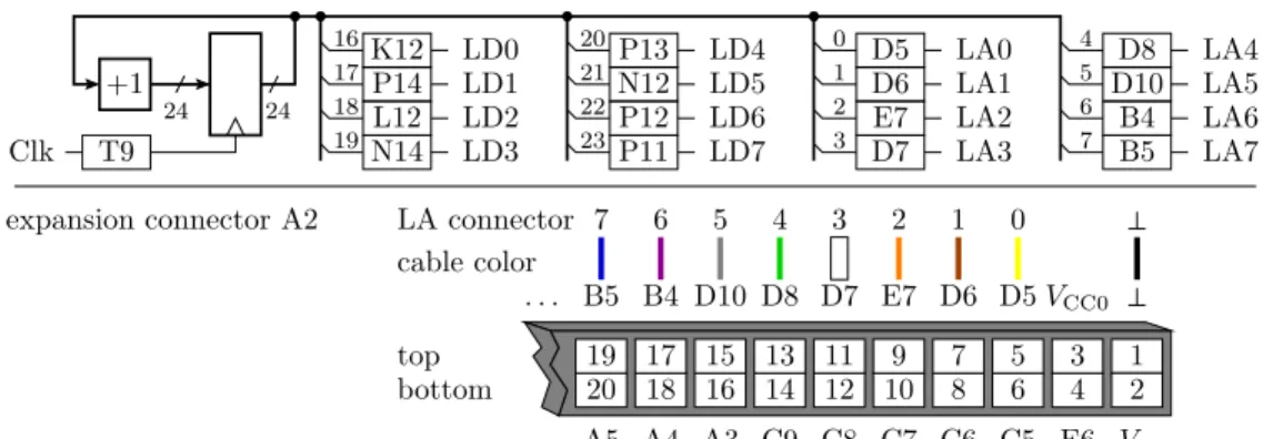
2 Counting the signal edges during bouncing
For this experiment the sequential circuit in figure 2 a has to be described in VHDL and pro- grammed in the FPGA. The switching signal is sampled by a shift register of length two. If both values differ the counter state is increased by one. The counter state is displayed on the LEDs.
∗