Probing spin helical surface states in topological HgTe nanowires
J. Ziegler,1R. Kozlovsky,2C. Gorini,2M.-H. Liu (),2,3S. Weishäupl,1H. Maier,1R. Fischer,1D. A. Kozlov,4,5 Z. D. Kvon,4,5N. Mikhailov,4S. A. Dvoretsky,4K. Richter,2and D. Weiss1,*
1Institut für Experimentelle und Angewandte Physik, Universität Regensburg, 93040 Regensburg, Germany
2Institut für Theoretische Physik, Universität Regensburg, 93040 Regensburg, Germany
3Department of Physics, National Cheng Kung University, Tainan 70101, Taiwan
4A.V. Rzhanov Institute of Semiconductor Physics, Novosibirsk 630090, Russia
5Novosibirsk State University, Novosibirsk 630090, Russia
(Received 25 August 2017; revised manuscript received 4 December 2017; published 29 January 2018) Nanowires with helical surface states represent key prerequisites for observing and exploiting phase- coherent topological conductance phenomena, such as spin-momentum locked quantum transport or topological superconductivity. We demonstrate in a joint experimental and theoretical study that gated nanowires fabricated from high-mobility strained HgTe, known as a bulk topological insulator, indeed preserve the topological nature of the surface states, that moreover extend phase-coherently across the entire wire geometry. The phase-coherence lengths are enhanced up to 5μm when tuning the wires into the bulk gap, so as to single out topological transport. The nanowires exhibit distinct conductance oscillations, both as a function of the flux due to an axial magnetic field and of a gate voltage. The observedh/e-periodic Aharonov-Bohm-type modulations indicate surface-mediated quasiballistic transport. Furthermore, an in-depth analysis of the scaling of the observed gate-dependent conductance oscillations reveals the topological nature of these surface states. To this end we combined numerical tight-binding calculations of the quantum magnetoconductance with simulations of the electrostatics, accounting for the gate-induced inhomogeneous charge carrier densities around the wires. We find that helical transport prevails even for strongly inhomogeneous gating and is governed by flux-sensitive high-angular momentum surface states that extend around the entire wire circumference.
DOI:10.1103/PhysRevB.97.035157
I. INTRODUCTION
Three-dimensional topological insulators (3DTIs) are a par- ticular class of bulk insulators hosting time reversal symmetry- protected metallic surface states. The latter are helical, i.e., characterized by (pseudo)spin-momentum locking and de- scribed by low-energy effective Dirac-type models [1]. In nanowires based on 3DTI materials such locking heavily affects the one-dimensional (1D) subband spectrum and, if combined with superconductivity, is a basic ingredient for the realization of Majorana modes [1,2]. Moreover, from a general quantum transport perspective, 3DTI nanowires provide a particularly rich playground due to the interplay between topological properties and effects arising from phase coherence. The fact that the conducting states are “wrapped”
around an insulating bulk, in conjunction with their helical nature, leads to various interesting and geometry-sensitive magnetoresistive phenomena [2,3] that are inaccessible in stan- dard metallic systems, whose bulk and surface contributions cannot in general be singled out.
*Corresponding author: dieter.weiss@ur.de
Published by the American Physical Society under the terms of the Creative Commons Attribution 4.0 International license. Further distribution of this work must maintain attribution to the author(s) and the published article’s title, journal citation, and DOI.
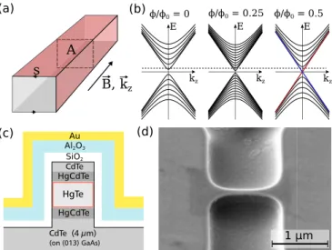
In particular, a 3DTI nanowire in a coaxial magnetic field with magnitudeB and associated fluxφ=AB, as sketched in Fig. 1(a), is expected to show peculiar Aharonov-Bohm type magnetoresistance features. Indeed, oscillations with a period of one flux quantum φ0 =h/e (where h=2πh¯ is Planck’s constant andethe elementary charge) were observed in early experiments [4,5]. According to theory [2,6–9] these oscillations reflect the wire’s 1D subband structure, given by
E= ±hv¯ F
kz2+kl2 with kl =2π P
l+1
2 − φ φ0
. (1)
In Eq. (1),vFis the Fermi velocity of the surface carriers,kz
the coaxial, andklthe transversal wave vector, the latter having the meaning of angular momentum. The angular momentum quantum number is labeled byl∈Zand its half-integer shift in kl is caused by a curvature induced Berry phase. The resulting energy spectrum is sketched in Fig.1(b)for three characteristic values of the magnetic flux. Forφ=0 an energy gap is present (due to the Berry phase) and the 1D subbands are twofold degenerate with respect to angular momentum. Note, however, that owing to their Dirac-like nature these states are not spin degenerate. For finite flux such asφ/φ0 =0.25 the degeneracies with respect toklare lifted. Forφ/φ0 =0.5, the magnetic flux cancels the Berry phase and the l=0 states become gapless,kl=0=0. This linear gapless state is nonde- generate. More generally, the total number of states is odd, and time-reversal symmetry, restored atφ/φ0 =0.5, implies one
FIG. 1. HgTe-based nanowire. (a) Sketch of a nanowire with cross sectionAand magnetic fieldB along the wire axis. (b) 1D band structures of the surface states of three-dimensional topological insulator nanowires for three different representative magnetic fluxes.
(c) Schematic cross section of a nanowire employed in experiment.
The nanowires are etched from wafers containing an 80 nm strained HgTe film and consist of a 4 µm CdTe base layer grown on (013) GaAs substrate, two 20 nm Hg0.7Cd0.3Te buffer layers on top and bottom of the HgTe and a 40 nm CdTe cap layer. After wet chemical etching the wire is covered by SiO2/Al2O3and a metallic top gate. (d) SEM micrograph of a representative HgTe TI nanowire, taken at a tilt angle of 50° before deposition of the topgate structure. It has a length of 1.3 µm and a median width of 163 nm.
“perfectly transmitted mode” [10]. Forφ/φ0 =1 the spectrum recovers itsφ/φ0=0 form. Further increasing the flux leads to analogous cycles: The Berry phase cancellation, and thus the appearance of a gapless state, takes place for half-integer values ofφ/φ0, wheneverkl =0 for a givenl, while for integer values the gapped spectrum forφ=0 in Fig.1(b)is recovered.
This “shifting” of the 1D subbands with changing flux implies that for a given Fermi level position the conductance should be φ0 periodic. Dominating h/e oscillations were indeed observed in a number of experiments [11–17]. Fur- thermore, the phase of the Aharonov-Bohm-type oscillations depends on the Fermi level position. To be definite, consider EF close to zero: No states are present for φ=0 (and corresponding even multiples ofφ0/2), whereas forφ/φ0= 0.5 (and corresponding odd multiples of φ0/2) the gapless mode emerges. Hence, one expects a conductance minimum (maximum) for integer (half-integer) flux quanta. For EF slightly above zero, e.g., at the dashed line in Fig. 1(b), the situation is reversed: Two modes are present forφ=0, and only one forφ/φ0=0.5. Such π-phase shifts as a function of the Fermi level position, i.e., the gate voltage Vg, were observed in Bi1.33Sb0.67Se3[15] and Bi2Te3[16]. If the Fermi level can be tuned to the Dirac point a conductance minimum for φ/φ0=0 and a maximum at φ/φ0=0.5, as observed in Ref. [15], are signatures of the Berry phase of π and thus of spin-helical Dirac states. However, in strained HgTe nanowires investigated here, the Dirac point is buried in the valence band [18–20] and thus cannot be singled out and probed on its own. Without direct access to the latter, the phase
switching alone is not an exclusive signature of Dirac states:
The 1D subband spectrum of trivial surface states, and thus the resulting conductance, would also beφ0periodic.
Hence the crucial question arises how to distinguish topo- logical from trivial states in 3DTI nanowires with an inacces- sible Dirac point, such as strained HgTe. This is the central point that we address below, by quantitatively analyzing the conductance oscillation periodicity occurring as a function of gate voltage Vg at fixed flux. The observed oscillations reflect directly the 1D subband structure and its degeneracies.
This allows us to draw conclusions about the nature of the surface states, trivial ones being spin degenerate, in contrast to spin-helical Dirac states. In doing so, we also address a second issue, namely the consequences of a varying carrier density around the wire circumference. Experiments typically rely on the use of top and/or back gates, which couple differently to the top, bottom, and side surfaces of the 3DTI wires. The carrier density (or the capacitance) therefore becomes a strongly varying function of the circumference coordinates. Note also that a certain degree of inhomogeneity is expected even in the absence of gating, as a consequence of intrinsic system anisotropies [21]. As we show below, an inhomogeneous surface charge distribution modifies significantly the band structure, yet leaves the essential physics intact.
II. NANOWIRE DEVICES
The investigated TI nanowires were fabricated from (013) oriented, strained 80-nm-thick HgTe thin films grown by molecular beam epitaxy on (013) oriented GaAs substrates (for details see Ref. [22]). A cross section through the layer sequence is shown in Fig.1(c). Using electron beam lithogra- phy and wet chemical etching, nanowires as the one shown in Fig.1(d)were fabricated. For etching we used a Br2-based wet etch process to preserve the high charge carrier mobilities of the bulk material. The wet etching did not result in perfectly rectangular wire cross sections but rather in trapezoidal ones with the narrower side on top. In Fig. 1(d) the top width of the wire’s central segment was 133 nm while the bottom width was 193 nm, resulting in an average (median) width of 163 nm. For easier modeling below we use a rectangular cross section with area A given by the average wire width times HgTe film thickness,A=wh. This approximation reduces the circumferenceP that determines the spacing between angular momenta, kl=2π/P, by 2–3%. As discussed below, the resulting effect of this assumption is negligible. After etching the wires were covered with 30 nm of Si2O3 using plasma enhanced chemical vapor deposition and 100 nm Al2O3 de- posited with atomic layer deposition. For gating a metallic top layer consisting of titanium and gold was used. The resulting schematic cross section is depicted in Fig.1(c) and will be used for the electrostatic modeling in Sec.IV. Ohmic contacts to the wire were formed via soldered indium. The nanowires were fabricated in both a true four-terminal geometry (devices denoted by w3-w5) as well as a quasi-two-terminal geometry (devices t1-3, w1-2). In the latter case, the nanowire constric- tion was embedded in a larger Hall bar, where the voltage probes are several µm removed from the device.
The magnetoconductance of the wires was measured in a dilution refrigerator at temperatures of typically 50 mK and
TABLE I. Geometrical parameters of the nanowire structures considered. The heighthof all devices is given by the 80-nm-thick HgTe layer of the wafers. Median width and length of the structures are denoted bywandl, respectively. The circumferenceP and the expected period forh/eoscillationsBh/e(in Tesla) were calculated assuming the surface state wave functions to be located∼5 nm beneath the bulk surface.
Device w(nm) l(µm) P (nm) Bh/e(T)
t1 302 0.99 724 0.203
t2 518 2.06 1156 0.116
t3 246 2.51 613 0.249
w1 310 1.33 740 0.197
w2 163 1.33 446 0.386
w3 178 1.06 476 0.351
w4 294 1.95 708 0.208
w5 287 2.97 694 0.212
magnetic fields up to 5 T. A rotating sample holder was used for measurements to allow for in- and out-of-plane alignment of the magnetic field. Standard AC lock-in techniques and Femto voltage preamplifiers were used at excitation amplitudes and frequencies of typically 1–15 nA and 7–13 Hz, respectively.
Additionally, a cold RC filter was added to suppress noise at the top gate and to improve reproducibility of magnetotransport traces. In the following, we present results from a total of eight nanowires. Parameters defining their geometries are listed in TableI. Devices t1-t3 were investigated regarding the tempera- ture dependence of the Aharonov-Bohm-type oscillations (see Sec.III A), while devices w1-w5 were studied with regard to signatures of the subband structure (see Sec.III B).
III. CHARACTERIZATION OF CONDUCTANCE OSCILLATIONS
A. Magnetoconductance
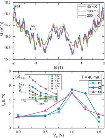
Figure2(a)shows the measured two-point conductanceG as a function of a magnetic fieldBapplied along the wire axis.
The experimental data was taken at temperaturesT between 40 mK and 300 mK. An overall h/e periodicity is clearly visible, as indicated by the horizontal bar in Fig. 2(a) (and analyzed in more detail below). The fact thatG(B) exhibits Aharonov-Bohm-type h/e periodicity instead of h/(2e) be- havior, arising from interference between time-reversed paths in the diffusive limit [24], implies that transport along the wires is indeed nondiffusive, i.e., the elastic mean free path is presumably not much shorter than the wire length and larger than the wire circumference. However, the additional conductance fluctuations present inG(B) in Fig.2(a)indicate residual disorder scattering.
From the temperature dependence we can estimate the phase coherence length lϕ by using the exponential decay of the amplitudeGof theh/econductance oscillations for ballistic transport on scales of the perimeterP [25],
G∝exp
− P lϕ(T)
. (2)
In Fig. 2(b) the resulting phase coherence lengths obtained from three devices are plotted as a function of Vg. For all samples minimal values of 1 µm to 2 µm are found forlϕ, while
FIG. 2. (a) Magnetoconductance oscillations of device t1 mea- sured at different temperatures T. The traces show h/e-periodic oscillations with amplitudesG(T) decreasing with increasing tem- peratureT. TheT dependence of the amplitude of sample t1, taken at various gate voltages, is shown in the inset of panel (b), along with the corresponding fits using Eq. (2). The exponential fits allow for the extraction oflϕ, displayed in panel (b) as a function of gate voltage Vgfor devices t1-t3.
maximal values reach 5 µm at gate voltages aroundVg =1 V.
AtVg=1 V the Fermi levelEFis in the bulk gap, as extracted from independent measurements for macroscopic Hall bars made from the the same material [23,26]. ForEF in the gap the phase coherence lengths of the topological surface states are expected to be largest as backscattering is reduced and scattering into bulk states is suppressed.
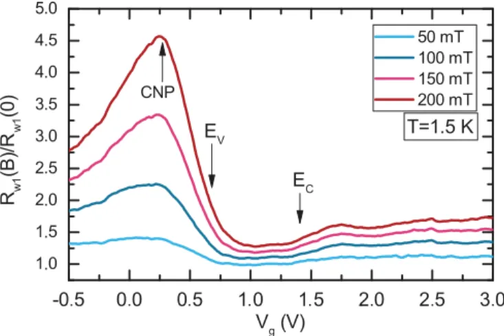
Figure3showsVg-dependent resistance traces of device w1 for a number of magnetic fieldsB normalized to their value atB=0. The maximum of the longitudinal resistance, which comes out more clearly with higher magnetic fields, is usually ascribed to the charge neutrality point (CNP). In strained HgTe it is located slightly in the valence band [23]. Hence the valence band edge is located on the right hand side of the maximum.
TheVg locations of the conduction and valence band edges, indicated by arrows in Fig.3, have been obtained by comparing to the results described by Kozlovet al.(2014) [23,26].
Next we study in more detail the Aharonov-Bohm-type oscillations and in particular theirVg dependence, here rep- resentatively discussed for device w1. To this end, we remove the small hysteresis of the superconducting magnet from the conductance and subtract a smoothly varying background
FIG. 3. Normalized longitudinal resistanceRw1(B)/Rw1(B=0) as a function of gate voltage for nanowire device w1. The upper and lower bounds of the bulk band gap are indicated by arrows and were determined by comparing to analysis done on material with the same wafer stack by Kozlovet al.[23].
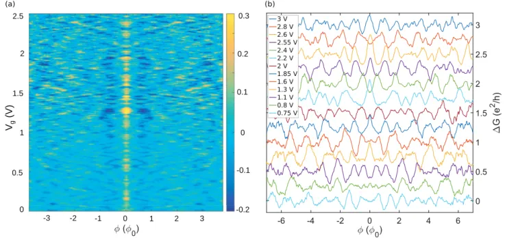
Gsm(B) using a Savitzky-Golay filter [27]. The filter was applied in a way that frequencies smaller than 1/2φ0 are cut off. The resulting conductanceG(Vg;φ) is shown in the color plot in Fig.4(a). Here, the gate voltage spacing of neighboring traces isVg =0.01 V. Corresponding data, but now as line cuts taken at different values of Vg are shown in Fig. 4(b) for sample w2.Gshows dominantφ0-periodic oscillations over a large gate voltage range, as well as a pronounced phase switching between minima and maxima, i.e., additional conductance oscillations upon varyingVg at fixed flux (to be analyzed in Sec.III B). Theφ0periodicity is confirmed by a fast Fourier transform (FFT) analysis of traces covering a magnetic field range corresponding to 20φ0in the case of device w1. As the period of the oscillations should be independent of the gate voltage an average of the FFTs was taken in the voltage range 0 to 3 V. TheVg-averaged FFT is shown in Fig.5as a function of 1/φ. Here, we used the square geometry with a median width of 310 nm for w1 and assumed that the topological surface states are 5 nm below the surface to compute the magnetic flux φ=ABfromB. The resulting FFT peak is located at 0.87/φ0. The peak falls into the expected region of anh/esignal, where the lower bound is given by the geometrical dimensions of the nanowire cross section as listed in TableI. The upper bound is calculated for the case where the wave function of the surface states lies 8 nm within the TI bulk. To conclude, the distinct peak of the FFT close to 1/φ0implies that, at low temperatures, transport is mediated by states extending phase-coherently across the entire surface of the weakly disordered nanowire.
B. Subband-induced conductance modulation
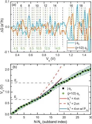
The detection of the Aharonov-Bohm oscillations that switch their phase as a function ofVg is by itself insufficient to confirm the topological nature of the underlying surface states. Therefore we have to go beyond previous analysis and aim at a quantitative description of theG(Vg) oscillations, which directly reflect the subband structure of the quasi-1D wires. G(Vg;φ) is extracted from line cuts taken at half integer and integer values ofφ/φ0in Fig.4(a)and plotted as
blue, respectively, orange curves in Fig.6(a). To suppress the influence of aperiodic conductance fluctuations we averaged over all positive and negative integer multiples ofφ0 in the dataset, i.e., ±φ0, ±2φ0, and ±3φ0 to generate the orange curve in the case of the representative device w1. Accord- ingly, the blue curve results from an average over positive and negative half-integer multiples calculated from±0.5φ0,
±1.5φ0, and±2.5φ0. The line cut forφ=0 was omitted due to a large weak antilocalizationlike background profile that renders background removal difficult. In Fig. 6(a) the two conductance curvesG(Vg) obtained in this manner exhibit antiphase oscillations as a function of Vg, i.e., maxima of G(Vg) for integer multiples ofφ0go along with minima of G(Vg) for half integer multiples.
In Secs.IV–VIwe carry out an in-depth analysis associating these characteristics with the quantized subbands of helical surface states. Based on this study the analysis of the conduc- tance oscillations in Fig.6(a)proceeds as follows: The minima inG(Vg) correspond to a Fermi level at the edge of a subband since the corresponding high density of states (the van-Hove singularity) causes enhanced scattering. Accordingly, the gate voltage distance Vg between two minima, corresponding to the period of the conductance oscillation, can be directly mapped onto the subband spacing. One key property that distinguishes topological surface states from their trivial coun- terparts is their degree of spin degeneracy. It directly affects Vgsince a spin degeneracy of two, as for trivial surface states, implies that twice as many states need be filled compared to helical edge states. This allows us to extract the spin degeneracy of the subbands involved by quantitatively analyzing the distanceVg between adjacent conductance minima.
To increase the accuracy of the extractedVg, we use the anticorrelation between the two curves forj φ0and (j+0.5)φ0 withj = ±1,±2,...and the corresponding minima-maxima pairs in order to label the pairs by a running index and to obtain Vg. Pairs with the maximum corresponding to integer/half- integer flux quantum are labeled by an integer/half-integer index by black and green dashed lines, respectively. Since in strained HgTe the Dirac point is located in the valence band, we do not know the precise number of filled 1D subbands at a given gate voltage. We thus start counting by fixing a reference voltageV0at which a certain (unknown) numberN0 of subbands is filled and use the relative indexN−N0, with Nthe total number of occupied subbands. In Fig.6(b)the gate voltage at which a particular minimum-maximum pair occurs is plotted as a function of the corresponding indexN−N0.
The connection betweenG(Vg;φ) and the nanowire band structure isa priori not obvious, since the nanowire surface charge carrier density, and ergo its capacitance, is inhomoge- neous due to asymmetric gating. However, as we will detail in Secs.IV–VI, an analysis in terms of asingleeffective charge carrier densityneff, i.e., effective capacitanceCeff, turns out to be fully justified. They are related to each other via
(neff−n0)e=Ceff(Vg−V0), (3) whereV0is the gate voltage at which the oscillation counting starts andn0the corresponding carrier density. For a 2D system the Fermi wave vectorkF is given by
kF =
(4π/gs)neff (4)
FIG. 4. Quantum conductance corrections of transport measurements in TI nanowires. (a) Color plot of conductance correctionGas a function of magnetic fluxφ(in units of flux quantumφ0) and gate voltageVgfrom device w1. (b) Selection of representative magnetoconductance curves from device w2 comprising a larger flux range. The different traces (offset for clarity) exhibit clearφ0-periodic behavior, as well as a switching of the phase with varyingVg.
with the spin degeneracy factorgs =1 and gs =2 for spin- resolved topological surface states and spin-degenerate trivial surface states, respectively. Assuming a constant subband split- tingE/( ¯hvF)=kl=2π/P [in view of Eq. (1)], the Fermi wave vector at a conductance minimum (subband opening) can be written as
kF =k0+(N−N0)kl with k0 =
(4π/gs)n0. (5) Combining Eqs. (3), (4), and (5) yields the relation
Vg−V0= gse 4π Ceff
2k0(N−N0)kl+(N−N0)2kl2 (6)
FIG. 5. Fourier spectrum of nanowire magnetoconductance oscil- lations. Fast Fourier transform, calculated from the magnetoconduc- tance of device w1 and averaged over allVgvalues, shows a dominant peak close to 1/φ0, reflectingφ0=h/e-periodic oscillations. The bar at the peak denotes the expected range of the peak to occur, see text.
between gate voltage and subband level indexN. The distance between two conductance minima depends essentially on the effective capacitanceCeff and wire circumferenceP.
Equation (6) is only valid for Vg values for whichEF is located in the bulk gap. We estimate thisVg range from the gate-voltage dependent resistance curves plotted in Fig.3. The corresponding region is highlighted by the dashed horizontal lines in Fig.6(b) and matches the region of longest phase- coherence lengthslφdiscussed above.
The key quantity which is missing for comparing Eq. (6) with the experimental data of Fig.6(b)is the effective capac- itanceCeff, which is not directly accessible from experiment.
Therefore, we resort to a numerical solution of the Poisson equation (described in Sec.IV) and the definition ofCeffgiven in Sec. V C. The anticipated result of such a calculation is Ceff =3.987×10⁻⁴ F/m2, carried out for the geometry and dielectric constants of the present wire. The curves obtained from Eq. (6) both for spin helical and trivial surface states are shown in Fig.6(b). In the gap region the experimental data points are best described by the model invoking spin-helical surface states (solid lines); trivial surface states lead to a steeper slope (red dashed line) and fail to describe the experiment. It would be interesting to apply this kind of analysis to wires with trivial surface states [28].
The analysis described in this section was carried out for five devices with different cross sectionsA. For each device the nanowire circumferenceP, which defines the subband splitting kl=2π/P, was extracted from the SEM micrographs. Al- ternatively, one can extract the circumference by fitting the data points, shown for samples w1-w5 in the inset of Fig.7, with Eq. (6). Using the corresponding effective capacitancesCeff, the only remaining fit parameter iskl,fit. The best fits in the relevantVgranges for all five investigated samples are shown
FIG. 6. (a) Conductance oscillations due to subband quantization.
Conductance correctionsGas a function of gate voltage for integer (blue curve) and half-integer (orange curve) values ofφ/φ0, obtained by averaging several line cuts taken along constantφfrom the data set of device w1 in Fig.4(a). The curves exhibit a clear anticorrelated behavior. Each minimum-maximum pair (marked by vertical dashed lines) is assigned an indexNthat can be associated with a subband of the wire, see text. (b) Gate voltage position of conductance maxima from (a) as a function of (subband) indexN (with arbitrary offset N0). Within the bulk gap (marked by dashed horizontal lines) the red curve segments denote expected behavior forVg(N) based on models for helical Dirac-type (solid line) and trivial spin-degenerate (dashed) surface states, see main text. Agreement of the conductance data with the former model implies the topological character of the surface states. For comparison, the blue line shows corresponding results for a Dirac surface state model, based on a trapezoidal cross section instead of a simple rectangular cross section. The gray area around the data points is obtained repeating the analysis while introducing an artificial error of up to±0.2 inφ0, showing that the method is robust against errors inφ0.
in the inset of Fig.7. In the main panel of Fig.7the extracted values of kl,fit are plotted versuskl. The plot shows that kl≈kl,fit within experimental accuracy, thus confirming the suitability of the analysis. In the following we present an in-depth study of the nanowire electrostatics, band structure, and magnetoconductance that provides the theoretical basis for the analysis of Fig.6 indicating the existence of helical surfaces states.
FIG. 7. Analysis of subband spacing. The inset shows the de- pendenciesVg(N−N0) of samples w1-w5. The black dashed lines are best fits (within the bulk band gap) based on Eq. (6) withkl
as the only fit parameter. Main panel: Best fitting valueskl,fit of samples w1-w5 are plotted versuskl =2π/P, determined from the nanowires’ circumferenceP taken from SEM micrographs. The dashed straight line marks the conditionkl=kl,fit. Devices whose data is presented in this paper are marked by squares.
IV. ELECTROSTATICS OF WIRE GEOMETRY Since the capacitance used in the preceding section is not experimentally accessible we need to resort to numerical analysis. Furthermore, in the experimental setup, the Fermi energy is locally tuned by a gate electrode that covers roughly the upper part of the nanowire [see Fig.1(c)] and induces a nonuniform surface electron density n(z,s), where z is the longitudinal (0< z < L) andsthe circumferential coordinate (0< s < P =2w+2h). To account for the inhomogeneous charge density in our subsequent transport simulations while keeping the model as simple as possible, we assume that n(z,s)=n(s) is constant along the z direction. We imple- mented the finite-element based partial-differential equation (PDE) solver FENICS [29] combined with the mesh generator
GMSH[30] to obtain the gate capacitance, considering a 2D electrostatic model for the geometry sketched in Fig.1(c).
Furthermore, the HgTe wire along with the Au top gate are both assumed perfectly metallic with vanishing electric field in the interior, which implies Dirichlet-type boundary conditions on the corresponding surfaces, i.e., the electric potentialu(x,y)= Vgon the boundary of the Au top gate andu(x,y)=0 on the HgTe nanowire.
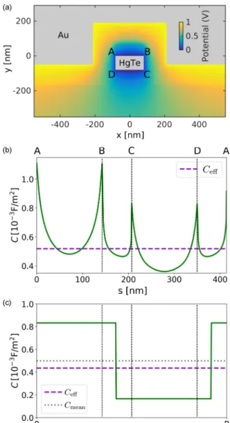
The PDE solver numerically yields solutions of the Laplace equation ∇2u(x,y)=0 for the heterostructure; an example with Vg =1V is given in Fig. 8(a). The induced surface charge density n(s) is then given by the gradient of the electric potential at the nanowire surface according to [31]
n(s)=(r0/e)(∇u)·eˆn, (7) where ˆen is the unit vector defining the surface normal, r is the dielectric constant of the insulating layer sur-
FIG. 8. Electrostatics of gated nanowires. (a) Electric potential u(x,y) across the heterostructure of device w2. (b) Capacitance profile C(s) along the circumference of nanowire w2 obtained via Eq. (7) from the electric potential depicted in (a). (c) Capacitance profile for the simplified model (see text) for parametersP =460 nm and Cmean=5×10⁻⁴Fm−2.
rounding the nanowire (r =3.5 for SiO2 and r =13.0 for HgCdTe), and 0 is the vacuum permittivity. The gate capacitance per unit charge, C(s)/e, defined as the surface electron density n(s) per gate voltage Vg, is then exported from the PDE solver. The surface charge density at arbitrary gate voltages is obtained by exploiting the linearity n(s)= [C(s)/e]Vg without the need for repeating the electrostatic simulation.
Figure8(b)shows the capacitanceC(s) resulting from the simulation. The large spikes in the capacitance stem from the sharp edges of the HgTe nanowire. Electrostatic simulations for a trapezoidal wire cross section with smoother gate profiles (not shown) show that our simple model overestimates the effective capacitance by <4%. Assuming metallic surface states and ignoring thus the quantum capacitance also leads
to capacitance values which are 5% larger. The finite length of our wires which is ignored in our 2D electrostatic model underestimates the capacitance by the fringe fields at the ends.
By analogy with finite length cylindrical capacitors the error for our wires is estimated to be10% [32]. As the errors due to the idealizations within our model tend to compensate each other, we expect the calculated values to be quite accurate.
V. BAND STRUCTURE OF GATED NANOWIRE A. Dirac surface Hamiltonian
Assuming that the bulk is insulating we model the HgTe nanowire by means of the Dirac surface Hamiltonian
H =vF[pzσz+(ps+eAs)σy], (8) whereAsis the vector potential which creates the longitudinal magnetic field. The numerical results presented in the follow- ing were obtained using the python software packageKWANT
[33]. Since KWANT utilizes tight-binding models, Eq. (8) needs to be discretized leading to fermion doubling [34,35].
In order to circumvent this, we add a small term quadratic in the momentum to the Hamiltonian which removes the artificial valleys from the considered energy range (for a recent discussion see Ref. [36]).
The magnetic flux and the curvature-induced Berry phase are implemented via the boundary condition
(z,s+P)=(z,s)ei2π(φ/φ0+1/2). (9) We further account for the effect of the top gate by adding the onsite energy [see corresponding Eq. (4) withgs =1]
Egate(s)= −hv¯ F
4π VgC(s)/e , (10) which induces the correct charge density n(s) along the nanowire circumference.
B. Gate effect: Simplified capacitance model
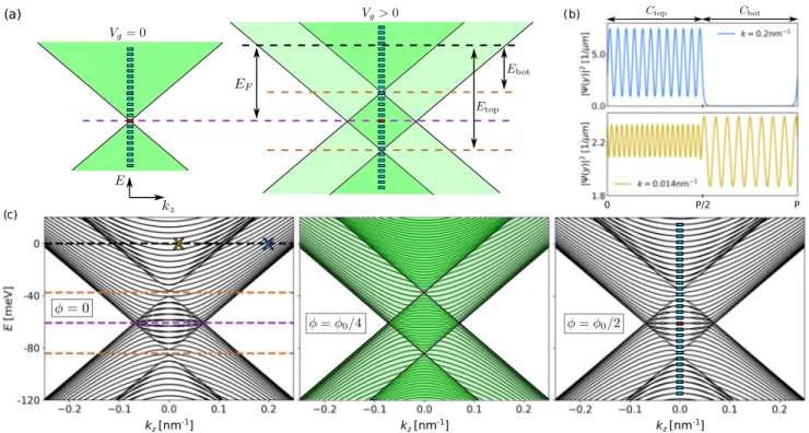
In order to illustrate the effect of the gate-induced potential on the band structure of a nanowire, we start with a simple step- shaped capacitance [see Fig.8(c)] before examining the more realistic case shown in Fig.8(b). In this simplified model,C(s) is determined by two capacitance values, one for the top surface Ctopand one for the bottom surfaceCbot, neglecting separate profiles at the narrow side surfaces. We chooseCtop/Cbot=5 for didactic purposes; in the experiments the ratio is≈2.
In the following, we first use a sketch of the resulting band structure in Fig.9(a)to explain the mechanisms that lead to the corresponding numerical results shown in Fig.9(c). For Vg=0 the band structure is given by a simple 1D Dirac cone [left panel in Fig.9(a)] with quantized subbands owing to the finite circumference. The positions of the subband minima at kz=0 are marked by blue rectangular boxes. The flux through the nanowire is chosen to be 0.5φ0 implying a state at zero energy (marked by a red box). ForVg >0 the Dirac cone splits, so that the distances between the common Fermi level EF and the two Dirac points areEtop =hv¯ F
4π ntopandEbot =
¯ hvF
√4π nbot [right panel in Fig.9(a)]. The difference arises since the top surface is filled faster than the bottom one. The Fermi energy is given by the averageEF =(Etop+Ebot)/2=
¯ hvF
π Vg/e(
Ctop+√ Cbot).
FIG. 9. Gate-dependent splitting of Dirac-type nanowire band structure for simplified step capacitance model for top and bottom surface [see Fig.8(c)]. (a) Sketch of the band structure for zero (left) and finite (right) gate voltage. Subband bottoms atkz=0 are indicated by blue rectangular boxes. (b) Probability distributions of two representative states along wire circumference with capacitancesCtopandCbotat top and bottom surface. The state in the upper (lower) panel corresponds to an energy marked by a blue (yellow) cross in panel (c). (c) Calculated band structures for three magnetic fluxesφ/φ0=0,1/4,1/2 forVg=1V andvF=5×10⁵m/s. In the left panel the dashed black horizontal line marks the Fermi level and the dashed yellow lines positions of shifted Dirac points. In the middle panel areas corresponding to flux-sensitive (insensitive) energy levels are marked by dark (light) green color.
Interestingly, the splitting of the Dirac cone does not influ- ence thekz=0 subband spacing, which is perfectly preserved.
Furthermore, for kz =0 the states can be divided into two groups. States with energies in the dark green regions in Fig.9 extend over the entire wire circumference and consequently are flux sensitive, whereas states with energies in the light green regions are localized on the upper or lower surface and hence are not susceptible to flux changes. Representative examples of both kinds of states are shown in Fig. 9(b). The reason for this peculiar behavior is Klein tunneling [37]. Modes at kz=0 perpendicularly hit the potential step associated with the capacitance profile of Fig.8(c)and are thus unaffected by its presence—Klein tunneling is perfect. On the other hand, for kz =0 the light green regions host states from one Dirac cone only, the dark green ones from both. Sincekz is conserved during tunneling, it is only in the dark green regions that electrons can Klein tunnel from one cone to the other, yielding hybridized extended states.
The different flux sensitivity of the two classes of states is also reflected in the numerical band structures shown in Fig.9(c)for three different fluxes: While the hyperbolic energy levels in the regimes corresponding to the light green areas are identical (on scales resolved in the figures) for all three fluxes, the energy levels belonging to the dark green areas obviously change with varying flux. We note in passing that trivial surface states which might form at the etched side surfaces do not contribute to the oscillations and thus to our analysis as they are localized at the sides.
C. Gate effect: Realistic capacitance model
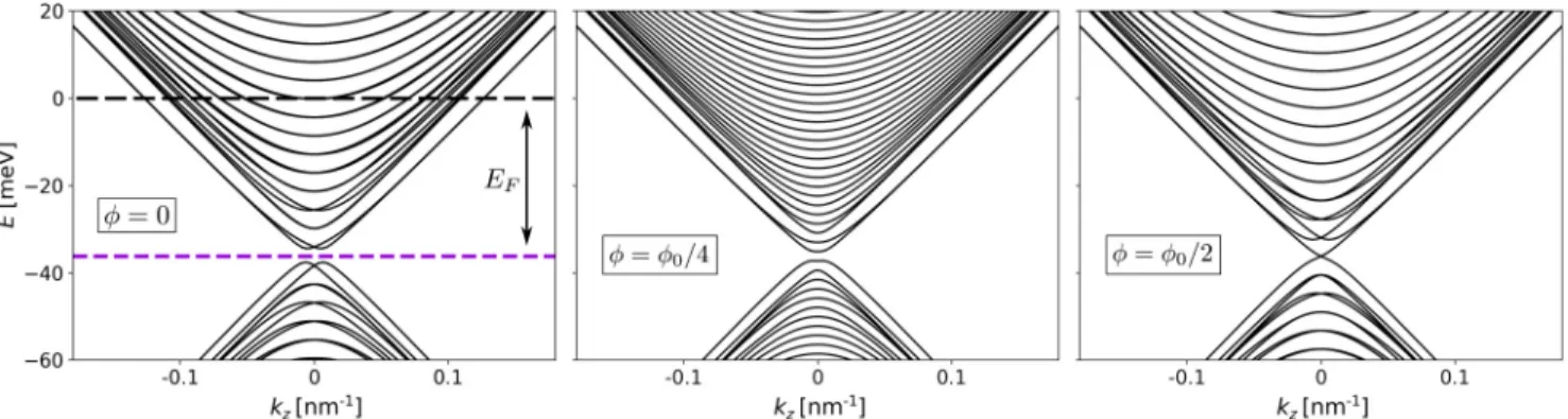
We now use these insights to examine the results obtained with the more realistic capacitance profile shown in Fig.8(b).
We present results for the nanowire geometry of sample w2; the other geometries do not qualitatively change the results. The corresponding band structures are presented in Fig.10for three different magnetic fluxes andVg =0.3 V. The interpretation of the band structure is not as simple as in the step capacitance model, as there are now four nanowire surfaces involved, each with a more complicated capacitance profile. Furthermore, the difference between the “potential bottoms” on each surface is smaller. However, the main features discussed in Sec.V B are still present, since they are actually independent of the capacitance profile shape.
Notably, Fig.10shows that thekz=0 subband spacing is perfectly preserved, even though the transversal wave vector kl(s)=√
4π n(s) is nowsdependent. Indeed, we can general- ize the discussion of the simplified step capacitance model: For kz=0 the motion is purely angular, and thus Klein tunneling is perfect irrespective of the complexities of the potential profile.
Hence, the electron wave function experiences an average of the gate potential, whose corresponding wave vector average fulfils
kl(s) ≡ 1 P
P
0
ds kl(s)=2π
P (l+0.5−φ/φ0). (11) This leads to a gate-independent subband spacingkl=2π/P that can be also derived by solving the Dirac equation forkz=
FIG. 10. Calculated band structures of device w2 based on the realistic capacitance model [see Fig.8(b)] forVg=0.3 V and three fluxes φ/φ0=0,1/4,1/2 (from left to right). The spacing between subband minima atkz=0 is constant for given flux.
0. Moreover, in the experimentally relevant parameter range, the Fermi level stays always above both Dirac points forVg >
0, and the subband minima atEFare always atkz=0.
For a general capacitance profileC(s) the Fermi energy is given by the average
EF =hv¯ F
4π Vg/e
C(s) =hv¯ F
4π VgCeff/e, (12) where the effective value Ceff≡ √
C(s)2 enters instead of the meanCmean≡ C(s)with. . .denoting the mean value along the circumference. The value forCeff calculated from the capacitance profile of w1 was used in the analysis of the experimental data in Fig.6. Note that the difference between Ceff andCmean is given by the variance of the capacitance profile Var(√
C(s))=Cmean−Ceff. For the step capacitance model with Ctop =5Cbot this difference is clearly visible [Ceff/Cmean≈0.87, see Fig.8(c)] but in the experiments it is typically quite small (e.g., for w2Ceff/Cmean≈0.985). As will become evident in the following, the perfect subband quantization and the fact that the subband minima are located atkz=0 are crucial ingredients to probe the signature of the Dirac surface states in transport.
VI. CONDUCTANCE SIMULATIONS
The conductance simulations presented in the following were carried out by using an extended version of the tight- binding model introduced in Sec.V A. The extended system includes coupling of the nanowire to leads with the same geometry as the nanowire but with negative onsite energy (i.e., highly-doped leads) to account for the wide leads in the experiment. Residual disorder in the wires used in experiment is modeled by adding a random disorder potentialV(r) defined through the correlator
V(r)V(r) =K0( ¯hvF)2
2π ξ2 e−|r−r|2/2ξ2. (13) Here,ξis the correlation length andK0determines the disorder strength [38].
Figure 11 shows the conductance G(Vg) for φ=0 and φ=0.5φ0. Both curves exhibit distinct oscillations on top of an increasing conductance background (similar to corresponding calculations in Ref. [7]). The anticorrelated behavior of the two oscillatory curves is due to the flux sensitivity of the states
near kz=0. The oscillatory behavior can be explained by the band structure: Whenever the Fermi energy approaches the bottom of one of the disorder-broadened subbands, the high density of states (associated with a van-Hove singularity) causes enhanced scattering and thus leads to a reduction of the conductance. By further increasing the gate voltage, the additional conductance channel fully opens and the Fermi energy leaves the vicinity of the van-Hove singularity, both effects leading to an increasing conductance. Thus, the con- ductance oscillation, related to successive subband opening, is a fingerprint of the band structure atkz=0, as also observed in the transport measurements. Due to the undisturbed subband quantization atkz=0, the distance between two conductance minima (one oscillation period) corresponds to a change of kl=2π/P in the Fermi wave vector, as in the case without any inhomogeneity caused by the top gate. However, the inhomogeneity enters via Ceff, which determines the Fermi wave vectorkF =
4π VgCeff/e[see Eq. (12)]. This justifies
FIG. 11. Calculated disorder-averaged conductance as a function of gate voltage (starting from the Dirac point) for zero flux (blue curve) and half a flux quantum (red curve). Calculations are performed for the nanowire geometry and usingCeffof sample w2. The average is taken over 103disorder configurations, based on the impurity model [Eq. (13)] with disorder strengthK0=0.2 and correlation lengthξ= P /100. Minima-maxima pairs in the conductance are marked with gray vertical lines. The inset shows the gate position of the minima- maxima pairs as a function of subband indexN, following the same evaluation as performed in Fig.5(b)for the experimental data.
a posteriorithe validity of Eq. (6) and the procedure used in Sec.III Bto analyze the experimental data if the surface states are Dirac-like.
Trivial surface states, however, are expected to have a quadratic dispersion, i.e., Klein tunneling is absent. Thus, the question arises whether theG(Vg) oscillations would still allow for the quantitative analysis performed in Sec.III B. Our simulations (not shown) for a quadratic dispersion reveal that for realistic gate-induced potentials the subband minima are still atkz=0 but now states belowEFcan be confined and thus become flux insensitive. Moreover, the subband quantization kl=2π/P is no longer preserved. However, for EF in our experimental range thekz=0 modes, which lead to the conductance oscillations, have an angular motion energy that is much larger than the gate potential. These states are thus flux sensitive and the subband quantization is only mildly affected (the degeneracy with respect to angular momentum is lifted). The lifting of the degeneracy is small compared to the subband spacing and cannot be observed within the experimental precision. For trivial surface states, we therefore indeed expect to measure a conductance with a similar shape as for Dirac states but with minima-maxima pairs following the spin-degenerate version (gs =2) of Eq. (6).
The inset of Fig. 11 shows a similar evaluation of the minima-maxima pairs as was done for the experimental data in Fig.5(b). The green parabolic curve describing spin-helical Dirac states according to Eq. (6) (with gs=1) matches perfectly with the results (black bullets) from the analysis of the gate-dependent conductance extrema, whereas the purple curve which holds for spin-degenerate trivial surface states (gs=2) is way off. Since we used Eq. (10) (with gs=1) to simulate the gate effect, the agreement was essentially expected. However, this analysis shows that if the surface states in 3D HgTe nanowires are Dirac-like, one should be able to obtain this signature of spin nondegenerate states by conductance measurements, despite the complicated po- tential profile induced by the top gate, as long as Ceff is known.
VII. CONCLUSIONS AND OUTLOOK
We fabricated nanowires based on strained HgTe and investigated in detail their peculiar transport properties in a joint experimental and theoretical effort. With regard to topo- logical insulator properties, HgTe-based systems represent an interesting alternative to Bi-based systems, as surface states in the former appear to be well decoupled from bulk states and ad- ditionally feature high surface mobilities [23]. The nanowires were built out of strained bulk systems in a well controlled way. In particular, we demonstrated that in these mesoscale conductors the topological properties of the corresponding bulk systems prevail and appear in combination with quantum coherent effects: The observedh/e-periodic Aharonov-Bohm- type conductance modulations due to a coaxial flux clearly indicate that transport along the wires is indeed both surface- mediated and quasiballistic, and additionally phase-coherent at micron scales. At low temperatures we moreover found that the extracted phase-coherence lengths are increased up to 5μm upon tuning the wire Fermi energy into the bulk band gap, where topological surface transport is singled out.
Besides the Aharonov-Bohm oscillations, we observed and examined in detail further distinct conductance oscillations appearing as a function of a gate voltage. We showed that the spacing of the observed regular gate-dependent oscilla- tions reveals the topological nature of the surface states: The gate dependence is only compatible with a model assuming nondegenerate (Dirac-type helical) surface states and rules out usual spin-degenerate states. This identification required on the theory side a quantitative electrostatic calculation of the gate-induced inhomogenous charge carrier density and associated capacitance of the whole (wire plus gate) system.
The latter entered the evaluation of the transport data and was furthermore integrated into numerical tight-binding magneto- transport calculations to show that the gate-dependent con- ductance oscillations obtained indeed agree with experiment.
This theoretical analysis also shed light on the role of Klein tunneling for the flux-sensitive surface states extending around the entire wire circumference, which govern the wire band structure.
Our finding that spin nondegenerate states exist on the wire surface suggests in particular that forφ/φ0=0.5, where time reversal symmetry is restored, the total number of left- or right-moving states is always odd at arbitrary Fermi level, implying a topologically protected perfectly transmitted mode.
In the presence of ans-wave superconductor, which opens a gap in the nanowire band structure via the proximity effect, Majorana fermions are expected to appear at the endings of the 3DTI wire, if the latter hosts such an odd number of states atEF [39,40]. This opens up the interesting possibility of switching from a topologically trivial (even number of states atEF) to a nontrivial situation (odd number of states at EF) by adding half a flux quantum through the wire’s cross section. This notably led to a recent proposal to use proximitized TI nanowires as building blocks for (coupled) topological Majorana qubits and networks of those [41].
While such proposals usually assume a uniform carrier density around the wire circumference, in experiments such density is expected to be strongly inhomogeneous, especially if the Fermi level is tuned via a top/back gate voltage. This raises the question of how substantially the topological behavior would be affected by strong inhomogeneities. Here we demonstrated through the quantitative analysis of our data that the essential characteristics of topological transport are indeed preserved under realistic experimental conditions. To conclude, our work puts forward HgTe-based topological insulator nanowires as a promising and realistic platform for exploring a wealth of phenomena based on spin-momentum locked quantum transport and topological superconductivity.
ACKNOWLEDGMENTS
This work was supported by Deutsche Forschungsge- meinschaft (within Priority Program SPP 1666 “Topological Insulators”) and the Elitenetzwerk Bayern Doktorandenkol- leg “Topological Insulators.” Support by Russian Federation President Grant No. MK-3603.2017.2 and RFBR Grant No.
17-42-543336 is also acknowledged. We thank J. Bardarson, J.
Dufouleur, S. Essert, and E. Xypakis for useful conversations.
[1] N. Z. Hasan and C. K. Kane,Colloquium: Topological insulators, Rev. Mod. Phys.82,3045(2010).
[2] J. H. Bardarson and J. E. Moore, Quantum interference and Aharonov-Bohm oscillations in topological insulators, Rep.
Prog. Phys.76,056501(2013).
[3] V. E. Sacksteder IV, K. B. Arnardottir, S. Kettemann, and I. A.
Shelykh, Topological effects on the magnetoconductivity in topological insulators,Phys. Rev. B90,235148(2014).
[4] H. Peng, K. Lai, D. Kong, S. Meister, Y. Chen, X.-L. Qi, S.-C.
Zhang, Z.-X. Shen, and Y. Cui, Aharonov-Bohm interference in topological insulator nanoribbons,Nat. Mater.9,225(2010).
[5] F. Xiu, L. He, Y. Wang, L. Cheng, L.-T. Chang, M. Lang, G.
Huang, X. Kou, Y. Zhou, X. Jiang, Z. Chen, J. Zou, A. Shailos, and K. L. Wang, Manipulating surface states in topological insulator nanoribbons,Nat. Nano6,216(2011).
[6] P. M. Ostrovsky, I. V. Gornyi, and A. D. Mirlin, Interaction- Induced Criticality inZ2Topological Insulators,Phys. Rev. Lett.
105,036803(2010).
[7] J. H. Bardarson, P. W. Brouwer, and J. E. Moore, Aharonov-Bohm Oscillations in Disordered Topological Insu- lator Nanowires,Phys. Rev. Lett.105,156803(2010).
[8] Y. Zhang and A. Vishwanath, Anomalous Aharonov-Bohm Conductance Oscillations from Topological Insulator Surface States,Phys. Rev. Lett.105,206601(2010).
[9] G. Rosenberg, H.-M. Guo, and M. Franz, Wormhole effect in a strong topological insulator,Phys. Rev. B82,041104(2010).
[10] T. Ando and H. Suzuura, Presence of perfectly conducting channel in metallic carbon nanotubes,J. Phys. Soc. Jpn. 71, 2753(2002).
[11] M. Tian, W. Ning, Z. Qu, H. Du, J. Wang, and Y. Zhang, Dual evidence of surface Dirac states in thin cylindrical topological insulator Bi2Te3nanowires,Sci. Rep.3,1212(2013).
[12] J. Dufouleur, L. Veyrat, A. Teichgräber, S. Neuhaus, C. Nowka, S. Hampel, J. Cayssol, J. Schumann, B. Eichler, O. G. Schmidt, B. Büchner, and R. Giraud, Quasiballistic Transport of Dirac Fermions in a Bi2Se3 Nanowire,Phys. Rev. Lett.110,186806 (2013).
[13] M. Safdar, Q. Wang, M. Mirza, Z. Wang, K. Xu, and J. He, Topological surface transport properties of single-crystalline snte nanowire,Nano Lett.13,5344(2013).
[14] S. S. Hong, Y. Zhang, J. J. Cha, X.-L. Qi, and Y. Cui, One- dimensional helical transport in topological insulator nanowire interferometers,Nano Lett.14,2815(2014).
[15] S. Cho, B. Dellabetta, R. Zhong, J. Schneeloch, T. Liu, G.
Gu, M. J. Gilbert, and N. Mason, Aharonov-Bohm oscilla- tions in a quasi-ballistic three-dimensional topological insulator nanowire,Nat. Commun.6,7634(2015).
[16] L. A. Jauregui, M. T. Pettes, L. P. Rokhinson, L. Shi, and Y. P.
Chen, Magnetic field-induced helical mode and topological tran- sitions in a topological insulator nanoribbon,Nat. Nanotechnol.
11,345(2016).
[17] J. Kim, A. Hwang, S.-H. Lee, S.-H. Jhi, S. Lee, Y. C. Park, S. Kim, H.-S. Kim, Y.-J. Doh, J. Kim, and B. Kim, Quantum electronic transport of topological surface states inβ-Ag2Se nanowire,ACS Nano10,3936(2016).
[18] C. Brüne, C. X. Liu, E. G. Novik, E. M. Hankiewicz, H.
Buhmann, Y. L. Chen, X. L. Qi, Z. X. Shen, S. C. Zhang, and L. W. Molenkamp, Quantum Hall Effect from the Topological Surface States of Strained Bulk HgTe,Phys. Rev. Lett. 106, 126803(2011).
[19] O. Crauste, Y. Ohtsubo, P. Ballet, P. A. L. Delplace, D. Carpen- tier, C. Bouvier, T. Meunier, A. Taleb-Ibrahimi, and L. Lévy, Topological surface states of strained Mercury-Telluride probed by ARPES,arXiv:1307.2008.
[20] S.-C. Wu, B. Yan, and C. Felser,Ab initiostudy of topological surface states of strained HgTe, Europhys. Lett. 107, 57006 (2014).
[21] P. G. Silvestrov, P. W. Brouwer, and E. G. Mishchenko, Spin and charge structure of the surface states in topological insulators, Phys. Rev. B86,075302(2012).
[22] K.-M. Dantscher, D. A. Kozlov, P. Olbrich, C. Zoth, P. Fal- termeier, M. Lindner, G. V. Budkin, S. A. Tarasenko, V. V.
Bel’kov, Z. D. Kvon, N. N. Mikhailov, S. A. Dvoretsky, D.
Weiss, B. Jenichen, and S. D. Ganichev, Cyclotron-resonance- assisted photocurrents in surface states of a three-dimensional topological insulator based on a strained high-mobility HgTe film,Phys. Rev. B92,165314(2015).
[23] D. A. Kozlov, Z. D. Kvon, E. B. Olshanetsky, N. N. Mikhailov, S. A. Dvoretsky, and D. Weiss, Transport Properties of a 3D Topological Insulator based on a Strained High-Mobility HgTe Film,Phys. Rev. Lett.112,196801(2014).
[24] A. G. Aronov and Yu. V. Sharvin, Magnetic flux effects in disordered conductors,Rev. Mod. Phys.59,755(1987).
[25] S. Washburn and R. A. Webb, Aharonov-Bohm effect in normal metal quantum coherence and transport, Adv. Phys.35, 375 (1986).
[26] D. A. Kozlov, D. Bauer, J. Ziegler, R. Fischer, M. L. Savchenko, Z. D. Kvon, N. N. Mikhailov, S. A. Dvoretsky, and D. Weiss, Probing Quantum Capacitance in a 3D Topological Insulator, Phys. Rev. Lett.116,166802(2016).
[27] A. Savitzky and M. J. E. Golay, Smoothing and differentiation of data by simplified least squares procedures,Anal. Chem.36, 1627(1964).
[28] Ö. Gül, N. Demarina, C. Blömers, T. Rieger, H. Lüth, M. I.
Lepsa, D. Grützmacher, and Th. Schäpers, Flux periodic magne- toconductance oscillations in GaAs/InAs core/shell nanowires, Phys. Rev. B89,045417(2014).
[29] A. Logg, K.-A. Mardal, G. N. Wellset al.,Automated Solution of Differential Equations by the Finite Element Method(Springer- Verlag, Berlin, Heidelberg, 2012).
[30] C. Geuzaine and J.-F. Remacle, Gmsh: A three-dimensional finite element mesh generator with built-in pre- and post- processing facilities,International Journal for Numerical Meth- ods in Engineering79,1309(2009).
[31] M.-H. Liu, Theory of carrier density in multigated doped graphene sheets with quantum correction, Phys. Rev. B 87, 125427(2013).
[32] B. N. Das and S. B. Chakrabarty, Capacitance and charge distribution of two cylindrical conductors of finite length,IEE Proceedings - Science, Measurement and Technology144,280 (1997).
[33] C. W. Groth, M. Wimmer, A. R. Akhmerov, and X. Waintal, Kwant: A software package for quantum transport,New J. Phys.
16,063065(2014).
[34] L. Susskind, Lattice fermions,Phys. Rev. D16,3031(1977).
[35] R. Stacey, Eliminating lattice fermion doubling,Phys. Rev. D 26,468(1982).
[36] K. M. M. Habib, R. N. Sajjad, and A. W. Ghosh, Modified Dirac Hamiltonian for efficient quantum mechanical simulations of micron sized devices,Appl. Phys. Lett.108,113105(2016).
[37] P. E. Allain and J. N. Fuchs, Klein tunneling in graphene:
Optics with massless electrons, Eur. Phys. J. B 83, 301 (2011).
[38] For a detailed discussion of scattering in quasiballistic Dirac nanowires, see Ref. [42].
[39] A. Cook and M. Franz, Majorana fermions in a topological-insulator nanowire proximity-coupled to an s-wave superconductor, Phys. Rev. B 84, 201105 (2011).
[40] F. de Juan, R. Ilan, and J. H. Bardarson, Robust Transport Signatures of Topological Superconductivity in Topological Insulator Nanowires,Phys. Rev. Lett.113,107003(2014).
[41] J. Manousakis, A. Altland, D. Bagrets, R. Egger, and Y. Ando, Majorana qubits in a topological insulator nanoribbon architec- ture,Phys. Rev. B95,165424(2017).
[42] J. Dufouleur, E. Xypakis, B. Büchner, R. Giraud, and J. H.
Bardarson, Suppression of scattering in quantum confined 2D- helical Dirac systems,arXiv:1709.00301.