Quantum Hall effect and Landau levels in the three-dimensional topological insulator HgTe
J. Ziegler,1D. A. Kozlov,2,3N. N. Mikhailov,3S. Dvoretsky ,3and D. Weiss 1
1Experimental and Applied Physics, University of Regensburg, D-93040 Regensburg, Germany
2A. V. Rzhanov Institute of Semiconductor Physics, Novosibirsk 630090, Russia
3Novosibirsk State University, Novosibirsk 630090, Russia
(Received 4 February 2020; accepted 11 June 2020; published 1 July 2020)
We review low- and high-field magnetotransport in 80-nm-thick strained HgTe, a material that belongs to the class of strong three-dimensional topological insulators. Utilizing a top gate, the Fermi level can be tuned from the valence band via the Dirac surface states into the conduction band and allows studying Landau quantization in situations where different species of charge carriers contribute to magnetotransport. Landau fan charts, mapping the conductivityσxx(Vg,B) in the whole magnetic field–gate voltage range, can be divided into six areas, depending on the state of the participating carrier species. Key findings are (i) the interplay of bulk holes (spin degenerate) and Dirac surface electrons (nondegenerate), coexisting forEF in the valence band, leads to a periodic switching between odd and even filling factors and thus odd and even quantized Hall voltage values.
(ii) We found a similar though less pronounced behavior for coexisting Dirac surface and conduction band electrons. (iii) In the bulk gap, quantized Dirac electrons on the top surface coexist at lowerBwith nonquantized ones on the bottom side, giving rise to quantum Hall plateau values depending—for a given filling factor—on the magnetic field strength. In strongerBfields, Landau level separation increases; charge transfer between different carrier species becomes energetically favorable and leads to the formation of a global (i.e., involving top and bottom surfaces) quantum Hall state. Simulations using the simplest possible theoretical approach are in line with the basic experimental findings, describing correctly the central features of the transitions from classical to quantum transport in the respective areas of our multicomponent charge carrier system.
DOI:10.1103/PhysRevResearch.2.033003
I. INTRODUCTION
The quantum Hall effect (QHE) [1] and Shubnikov–de Haas (SdH) oscillations with zero resistance states [2] are hall- marks of two-dimensional electron (2DES) or hole (2DHS) systems, realized, e.g., in semiconductor heterostructures [3]
or in graphene [4]. These phenomena are closely connected to the discrete Landau level (LL) spectrum of charge carriers in quantizing magnetic fields. These Landau levels are spaced by the cyclotron energy ¯hωc( ¯his the reduced Planck constant andωc the cyclotron frequency) and form, as a function of magnetic field and Landau level indexn, the Landau fan chart.
In conventional two-dimensional systems one type of charge carrier, i.e., electrons or holes, prevails, giving rise to one Lan- dau fan chart and a regular sequence of SdH peaks or quantum Hall plateaus, which occur in equidistant steps on an inverse magnetic field scale, 1/B.A more complicated situation arises when two-dimensional electron and hole systems coexist as in heterojunctions with a broken gap (type III heterojunction), e.g., in InAs/GaSb quantum wells [5]. This gives rise to hy- bridization [6] and a complicated interplay between LLs [7].
With the advent of three-dimensional (3D) topological insula-
Published by the American Physical Society under the terms of the Creative Commons Attribution 4.0 International license. Further distribution of this work must maintain attribution to the author(s) and the published article’s title, journal citation, and DOI.
tors (TIs) [8–11] a new class of two-dimensional electron sys- tems appeared on the scene where the two-dimensional charge carrier system consisting of Dirac fermions forms a closed surface “wrapped” around the insulating bulk. In contrast to a conventional two-dimensional electron gas, these Dirac surface states are non–spin degenerate and have their spin orientation locked to their momentum. The unusual topology of the two-dimensional Dirac system creates a manifold of possibilities of how the charge carriers on the top and bottom surfaces interact for different positions of Fermi level and magnetic field strength. For a Fermi-level position in the conduction band, e.g., three different charge carrier species with different densities and mobilities exist: bulk electrons, which are spin degenerate, and nondegenerate Dirac surface electrons on the top and bottom surfaces. Here, we ignore charge carriers on the side facets, parallel to the applied mag- netic field, which play only a minor role in the context of the present investigations. While SdH oscillations and the QHE have been observed in various TI materials [12–17], strained HgTe, a strong topological insulator [18], is insofar special, as it features unprecedented high mobilitiesμwithμB1 at magnetic fields as low as 0.1 T. This material thus serves as a model system to explore Landau quantization and mag- netotransport in a situation where different types of charge carriers exist together. However, the physics discussed below is also valid for other topological insulator materials in which different kinds of charge carriers coexist at the Fermi level.
The first observation of the QHE in strained films of HgTe was reported in Ref. [12], which also presents calculations of
the band dispersion of the surface states on the top and bottom surfaces. Correspondingab initiocalculations computing the band gap in which the TI surface states reside as a function of strain (i.e., lattice mismatch between HgTe and substrate) were presented in Ref. [19]. Typical band gaps for HgTe on CdTe are of the order of 20 meV. Since in the initial exper- iment the position of the Fermi levelEF was unknown, we explored the QHE effect and SdH oscillations systematically as a function of a top gate voltage [13]. The top gate enables tuning the Fermi level from the valence band, through the gap region with gapless surface states into the conduction band. As the QHE is also observed when the Fermi level is supposedly in the conduction band, Brüne et al.claimed that due to screening effects the Fermi level is pinned in the band gap so that only Dirac surface states exist at EF
[20]. However, the underlying “phenomenological effective potential for the sake of keeping the Fermi level within the bulk gap is not proper” [21]. Below we show not only that the Fermi level can be easily tuned from the valence band into the conduction band, but we provide a comprehensive picture of Landau quantization and quantum Hall effect in the multicarrier system of a topological insulator.
II. CHARACTERIZATION OF SAMPLES
The 80-nm-thick HgTe material, investigated here, has been grown by molecular beam epitaxy on (013)-oriented (GaAs); similar wafers have been used previously to study magnetotransport [13], cyclotron resonance [22], or quantum capacitance [23]. A π-phase shift of quantum capacitance oscillations [23], geometric resonances in antidot arrays [24], and the subband spectrum of HgTe nanowires made of this material [25] confirm the topological nature of the surface states. As shown in Fig. 1(a), the heterostructure includes a 20-nm-thick CdxHg1–xTe buffer layer on either side and a 40-nm-thick CdTe cap layer to protect the pristine HgTe surfaces. A top gate stack consisting of 30 nm of SiO2, 100 nm of Al2O3and Ti/Au enables control of the charge carrier density and thus of the Fermi level via gating. Thus, the Fermi energy EF can be tuned from the valence band (VB) into the bulk gap and further into the conduction band (CB) [13,21,23]. For magnetotransport measurement we use a stan- dard Hall bar geometry of length 1100μm and width 200μm, sketched in Fig. 1(b), and temperatures ofT =50 mK; the magnetic field B points perpendicular to the sample plane.
We use a low ac current of 10 nA flowing through the Hall bar to prevent heating of the carriers. To measure longitudinal and transversal resistivitiesρxxandρxy, respectively, we use standard low-frequency lock-in techniques.
Figure 1(c) shows low-field SdH oscillations taken at different gate voltages, i.e., Fermi level positions. AtVg = –1.5 V the Fermi level is in the valence band while for+1 V it is in the bulk gap; a simplified band structure is shown in Fig.2(a)for guidance. Figure1(d)displays the typicalVg
dependence of the resistivityρxx, measured atB=0, and of the Hall resistance ρxy, taken at 0.5 T. The traces are very similar to the ones we reported previously [13,23–26]. The ρxxtrace exhibits a maximum atVg= −0.15 V near the charge neutrality point (CNP, atVg=0.25 V), and two characteristic weak humps at 0.4 and 1.25 V. The latter are due to enhanced
FIG. 1. (a) Scheme of the heterostructure cross section. (b) Sketch of the 200-µm-wide and 1100-µm-long Hall bar. (c) Lon- gitudinal resistivityρxx(B) at differentVg forEF in the conduction band (2, 1.5 V), gap (1 V), and valence band (–0.5, −1.5 V).
(d)Vgdependence ofρxx(left axis, light blue) atB=0 andρxy(right axis, dark blue) atB=0.5 T. The vertical arrows show the charge neutrality point (CNP), top of the bulk valence (EV), and bottom of the conductance band (EC), respectively. Here,EV andECmark the gate voltage at which bulk hole and bulk electron densities vanish, respectively. (e) Electronns(Vg) and hole densities ps(Vg) extracted from the Hall slope, two-carrier Drude model, and SdH oscillations.
The analysis follows Ref. [13] and yields positions of the valence and conduction band edges atVg(EV)=0.45 V andVg(EC)=1.2 V, respectively, marked in (d). (f) Pictorial of the capacitively coupled layers in the 3D TI sample which form the basis of our electrostatic model. (g) Electronns(Vg) and hole densities ps(Vg) as calculated with our electrostatic model. The densities which can be directly compared with (e) are shown as solid lines, the ones which are not directly accessible as dashed lines.
scattering of surface electrons and bulk carriers at the band edges, i.e., valence band (VB, marked byEV on theVgaxis) and conduction band (CB, markedEC) [13]. Near the CNP the Hall resistance ρxy changes sign as the majority charge carrier type changes from electrons to holes whenEF enters the VB. Closer examination of magnetotransport data using the Drude model and the periodicity of SdH oscillations, as in Refs. [13,23], reveals partial densities and precise values of EV andEC. The result of such analysis is shown in Fig.1(e).
AboveEV, electron densitiesns are extracted from the slope of the Hall resistance (nsHall) and from the periodicity of the SdH oscillations. SdH oscillation periods reveal different carrier densities, depending on whether the data are taken at low (nSdH,lows ) or high magnetic fields (nSdH,highs ). WhilenHalls andnSdH,highs represent the total charge carrier density of the system (and therefore coincide),nSdH,lows represents the top surface electrons only [13,23]. The reason for the latter is
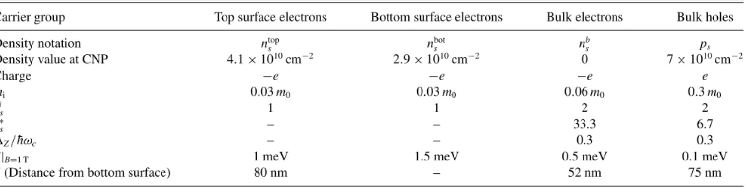
FIG. 2. (a) Schematic band structure of strained HgTe. Conduc- tion and valence band edges are marked byEC and EV, the Dirac point, which is located in the valence band, byEDF. The topological Dirac surface states are shown in blue. Note that the position of EF within the band structure is usually different for top and bottom surfaces. (b) The quantum Hall effect in strained 80-nm HgTe, shown for different gate voltagesVg, can stem from surface electrons in the gap (with additional contributions from bulk electrons in the CB) and bulk holes in the VB. This is reflected by the changing sign of the Hall slope when tuning the gate voltageVgacross the charge neutrality point.
that the SdH oscillations of the bottom side electrons are at these small magnetic fields not yet sufficiently resolved, in contrast to the ones on the top surface. We will address this topic further below. An example of low-field SdH oscillations, taken at different gate voltages, is shown in Fig. 1(c). The traces exhibit pronounced oscillations starting below 0.5 T, indicating the high quality of the HgTe layer. Below EV, surface electrons and bulk holes coexist [see, e.g., Fig.2(a)]
and the corresponding densities can be extracted using a two- carrier Drude model [13]. ExtrapolatingpDrudes (Vg) in Fig.1(e) toVg=0 yields the exactVg position of EV, and coincides with theρxxhump, mentioned above. The change in slope of the top surface carrier densitynSdHs ,low atVg=0 signals that EF crosses the conduction band edge [13,23].
Figure 1(f) illustrates the different charge carrier species and the basic geometry of our electrostatic model, briefly discussed below, which is used to relate the different carrier densities to the applied gate voltage. The result of our calcula- tions is shown in Fig.1(g). Using the parameters of TableIthe model reproduces the experimental data quite well as can be clearly seen by comparison with the experiment in Fig.1(e).
Figure2(b)demonstrates that the system displays a well- developed quantum Hall effect. For negative gate voltagesVg, the quantized plateaus stem from bulk holes. For positiveVg, the slope ofρxychanges sign and the plateaus stem from Dirac surface states with contributions from conduction band states at higher positive Vg. At positive or negative bias voltages the band bending is expected to confine the bulk states at the surface so that they form a conventional two-dimensional electron or hole gas. Thus, the notion of bulk electrons or bulk holes refers to states which are, when biased, largely confined at the surface as is sketched in Fig.4(a).
III. EXPERIMENTAL DATA OVERVIEW
To get further insight into the interplay of the different carrier species in the system we take a closer look at the formation of Dirac state LLs and their interaction with bulk carriers’ LLs. To this end, we measured the magnetotransport coefficients ρxx and ρxy at a temperature of 50 mK and magnetic fields up to 12 T. The measured resistivity values were converted into conductivities by tensor inversion. The corresponding data set is plotted in Fig. 3(a) as a normal- ized conductivity σxx(Vg,B) where each horizontal cut was normalized to itsB-field average. Lines of high conductivity are colored from yellow to light blue and represent Landau levels, while deep blue color corresponds to the gaps between LLs. The investigated Vg range spans Fermi level values from inside the valence band to deep into the conduction band. In strong magnetic fields, the data show bothn- and p-type Landau fans, almost symmetrical with respect to the CNP, at which surface and bulk electrons counterbalance bulk holes. The well-resolved ν=0 state is either a magnetic field induced insulator state at the CNP or can be viewed as formation of counterpropagating edge states [27–29]. The nature of this state is out of the scope of the present work.
To increase resolution and visibility in the low-field region, we present in Fig.3(b)the second derivative∂2σxx/∂Vg2of the above data for smaller rangesB<5 T andVg= −2 to 2 V.
Here, yellow regions of negative curvature of ∂2σxx/∂Vg2
correspond to maxima in the conductivity, i.e., the position of LLs. Green and blue areas in between represent gaps. The respective data uncover a complex oscillation pattern with splitting, kinks, and crossings of LLs. These features occur in different sections of the (Vg,B) parameter space, indicating that several groups of carriers are involved in the formation of
TABLE I. Parameters of the different groups of carriers used in the model.
Carrier group Top surface electrons Bottom surface electrons Bulk electrons Bulk holes
Density notation ntops nbots nbs ps
Density value at CNP 4.1×1010cm−2 2.9×1010cm−2 0 7×1010cm−2
Charge −e −e −e e
mi 0.03m0 0.03m0 0.06m0 0.3m0
gis 1 1 2 2
g∗s – – 33.3 6.7
Z/hω¯ c – – 0.3 0.3
Г|B=1 T 1 meV 1.5 meV 0.5 meV 0.1 meV
d(Distance from bottom surface) 80 nm – 52 nm 75 nm
FIG. 3. (a) Color map of the normalized longitudinal conductivityσxx(Vg,B) for magnetic fields up toB=12 T. Conductance maxima are yellow and green; filling factors for the bluish energy gaps are shown in white. Data are normalized to the average value for a givenBvalue.
We use a logarithmic color scale to enhance the visibility of features throughout the entire investigated parameter space. (b) Excerpt of the data in (a), shown as the second derivative∂2σxx/∂Vg2. Yellow lines correspond, as above, to Landau levels, and green and blue regions to Landau gaps. White dashed lines separate the investigated parameter space (Vg,B) into distinct sections discussed in the text. (c) Simulated density of states based on the simple model described in the Appendix. Maxima (minima) of the DoS are shown in yellow (blue) and correspond to maxima (minima) ofσxx(Vg,B), i.e., to LL positions (gaps).EV,EC, CNP, andEDF,toplabel points on the gate voltage axis, which were matched to the experimentally obtained values. White lines represent the fan chart originating from the CNP.
LLs. The analysis of the data can be done in several ways.
One option is to exactly calculate LL positions using the k·pmethod and trying to fit the whole set of data. However, such an approach entails significant computational difficulties because Schrödinger and Poisson equations need to be calcu- lated self-consistently for every point in the (Vg,B) parameter space. Still, this procedure would not promote true insight into the underlying physics. Instead, we introduce a minimal but adequate computational model, which semiquantitatively agrees with the experimental data. The model is based on our capacitance model [23] but extended to the case of nonzero magnetic fields. While its detailed description is presented in the Appendix, we address here only the crucial points:
Within the model, each group of carriers is characterized by its own set of LLs, typified by the charge they carry (empty LLs bear no charge, while occupied ones are negatively or positively charged), Landau degeneracy (spin degenerate or not), LL dispersion, and LL broadening. Further, a joint Fermi levelEF and the total charge carrier density (ns−ps), which depends linearly onVg, characterize the entire system. The total charge is distributed among all LLs, determined by the position of the Fermi level. Here, we need to take into account the electrostatics of the system: Changes of the electric fields in the device due to changes of the carrier densities within the subsystem via the gate shifts the band edges and thus the corresponding origins of the LLs. The effect of electrostatics on the position of LLs for several gate voltages is shown in Fig.4, described in more detail in the caption and in Fig. S1
in the Supplemental Material [30]. It is important to note that the band edges and thus the origin of the LL fan charts depend on the gate voltageVg. In the limit of zero magnetic field, the model gives identical results (i.e., bands bending and partial densities) as the capacitance model [23]. The output of the calculation is the position of the Fermi level, both partialνi and total filling factorsν, partial densities of states (DOS)Di, and Hall conductivitiesσxyi for specifiedBandVg
values. Figure3(c) shows an example of such a calculation which displays the total density of states as a function ofVg
andB, thus reconstructing the LLs within the (Vg,B) map.
Above 4 T on the hole side and above 6–8 T on the electron side the calculated LLs form simple fan charts which both emanate from the CNP. This is in excellent agreement with the experiment in Fig.3(a).
The combined analysis of experimental data and simu- lations allows us to classify six distinct regions within the σxx(Vg,B) map, shown in Fig. 3(b). We will discuss the regions marked from 1 to 6 below with the help of our model calculations. Region 1 covers the high-magnetic-field region where the system is fully quantized, so that all LLs are resolved. Here, the total densityns−psdetermines the filling factors and the Landau level positions. By extrapolating the LLs in Fig.3(a)from high fields down toB=0 (not shown) all the lines meet at the CNP. Conversely, region 6 located at fields below 0.4 T describes fully classical and diffusive transport. At intermediate magnetic fields, i.e., in large parts of regions 2–5, only some of the LLs, e.g., on the top surface,
E
FE
cEv
DFbott
E
cE
vE
cE
vE
cE
vDFtop DFbott DFtop DFbott DFtop DFbott
E
F(a)
0 1 2 3 4
-20 -15 -10 -5 0 5 10 15 20
0 1 2 3 4 0 1 2 3 4-20
-15 -10 -5 0 5 10 15 20
0 1 2 3 4
Ev Ec
EDF, top EDF, bot
Vg = -1.5 V (Valence band) (b)
Vg = 0.25 V (CNP)
B (T)
)Vem( E
Vg = 1.5 V (Cond band)
Vg = 0.9 V (Gap) DFtop
FIG. 4. When a gate voltage is applied, the charge carriers of the system rearrange. While the exact solution requires a complicated self-consistent solution of Schrödinger and Poisson equations, most of the features observed in magnetotransport can be explained by a simple electrostatic model. Within this model, each group of carriers is modeled by a 2D system of electrons or holes of zero thickness. Each layer generates its own set of Landau levels emerging at different energies, but with common Fermi level position. Charged 2D surfaces cause, like a charged capacitor plate, 1D electric fields across the structure leading to electrostatic potentials, depending linearly on the charge. These potentials change with gate voltage, thus shifting the band edges, from which the Landau levels emanate. (a) Schematic band diagrams of the investigated HgTe 3D TI system at different gate voltagesVg(VB:Vg=–1.5 V; CNP:Vg=0.25 V; gap:Vg=0.9 V; CB:Vg=1.5 V).
Occupied hole states are shown in red, occupied states of surface electrons in dark blue, and bulk states in orange. The Dirac points of top and bottom surfaces in strained HgTe thin films are located belowEV, as shown in the diagrams. (b) Landau level spectra at different bias conditions used in the model. The corresponding band bending is shown above in (a). The model calculations include Zeeman splitting for spin-degenerate bulk states (orange for conduction band; red for valence band states). Landau fans that do not cross the Fermi energyEF (i.e., empty levels) are shown as dotted lines.
are resolved so that combinations of quantized and diffusive transport arise. In region 4, EF is in the gap so that only topological states on the top and bottom surfaces are present at the Fermi level, but no bulk states. In regions 2 and 3, bulk holes dominate the Landau spectrum but coexist with surface electrons on top and bottom. The coexisting surface electron and bulk hole Landau fans cause an intricate checkerboard pattern in region 3. In region 5, the surface states coexist with bulk electrons that are filled whenEF >EC. Below, we consider these regions in more detail.
IV. WEAK AND STRONG MAGNETIC FIELD LIMITS The behavior of the system in the limits of small and large magnetic fields is easily accessible. At small magnetic fields, i.e., in region 6 of Fig. 3(b), the LL separation is smaller than the LL broadening and transport is fully dif- fusive. In this regime the classical multicomponent Drude
model characterizes transport. The model assigns each group of carriers, labeled by indexi, its own set of densityns,i and mobilityμi. The resulting total conductivity is then the sum of the partial conductivities [13,31]. This model explains the observed effects, including the nonlinearρxy(B) trace as well as a distinct positive magnetoresistance when bulk holes and surface electrons coexist in the valence band [13]. The very low density of bulk carriers in the gap is reflected by the darker blue color (i.e., lowσxx) with a sharp transition at the conduction band edgeVg(EC) and a smoother one atVg(EV) in Fig.3(a). The color difference between gap and bulk bands regions reflects the effect of classical localization of charge carriers described by σxx,i∝ns,i/μiB2 in classically strong fields (μB1, here typically valid forB>0.1 T). Thus, the magnetoconductivityσxxis lowest in the gap where the bulk carrier concentration with low mobility is significantly lower than the one in conduction band. The contrast of the color at EC in Fig.3(a)directly confirms that the Fermi level can be
tuned into the conduction band, in contrast to earlier claims [20].
The opposite case of strong magnetic fields is characterized by completely (spin) resolved LLs and well-defined QHE state. On the electron side, e.g., three fan charts—one for the top surface, one for the bottom surface, and, for the Fermi level in the conduction band, one for bulk electrons—coexist.
For constant carrier density (gate voltage), the Fermi level jumps with increasing magnetic field from a fully occupied LL of the top surface electrons to the next lower one, belonging, e.g., to the electrons on the bottom surface. This process is connected with a transfer of charges from the top to the bottom surface. The SdH oscillations reflect, in this case, the total carrier density of bottom plus top surface electrons.
The total charge densityns−pscontrols the total filling factor νand the position of the Landau levels. On the electron side, this means that the total electron density (bulk plus surface density) determines the filling factor, while in the valence band (where surface electrons and bulk holes coexist) it is the difference of electron and hole densities. The Landau fan chart, constructed from high-field σxx data in Fig. 3(a), is symmetric with respect to the CNP and periodic inVg and 1/B. The entire high-field LLs in Fig. 3(a), extrapolated to zero magnetic field, have their origin at the CNP. The pattern is very similar to that observed in other electron-hole systems, e.g., in graphene [4,32], but without graphene’s spin and valley degeneracy. However, there is a quantitative asymmetry between electrons (positive filling factors) and holes (negative filling factors): The conductivity minima for electrons are deeper than for holes; at the same time, the conductivity maxima are broader for holes. This asymmetry reflects the difference of effective masses and cyclotron gaps, which differ by one order of magnitude [22,33] between the carrier types.
The transition between the low-field regime, at which the LL fans are determined by the respective electron or hole density, and the high-field regime, where the fans follow the total charge carrier densityns−ps, occurs when the LL separation is sufficiently large compared to the LL broadening.
V. COEXISTENCE OF QUANTIZED AND DIFFUSIVE CARRIERS IN THE BULK GAP
Here we focus on the bulk gap region, labeled as region 4 in Fig.3(b)and magnified in Fig.5(a). In this region, the Fermi level is in the bulk gap and only Dirac surface states contribute to transport. The SdH oscillations appear from 0.3 T on and show a uniform pattern, strictly periodic inVg and 1/B, until a magnetic field ofB=1.5–2 T is reached. This regular behavior reflects that only the motion of one carrier species, i.e., the electrons on the top surface, is quantized [13,23].
The electrons on the bottom surface have lower density and mobility and their LL spectrum is not yet resolved. The bottom electrons thus contribute a featureless background to the conductivity. Theσxy(Vg) data in Fig.5(c)clearly show this diffusive background: The individual low-fieldσxy(Vg) traces show pronounced nonquantized Hall plateaus with values, which increase with increasingBfield [see red dashed lines in Fig.5(c)]. This behavior can be reproduced by adding the Hall conductivities of the top and bottom surface electrons:
σxytot=σxyquant+σxydiff =νtope2/h +μnbots eμB/(1+(μB)2).
Here, σxyquant is the quantized Hall conductivity of the top surface, depending on the corresponding filling factorνtopand the carrier density of the back surface,nbots , which depends only weakly on the gate voltage. We estimate the increase of the plateau values with increasingB in the Supplemental Material [30], which is in good agreement with experiment.
The SdH oscillations occurring below 1.5 T are described by a single fan chart, shown as dark blue lines in Fig.5(a).
The fan chart emerges atVg=0.05 V, corresponding to a position of the Fermi level in the valence band. This point can be viewed as a virtual Dirac point, at which the density of the top surface Dirac seemingly becomes zero. However, this would only be the case if the filling rate of the top surface electrons was constant, which is not the case. WhenEF enters the valence band, the filling rate decreases precipitously and the fan chart no longer fits the observedσxymaxima [see dark blue dashed lines in Fig. 5(a)]. The actual gate voltage at whichntops =0 holds is located much deeper in the valence band and labeledEDF,top,shown in Fig.5(b). Typical partial densities of the different charge carriers and the corresponding filling rates, extracted from our experiments, are sketched in Figs. S1(a) and S1(b) [30].
Below a magnetic field strength of about 1.5 T, the surface electrons on the bottom side do not contribute to the oscilla- tory part ofσxx. This is an important distinction to other well- studied two-component systems such as wide GaAs quantum wells [34–36], where SdH oscillations of different frequencies appear on a 1/B scale. At larger fields (B>2 T), bottom surface electrons contribute to quantum transport. This results in extra structure in the SdH oscillations, which breaks the regularity of the fan chart of Fig. 5(a). In this regime the σxy plateaus, shown in Fig.5(c), become quantized in units ofe2/h.The data suggest that the transition from classical to quantum transport appears at different magnetic fields for top and bottom surfaces (0.3 and 1.5 T, respectively). This might be caused by significantly different degrees of LL broadening for electrons on top and bottom surfaces; however, this is not obligatory. The simulation shown in Fig.6(a)shows that the SdH oscillations stemming from the top surface dominate even if one assumes the same disorder and mobility for top and bottom surface electrons. Figure 6(a) shows the total density of states of top surface and bottom surface states. The dark blue fan chart, however, is that of the top surface only but matches the total DOS perfectly. The fan chart of the back surface has an observably different origin and periodicity(see Fig. S2(b) in the Supplemental Material [30]). The top surface dominates the overall density of states because of its 2.5 times higher carrier density and thus higher SdH oscillation frequency.
VI. VALENCE BAND: SPIN-DEGENERATE HOLES AND SPIN-RESOLVED ELECTRONS
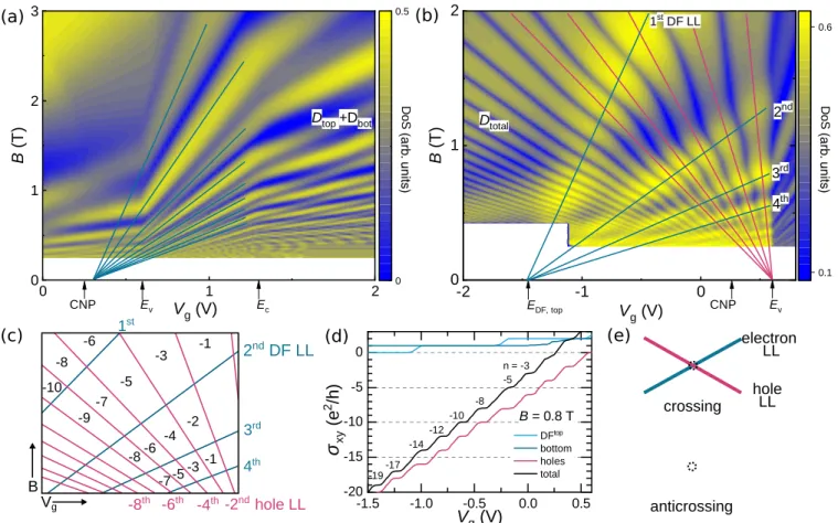
The most striking feature in transport and thus in the LL fan chart arises from coexisting surface electrons and bulk holes in regions 2 and 3 [see Fig.3(b)and magnification in Figs.5(b)and5(e)], each characterized by its own set of LLs.
Note that in the valence band both top and bottom surface electrons are present. However, only the top surface electrons participate in the formation of the observed oscillations. The
FIG. 5. (a)∂2σxx/∂Vg2forBup to 3 T andVg>0 covering the bulk gap and conduction band region. Dark blue lines retrace the Landau levels. The Landau fan in the gap betweenVg(EV) andVg(EC) has its virtual origin atVg=0.05 V and stems from the top surface electrons.
A distinct change of slope is observed whenEF enters the bulk bands atVg(EV) andVg(EC). This is due to the reduced filling rates of surface electrons in the bulk bands. The distortion of the Landau fan in region 4 at fields between 1 and 2 T is ascribed to the onset of quantization of the bottom surface electrons. (b)∂2σxx/∂Vg2forEF in the valence band, i.e., forVg<Vg(EV) andBup to 2 T. Landau fans stemming from bulk holes (red) and top surface electrons (black) coexist in this regime. Whenever a bulk hole LL crosses a surface electron LL, the total filling factor parity changes, resulting in a shift of the SdH phase. (c) Hall conductivityσxy(Vg) forB=0.4. . .5 T andEF in the bulk gap.
For smallBfields the plateau values of the individual traces increase with increasing field (dashed lines) due to superposition of quantized Hall conductivity from the top surface (constantσxy) and classical Hall conductivity of back surface electrons (σxylinear inVg). At higherB quantized steps appear. (d) The Hall conductivityσxy(Vg) measured in the valence band. In the region of the checkerboard pattern alternating sequences of plateaus with only odd or even filling factors (dashed lines) show up. The changes in filling factor parity stem from coexisting spin-resolved topological surface states and spin-degenerate bulk holes. (e) Enlarged region of coexisting electron and hole Landau levels of (b) showing the alternating sequences of even (odd) total filling factors.
bottom electrons have an extremely small filling rate (exper- imentally indistinguishable from zero) and therefore do not develop observable Landau fans. The electron Landau levels start from the Dirac point of the top surface electrons, marked byEDF,t opon the gate voltage scale of Fig.5(b), and fan out towards positive gate voltages. No signature of Dirac holes can be resolved at more negative gate voltages due to the increasing noise level. The (bulk) hole Landau levels, on the other hand, start at the valence band edgeEV [see Figs.2(a) and 5(b)] and fan out towards negative gate voltages. The simultaneous filling of the two sets of Landau levels results in the formation of a checkerboardlike pattern where minima and maxima alternate, clearly seen in the∂2σxx/∂Vg2color map of Fig.5(b). This checkerboard pattern is very similar to the one observed in InAs/GaSb based electron-hole systems [7]. The checkerboard pattern is connected to an anomaly in theσxy
traces taken for magnetic fields between 0.4 and 5 T, shown in Fig.5(d): In the curves measured between a magnetic field
of 1 and 2 T every second quantized plateau is missing; i.e., the filling factor of the plateaus changes by 2. Further, there are clear transitions in Fig. 5(d) between regions in which plateaus with either odd or even multiples of the conductance quantume2/hprevail.
The experimental observation suggests the picture pre- sented below to explain the checkerboardlike pattern in the fan chart and the unique odd-to-even plateau transitions.
Figure 6(c) displays a cartoon showing the coexisting electron-hole LLs together with the corresponding filling fac- tors. Both electrons and holes are characterized by a partial filling factorνi, counting the number of occupied electron and hole LLs. The total filling factorν (and the corresponding value ofσxyin units ofe2/h) is the sum of electron and hole filling factors, νeand −νh, respectively. Since the hole LLs are doubly (spin) degenerate,νh can only have even values in contrast to the topological surface electron, for which the filling factor increases in steps of 1 whenEF is swept across
FIG. 6. (a) Calculated partial DOS of top and bottom surface states (extracted from the full calculation described in the Appendix) near the bulk gap and forB 3 T. Yellow stands for high DOS values (i.e., LLs) while the blue color represents small DOS (i.e., the gaps between LLs).EV,EC,CNP, andEDF,toplabel points on the gate voltage axis, which were matched to experimentally obtained values. The observed LLs exhibit, as in experiment, pronounced kinks at the band edges (EV,EC) resulting from the abrupt change of the partial filling rates when bulk states get filled. (b) The calculated total DOS in the valence band, corresponding to the experiment shown in Fig.5(c)shows, for lowB, an unusual pattern stemming from the interplay of spin-degenerate hole LLs (red lines) and nondegenerate electron LLs (blue lines). Color code as in (a). (c) Sketch of the crossing electron (Dirac fermion) (blue) and hole LLs (red). WhenEF crosses a Dirac fermion LL, the filling factor changes by 1; when it crosses a hole LL it changes by 2. The black numbers give the resulting filling factors in between electron and hole LLs.
(d)σxyas a function ofVgcalculated for the different charge carrier fractions when degenerate and nondegenerate hole and electron LLs, as in (b), coexist. The total Hall conductivityσxy(black line) shows, as in experiment, the switching between odd and even plateau values, depending on the parity of the electron filling factor. (e) The simulations shown here only consider the electrostatics of the LLs resulting in degenerate LLs at crossing points. However, quantum mechanics requires that such crossings be avoided. This situation is sketched here to show that in our model LL crossings lead (incorrectly) to maxima in the DOS while in experiment such crossings are characterized by a reduced density of states at the crossing point (black circle).
an electron LL. Whether the total filling factor is even or odd therefore depends on the parity of νe. Figure6(c) illustrates this scenario: Between the third and fourth hole LL,−νh=
−6, while between the first and the second electron LL, νe=1. Added together, the total filling factor isν= −5. To understand the experimental result, yet another ingredient is needed. The rate at which electron and hole LLs are filled is greatly different. The values of the partial filling ratesdns/dVg
andd ps/dVg depend both onB andVg, while their sum, the total filling rate, is a constant given byC/e. Within a simple picture, the average value of the partial filling rates (averaging over the small oscillatory part) follows the zero magnetic field filling rates. The filling rate at B=0 is much smaller for surface electrons than for holes due to their lower density of states. This is directly shown by the experimental data in Fig.1(e)and the corresponding model in Fig.1(g)(see also Figs. S2(a) and S2(b) [30])whenEF is located in the valence
band. This also causes a different filling of electron and hole LLs. While for a gate voltage change of, say,Vg, a spin- degenerate hole LL with carrier density 2eB/hgets fully filled, an electron LL is still largely empty, or, viewing it the other way round: A change of the electron filling factorveby 1 is accompanied by changingνhby several even integers (due to the hole LL’s spin degeneracy). Within the picture developed above, we can readily explain the experimental observation:
A sequence of quantum Hall steps with only odd quantized step occurs, e.g., when the Fermi level stays between the first and second electron LL while it crosses several hole LLs as Vgis varied. WhenEF crosses an electron LL the parity of the filling factors changes and an even sequence of quantum Hall steps emerges. The switching between even and odd plateau sequences is direct proof that the surface states are topological in nature: With conventional spin-degenerate electron states, only Hall conductances with even multiples of e2/h would
appear in experiment. The checkerboard pattern in σxx is a consequence of the joint filling factor. Minima inσxx occur at integer total filling factors, corresponding to the dark blue regions in Figs.5(b)and5(e). These minima develop inside the quadrilaterals formed by the electron and hole LLs; see, e.g., Fig.6(c). Figures6(b)and6(d)show model calculations which confirm the arguments presented above and reproduce the peculiar pattern in σxx and σxy. Figure 6(d) displays calculatedσxy traces for the different charge carrier species in the system. The total Hall conductivity at constant B= 0.8 T displays, as in experiment, transitions from odd to even sequences of quantum Hall steps. Further, the calculated fan chart in Fig. 6(b) reproduces qualitatively the checkerboard pattern observed in experiment. We highlight in this fan chart the electron and hole Landau levels. Each of the quadrilaterals contains an integer total filling factor. There is, however, one obvious difference between experiment and calculation: At the crossing points of the LLs in Fig.6(b) the total density of states is highest, reflected by the bright yellow color. In the experiment shown in Fig. 5(b), in contrast, the value of the conductivity at the crossing points of electron and hole LLs is between maximum and minimum values. The reason is that we ignore anticrossings in our model. The anticrossing of LLs reduces the density of states at the crossing points and thus the conductivity. The cartoon in Fig.6(e)shows the idealized LL crossing assumed in our simplistic model compared to a more realistic one.
At higher magnetic fields, beyond the first electron LL, the checkerboard pattern disappears and the regular fan chart of the total charge carrier density, which emanates from the charge neutrality point, develops. Above about 3 T the spin degeneracy of the bulk holes starts to get resolved. This is shown in more detail by Fig. S3(a) in the Supplemental Material [30].
VII. CONDUCTION BAND
In the conduction band, labeled as region 5 in the Fig.3(b), the system has common features both with the gap and the VB. Again, bulk and surface carriers coexist in the con- ductance band. However, the differences in effective masses and filling rates between bulk and surface carriers are much smaller than on the valence band side. In addition, the con- tribution of bulk carriers to the conductivity is smaller than that of the surface states, which is in contrast to the VB. And, very importantly, the charge sign is the same, resulting in the same direction (i.e., towards positive gate voltages) of the LL fan charts. Nonetheless, due to the coexistence of quantized top surface, bottom surface, and bulk electrons an intricate structure of SdH oscillations develops and several Landau fan charts develop. First, the fan chart associated with LLs of the conduction band (bulk) electrons in Fig. 3(b), which emerges at EC, fans out to the right, and crosses the LLs of the top surface electrons, which is clearly visible. The corresponding fan is also shown and magnified in Fig. S4(d) in the Supplemental Material [30].
Further, one can identify the Landau chart which originates from the CNP and reflects the total filling factorν, i.e., the sum of all electrons in the system. These Landau levels dominate
at high magnetic field and are the reason why high-field SdH oscillations reflect the total carrier density. The corresponding LL fan is highlighted in Fig. S4(b) in the Supplemental Material [30]. The third chart, which dominates at lower B and echoes the density of the top surface electrons, is shown in Fig. S4(c) [30]. The fan chart originates from the virtual point of zero density of the top surface. One would expect a fourth chart associated with the bottom surface electrons;
the intermixing of LLs in this regime prevents its clear ob- servation in Fig. 3(b). Apart from the complex oscillation pattern, the anomalies due to the interplay of odd and even filling factors are also expected in this region: When bulk electrons (doubly degenerate) and Dirac surface electrons (nondegenerate) coexist, we expect, as in the valence band, even-odd transitions of the quantized Hall plateaus. Indeed, we see even-odd switching in Fig. S3(b) [30], but due to the large filling factors the signature is less pronounced as in the case of coexisting electrons and holes.
VIII. SUMMARY
In this work, we studied Shubnikov–de Haas oscillations and the quantum Hall effect under the peculiar conditions of a two-dimensional gas of Dirac fermions “wrapped” around the 80-nm-thick bulk of a strained HgTe film. The interplay of four different carrier types, i.e., bulk electrons and holes, as well as top and bottom surface Dirac electrons leads to an intricate pattern of the Landau level fan charts. We identified six different regions in the charts, which differ in terms of condition (low or quantizing magnetic field) and types of charge carrier which coexist at the Fermi level. The latter is tuned by means of the applied gate voltage. A simple model based on the superposition of conductivities and densities of states connected to the different subsystems enables us to describe all chart regions as qualitatively correct. In partic- ular, a two-component Drude model fits the system in weak magnetic fields. The opposite limit of strong magnetic fields is characterized by the QHE state and resolved LLs, where the total charge density defines the position of longitudinal con- ductivity minima and plateaus in Hall conductivity. In inter- mediate magnetic fields, the system becomes highly sensitive to the exact position of the Fermi level. In the valence band, we discovered periodic transitions from even to odd filling factors, which we associate with interacting spin-degenerate holes and nondegenerate surface electron LLs. We found similar, but less marked behavior in the conduction band. In the bulk energy gap, the nature of SdH oscillations is mainly determined by LLs stemming from electrons on the upper surface sitting on a monotonous background conductivity of semiclassical electrons on the bottom surface. The onset of bulk Landau levels observed atEcin Fig.3(b)directly shows that the Fermi level, in contrast to previous claims, can be easily tuned into the conduction band [12]. Though we use high-mobility strained HgTe as a model system, we note that our conclusions and analyses are valid for a wide class of topological insulators, e.g., Bi-based ones, even if those show, due to their significantly higher disorder, usually much less resolved quantum transport features.
ACKNOWLEDGMENTS
The work was supported by the Deutsche Forschungsge- meinschaft (within Priority Programme SPP 1666 “Topologi- cal Insulators”), the Elitenetzwerk Bayern Doktorandenkolleg (K-NW-2013-258, “Topological Insulators”), and the Euro- pean Research Council under the European Union’s Horizon 2020 research and innovation program (Grant Agreement No.
787515, “ProMotion”). D.A.K. acknowledges support from the Russian Scientific Foundation (Project No. 18-72-00189).
APPENDIX: COMPUTER SIMULATION OF LANDAU LEVEL FILLING
In order to explain the LL fan charts and the Hall step pattern, obtained from σxx and σxy data, we developed a model which qualitatively describes the system consisting of several groups of carriers in both weak and quantizing magnetic fields and at zero temperature. Within the model, each group of carriers gives an independent contribution to the total charge of the system, its conductivity σxx andσxy, and density of states D, and is characterized by a set of constant (charge, effective mass etc., see TableI) and variable (density, Fermi energy, the band edge, etc.) parameters. The different groups of carriers are linked via the common Fermi level and electrostatic coupling. In a magnetic field each group generates a set of Landau levels which are filled up to the Fermi level (at T =0), whose position in turn depends on the charge carrier density. The input of the calculation are gate voltage Vg and magnetic field B, while the output are both partial and total filling factors, the densities of states (DOS) Di, and Hall conductivities σxyi for particular B and Vg values. The detailed description of the model follows.
Depending on the gate voltage, up to four groups of charge carriers are present in the system, namely, top and bottom Dirac surface electrons, bulk electrons (conduction band), and bulk holes (valence band), marked by the indices top, bot, b (bulk) and h (holes) below. Each of these groups is characterized by a parabolic two-dimensional dispersion law with an effective mass ofmi (values used in the calculation are listed in TableI). This approach neglects the quasilinear Dirac dispersion of the surface states but is justified as we seek qualitative understanding rather than full quantitative agreement. Next, each group is characterized by its lowest energy Eci (Dirac point for top and bottom electrons, con- duction band edge for bulk electrons) and valence band edge Ev (for holes). The electron (hole) density in each group readsnsi = ∫EEFi
c Di(E)dE[ps= ∫EEvFDh(E)dE]. While at zero magnetic field the constant DOS is given byDi= 2πgismh¯i2 with gis the spin degeneracy and ¯h the reduced Planck constant, at nonzeroB Landau levels emerge, described by a sum of Gaussians with linewidth i:
Di(E)= gLL i√ π
∞
n=0
e−(E−E in)
2
2 .
Here gLL=eB/h is the spin-resolved LL degeneracy and En the energy of the nth LL. For surface carriers, LLs are spin resolved and Eni =Eci+hω¯ ci(n+12),with ωic=eB/mi
the cyclotron frequency. For bulk carriers each LL is initially doubly degenerate, but the degeneracy is lifted due to Zeeman splitting,iZ =g∗iμBB, whereg∗i is the Landégfactor of bulk carriers (see Table I). Thus, for bulk electrons,En±=Ecb+ hω¯ cb(n+12)±2bZ and for holes, En±=Ev−hω¯ hc(n+12)±
hZ
2 holds.
The electrostatics of the system is introduced in the same way as done in our previous work [23], but extended to the case of quantizing magnetic fields. The key point is that each group of carriers is exposed to the electric field of the others and the changes of a group’s carrier density create an electrostatic energy shift for the others. Each group is treated as an infinitely large, charged capacitor plate of zero thickness with charge density i= −enis (eps for holes), located at certain distances from the gate [see Fig.1(f)]. Every charged plate induces a symmetric electric fieldF=i/2εε0on both sides of the plate, which, in turn, creates an electrostatic energy shift for the other groups of carriers. On the other hand, the electric field below the bottom surface is zero. Therefore, the charge on the bottom surface creates an electric field of enbots /εHgTeε0 inside the HgTe layer, where ε0 is the electric vacuum permittivity andεHgTe=80, the effective (see below and “Limitations of the model” section) dielectric constant of HgTe. Then, the electrostatic energy shift for a layer located in a distanced from the bottom is e2nbots d/εHgTeε0. In our model, a change of the electrostatic energy shifts the position of Eci and Ev. The energy shift for bulk carriers is solely determined by the charge on the bottom surface (because in the model there are no other carriers in between), while the top surface electrons are affected by both bottom surface electrons and bulk carriers with weights proportional to the respective distance. Note that the electrostatic approach used here is fully equivalent to the capacitance model used in our previous work [23], and in the limit of small magnetic fields both models give the same values for the partial densities.
Due to the common Fermi level, the electrostatic energy shift couples densities of different groups of carriers and results in screening of the electric field induced by the top gate. For the simplest case whenEF is in the gap (i.e., only surface electrons exist) an increase ofnbots bynbots is accom- panied by a simultaneous shift ofEF byEF =nbots /Dbot andEctop by−e2nsbotd/εHgTeε0; finally one obtainsntops = nbots (1+e2d/εHgTeε0Dtop), assuming Dbot =Dtop for sim- plicity. The dielectric constant of the HgTe layer was chosen in a way to agree with the partial filling rate of top and bottom surface electrons, found in experiment. To the same end, the (average) spatial location of bulk electrons and holes was taken as a fitting parameter (see TableI). In order to agree not only with filling rates, but also with the experimentally extracted carrier densities, an additional constant energy shift was introduced for each group except the one on the bottom surface (which is chosen as a reference).
The calculation procedure was as follows: First, for a specifiedVgvalue the total charge in the system is calculated by the linear relation Q= −αe (Vg−VgCNP), where α= C/e=2.42×1011cm2/V s is the total filling rate. Next, for a given value of the magnetic field the densities of states of the different carrier speciesDi(E) are calculated analytically taking the electrostatic energy shifts into account. Finally,
the equation Q=eps(EF,Ev)−e
inis(EF, Eci) is solved numerically giving the values ofEF,nis, andpsas an output.
With these values the partial densities of states andσxywere calculated and plotted in Fig.6.
At zero magnetic field, there is a linear relation between the partial densities [see Fig.1(g)] leading to constant filling rates in certain gate voltage regions. However, screening works differently in the limit of strong magnetic fields when the sep- aration between neighboring LLs, stemming from arbitrary carrier types, becomes large enough. In this case, the gate in- duced change of the total chargeQis not shared between the different “capacitor plates” (carrier species) according to the zero-field partial filling rates, but all the charges are filled into the layer which has a (well-separated) LL located at the Fermi level. Consider, e.g., EF in the gap between two LLs, one belonging to the top, the other to the bottom surface electrons.
In the case whenEF is tuned (viaBorVg) into the LL of the top surface a full screening scenario is realized: All additional carriers go to the top surface (Q=qntop) and no electric field penetrates the HgTe film since it is screened by the top surface electrons. In the opposite case, whenEF is tuned into the bottom LL, screening is absent: All new carriers are added to the bottom surface (Q=qnbot) and the electric field penetrates the HgTe film without attenuation. In our electro- static model, the top surface is subjected to an electrostatic energy shift of −eQd/εHgTeε0. However, if the distance from EF to the next LL is larger than this energy shift, all newly added electrons will still go to the bottom surface only.
In the limit of strong magnetic fields, the partial filling rates for every group of carriers may only take two values: 0 when the LL of the corresponding carrier species is not atEF and 1 if the associated LL is atEF. Our model does not describe the detailed transition between the small and strong magnetic field limit. However, the strong field limit in our system can be clearly seen in the QHE data shown in Figs.3(a)and3(b).
Limitations of the model
As stated before, the model was developed in order to achieve qualitative agreement with the experimental data, but, surprisingly even semiquantitative concordance is achieved in some regions. In particular, the DOS oscillations in the bulk energy gap fit the experimentally obtained conductivity oscillations well. Excellent agreement is also achieved in the limit of strong magnetic fields. The main benefit of the model is that it explains conclusively—with utmost simplicity—
the observed magnetotransport peculiarities. However, the model has a set of built-in limitations, which are described below:
(1) The real band dispersion at zero magnetic field is replaced for all kinds of carriers by a parabolic one. This re- duction is justified, because the QHE is of fundamental nature and only slightly depends on the details of the band structure.
The observed magnetotransport features are explained by the interplay of the LLs of different charge carriers, taking the system’s electrostatics and LL broadening due to disorder into account. Using the real band structure will simply lead to a renormalization of the broadening parameters but does not lead to any new physics. We note that the use of a parabolic dispersion significantly simplifies the model.
(2) The effect of the out-of-plane electric field on the electronic band dispersion, expected in thin HgTe films [19], is neglected. One of the main consequences of the band distor- tion is a reduced partial filling rate for the bottom side surface electrons (and an increased one for top surface electrons, accordingly). In order to fit the experimentally obtained filling rates, we have therefore to use an effective dielectric constant of the HgTe layer ofεHgTe=80, which is larger than the real one of about 20.
(3) No quantum mechanical interaction between LLs is taken into account. When two LLs (stemming from bulk holes and surface electrons, e.g.) cross, a maximum in the DOS forms in our calculations. In a more realistic scenario, the interaction between carriers should lead to an anticrossing of LLs and reduced values of the DOS and the longitudinal con- ductivity at the crossing. Consequently, we cannot reproduce all details of the checkerboard pattern shown, e.g., in Fig.5(b).
(4) In the limit of strong magnetic fields, the experimen- tally measured width of the conductivity peaks is smaller than the width of the gap region on the gate voltage scale.
In contrast, our DOS calculations show minima and maxima regions of similar width. This is a well-known discrepancy, which is due to the fact that (i) the conductivity in the quantum Hall regime is proportional to the square of the Landau level DOS [2], and that (ii) effects which stem from transport in edge states (parallel to the applied field) are not taken into account.
(5) The valley degeneracy of bulk holes is neglected. Band structure calculations predict a fourfold degeneracy for (100)- oriented HgTe films and QWs and a twofold one for (013)- oriented ones, used here. There has been difficulty observing the valley degeneracy in experiment. Some authors believe that the valley degeneracy is lifted because of the Rashba effect [37].
(6) Effects of the Berry phase which give rise to a phase shift of the quantum oscillations, and which we observed in our material system before [13,23], are neglected here.
[1] K. V. Klitzing, G. Dorda, and M. Pepper,Phys. Rev. Lett.45, 494 (1980).
[2] T. Ando, A. B. Fowler, and F. Stern,Rev. Mod. Phys.54, 437 (1982).
[3] R. Dingle, H. L. Störmer, A. C. Gossard, and W. Wiegmann, Appl. Phys. Lett.33, 665 (1978).
[4] K. S. Novoselov, E. McCann, S. V. Morozov, V. I. Fal’ko, M. I.
Katsnelson, U. Zeitler, D. Jiang, F. Schedin, and A. K. Geim, Nat. Phys.2, 177 (2006).
[5] E. E. Mendez, L. Esaki, and L. L. Chang,Phys. Rev. Lett.55, 2216 (1985).
[6] K. Suzuki, K. Takashina, S. Miyashita, and Y. Hirayama,Phys.
Rev. Lett.93, 016803 (2004).
[7] M. Karalic, C. Mittag, S. Mueller, T. Tschirky, W. Wegscheider, K. Ensslin, T. Ihn, and L. Glazman,Phys. Rev. B99, 201402 (2019).
[8] M. Z. Hasan and C. L. Kane, Rev. Mod. Phys. 82, 3045 (2010).