Probing the Coulomb gap in the topological insulator BiSbTeSe2 via Quantum Capacitance
Jimin Wang,1 Cosimo Gorini,2 Klaus Richter,2 Zhiwei Wang,3, 4 Yoichi Ando,3 and Dieter Weiss1
1Institute of Experimental and Applied Physics, University of Regensburg, 93040 Regensburg, Germany
2Institute of Theoretical Physics, University of Regensburg, 93040 Regensburg, Germany
3Physics Institute II, University of Cologne, Z¨ulpicher Str. 77, 50937 K¨oln, Germany
4Key Laboratory of Advanced Optoelectronic Quantum Architecture and Measurement, Ministry of Education, School of Physics,
Beijing Institute of Technology, Beijing, 100081, China (Dated: December 6, 2019)
Abstract
BiSbTeSe2 is a 3D topological insulator with Dirac type surface states and low bulk carrier density, as donors and acceptors compensate each other. Dominating low temperature surface transport in this material is heralded by Shubnikov-de Haas oscillations and the quantum Hall effect. Here, we experimentally probe the electronic density of states (DOS) in thin layers of BiSbTeSe2 by capacitance experiments both without and in quantizing magnetic fields. By probing the lowest Landau levels, we show that a large fraction of the electrons filled via field effect into the system ends up in (localized) bulk states and appears as a background DOS. The surprisingly strong temperature dependence of such background DOS can be traced back to the Coulomb gap in the system.
arXiv:1912.02725v1 [cond-mat.mes-hall] 5 Dec 2019
An ideal three-dimensional (3D) topological insulator (TI) has an insulating bulk, char- acterized by a gap in the energy spectrum, and symmetry protected, conducting surface states (1,2 and references therein). As these helical surface states are not spin degenerate, 3D-TIs provide a promising platform to realize topological superconductivity, a prerequi- site to search, e.g., for Majorana zero modes3,4. Experimentally available TIs like Bi2Se3 or Bi2Te3 are, however, far from ideal as they feature, due to intrinsic defects, a relatively high electron or hole density larger than 1018 cm−3 (see5 and references therein). By com- bining p-type and n-type TI materials, i.e., by compensation, the bulk concentration can be suppressed2,6. This comes at the price of large potential fluctuations at low tempera- tures as the resulting ionized donor and acceptor states are poorly screened and constitute a randomly fluctuating Coulomb potential, bending the band edges and creating electron and hole puddles7,8. These were observed by, e.g., optical spectroscopy5. In the absence of metallic surface states, i.e., in fully compensated conventional semiconductors, variable range hopping governs low-temperature transport (T < 100 K)9. Recently, Skinner et al.
have shown that the electronic density of states (DOS) in the bulk is nearly constant un- der these circumstances and features a Coulomb gap at the Fermi level µ7,8. In 3D-TIs, in addition, Dirac surface states, which form a two-dimensional (2D) electron (hole) system, encase the bulk and constitute the dominating transport channel at low temperatures.
Here, we explore the interplay between topological surface and trivial bulk states. To this end we probe the DOS of the Dirac surface states by capacitance spectroscopy. The total capacitanceC, measured between a metallic top gate and the Dirac surface states, depends on the geometric capacitance per unit area, C0 = 0/d, and on the quantum capacitance e2D(µ),
C−1 =C0−1+
e2D(µ)−1
. (1)
Here, d are, respectively, dielectric constant and insulator thickness,0 the vacuum dielec- tric constant, andD(µ) the DOS at the Fermi level (chemical potential)µ. The quantum ca- pacitance, connected in series toC0, reflects the energy spectrum of 2D electron systems10–12, and probes preferentially the top surface DOS in 3D-TIs13. At higher temperatures, D has to be replaced by the thermodynamic density of states (TDOS) at µ, D(µ) = dn/dµ, with n the carrier density. While gating of 3D-TI and tuning of the carrier densities of top and bottom surfaces has been explored in the past14,15, the quantum capacitance and the DOS in a compensated TI like BiSbTeSe2 remained uncharted. Our measurements show that, while
Dirac surface states dominate low-T transport as expected, the bulk provides a background of Coulomb glass type, capable of absorbing a large amount of charge carriers. These missing charges is very common in 3D-TI transport experiments, yet to the best of our knowledge unexplained16–19.
We used pristine, slightly p-doped BiSbTeSe2 crystals grown by the modified Bridgman method6. Angle-resolved photoemission spectroscopy has demonstrated that Dirac point and µ of this material lie in the bulk gap20. BiSbTeSe2 flakes were exfoliated onto highly p-doped Si chips (used as backgate) coated by 285 nm SiO2. The flakes were processed into quasi-Hallbars with Ti/Au (10/100 nm) ohmic contacts. A larger h-BN flake, transferred on top of BiSbTeSe2 serves as gate dielectric. Finally, we use Ti/Au (10/100 nm) as a top gate contact. Fig. 1(a) and 1(b) display the layer sequence and optical micrograph of one of the devices, respectively.
Transport measurements using low ac excitation currents (10 nA at 13 Hz) were carried out between 1.5 K and 58 K and in magnetic fields B up to 14 T. Temperature dependent measurements show (see Fig. S1 in21) that at 1.5 K transport is entirely dominated by the surface with negligible contribution from the bulk. The carrier density and µ of top and bottom surfaces can be adjusted by top and bottom gate voltages,Vtg, Vbg, respectively. This is shown for the Hall resistivity at 14 T in Fig. 1(c). The device displays well developed quantum Hall plateaus at total filling factor ν = -1, 0 and 122. The plateaus are well separated from each other and marked by dashed purple lines. As these lines run nearly parallel to the Vtg- and Vbg-axes, respectively, we conclude that the carrier density on top and bottom can be tuned nearly independently.
Capacitance measurements – We use a two-terminal setup with one contact connected to the top gate, the other to the BiSbTeSe2 layer, see inset in Fig. 1(d). A high-precision capacitance bridge AH2700 with ac modulation of 0.1 V was used at the lowest operation frequency of 50 Hz to suppress resistive effects13. To minimize hysteresis, we always sweep Vtg in one direction only. Figure 1(d) shows the measured capacitance C, which is directly connected to the DOS, see Eq. (1). The measured trace with a minimum at the Dirac or charge neutrality point (CNP) resembles the quantum capacitance measured for graphene, apart from a pronounced electron-hole asymmetry12,23,24 due to a parabolic contribution to the linear E(k) dispersion25. Explicitly, the latter reads E = }vFk + }2k2
2m∗, with ~ the reduced Planck constant,vF the Fermi velocity at the Dirac point, andm∗ the effective mass.
(a)
(c) (d)
0 1
-1 0
surface states Ti/Au (Top gate)
h-BN (30 nm) BSTS (67 nm) SiO (285 nm)2
Si (p++, Back gate)
~~ ~~
~~ ~~
~~
~~
B = 0, T = 1.5 K Experiment Fit E
k D(E)
E
Ti/Au h-BN BSTS Vac+Vdc
-3 -2 -1 0 1 2 3
4.58 4.60 4.62 4.64 4.66 4.68
C (pF)
Vtg-VCNP (V) Vbg (V)
4 2 0 -2 -4
-20 -10 0 10 20
V (V)tg
(b)
FIG. 1. (a) Design of layer sequence. Red lines sketch the topological surface states. (b) Optical micrograph of the device. The dashed yellow line marks the capacitor area of 1.8×103µm2. (c) ρxy as function ofVtg andVbg, respectively, atT = 1.5 K andB = 14 T. The almost horizontal and vertical dashed purple lines separate the region of well developed QHE with total filling factors of -1, 0, and 1 (unit h/e2), from regions of higher filling factors. (d) C(Vtg) at T = 1.5 K and B = 0 T. The pronounced minimum reflects the bulk gap. For better comparison, the CNP of all measurements is shifted to zero via VCNP. The red line is a fit using a Gaussian broadening of the Fermi level with σ = 29.4 meV (see text). To compare with experiment we added a parasitic capacitance of∼3.07 pF. The lower left inset illustrates the measurement principle, the upper inset the energy dispersion of the surface states in the bulk gap (left) and the corresponding DOS (right).
It is sketched in the upper inset of Fig. 1(d), together with the electron-hole asymmetric, nearly E-linear DOS, given by D(E) =
m∗(Ω−m∗vF) 2π}2Ω
. Here we used that k = √
4πn and Ω =p
(m∗vF)2+ 2Em∗.
While in a perfect system D(E) vanishes at the CNP, disorder smears the singularity, as in case of graphene12. We model the potential fluctuations by a Gaussian distribution of en- ergies with widthσ, resulting in an average DOShD(µ)i=R∞
−∞D(E)√1
2πσexp−(E−µ)2 2σ2
dE.
To convert energies into voltages we use n =C0(Vtg−V0)/e, with e the elementary charge and V0 describing n at zero voltage. By fitting hD(µ)i to the data in Fig. 1(d) we extract σ = 29.4 meV,vF = 3.2·105m/s andm∗ = 0.47m0 (m0 = free electron mass). The broaden- ing σ is only important in the immediate vicinity of the CNP but hardly affects the values of vF and m∗. The obtained vF and m∗ values agree well with ARPES data14,20 and values extracted from Shubnikov-de Haas oscillations25.
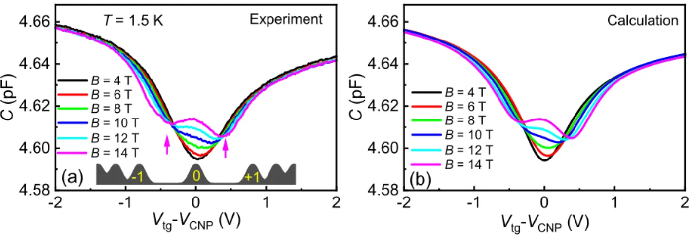
B-field dependence of capacitance measurements – Our key result arises when we crank up the magnetic field and measure signatures of the Landau level (LL) spectrum, shown in Fig. 2(a). At the 0-th LL level position a local maxima emerges with increasing B-field, flanked by minima at each side. The two minima, highlighted by arrows, correspond to the Landau gaps between LLs 0, and±1 [see Fig. 2(a)]. Due to the large broadening, higher LLs do not get resolved. Lowering T down to 50 mK does not resolve more structure, indicating that disorder broadening is the limiting factor. By sweeping Vtg across the 0-th LL, i.e., from arrow position to arrow position, the carrier density changes by the LL degeneracy
∆n = eB/h. In contrast, the change of carrier density ∆n, calculated via capacitance,
∆n= Ce0∆Vtg, is by a factor 1.4 higher. Hence, we must assume that a large fraction of the carriers, induced by field effect, ends up in the bulk and is localized at low T.
To compare with these experiments we calculate C(Vtg) using Gaussian-broadened LLs, DLL(E) = √2πΓ1 eBh P
exp−(E−En)2 2Γ2
, with broadening Γ. The LL spectrum dispersion reads26
En=|n|~eB
m∗ + sgn(n) s
~eB 2m∗
2
+ 2eB~vF2|n|, (2)
with n = 0, ±1, ±2, . . ., and the tiny Zeeman splitting was neglected. Using the above DOS is insufficient to describe the data - the distance ∆Vtg between adjacent Landau gaps (marked,e.g., by arrows in Fig. 2(a) for the 14 T trace) is too small21. ∆Vtg is the voltage needed to fully fill the 0-th LL of the surface states. Since ∆Vtg in experiment is larger than calculation (relies on the filling rate dn/dVtg ≈ C0/e), it means that a fraction of the field-induced electrons does not go to the surface states but eventually into the bulk. Thus a higher voltage (higher δn) is needed to fill the zeroth LL. On contrast, we obtain almost
Calculation Experiment
T = 1.5 K
0 +1 (b) (a) -1
-2 -1 0 1 2
4.58 4.60 4.62 4.64 4.66
C (pF)
Vtg-VCNP (V)
B = 4 T B = 6 T B = 8 T B = 10 T B = 12 T B = 14 T
B = 4 T B = 6 T B = 8 T B = 10 T B = 12 T B = 14 T
-2 -1 0 1 2
4.58 4.60 4.62 4.64 4.66
C (pF)
Vtg-VCNP (V)
FIG. 2. (a) C(Vtg) for B ranging from 4 T to 14 T. The lower inset sketches the LL DOS for LLs -1, 0 and 1. Arrows mark the position of the Landau gaps for the 14 T trace21. (b) Model calculations to (a) based on Eq. (3) after adding a parasitic capacitance of ∼3.06 pF. Parameters of the fit at 1.5 K: Γ = 14.9 to 15.9 meV;Db = 2.4·1035m−2J−1.
perfect agreement – see Fig. 2(b) – if we introduce an energy-independent background DOS Db which models these bulk states21. The calculated TDOS we compare with experiment thus reads
D(µ) = Z ∞
−∞
[DLL(E) +Db]∂f
∂µdE, (3)
with f =f(E−µ, T) the Fermi function.
As shown in Fig. 2(b), the constant background Db leads to excellent agreement with experiment. Although the bulk DOS is hardly directly accessible by the quantum capacitance itself (i.e., by its value), we probe it indirectly via the missing charge given by the Landau gap positions. This missing charge carrier issue holds also for the quantum Hall trace in Fig. 1(c), where ∼30% of the induced electrons are missing. Indeed, it also appears in several other publications with missing electron fractions ranging from 30% (as here) to 75% (see16–19).
The bottom line is: The change of surface carrier density extracted from the Landau gap positions is smaller than the one ”loaded” into the system within the same voltage interval. Further, the filling rate dn/dVtg determined by the classical Hall effect at 1.5 K is consistent with the one found for the surface states21. Thus, the charge carriers loaded at low T into the bulk are localized and do not contribute to transport. This is consistent with transport experiments16,27, and also in line with what is expected in fully compensated
(c) (d) (b)
0 10 20 30 40 50 60
0 4 8 12 16 20
Dd (T) (1035 J-1 m-2 )
T (K)
tg
B = 14 T Calculation 1.5 K
4.4 K 20 K 39 K58 K
-3 -2 -1 0 1 2 3
4.55 4.60 4.65 4.70
C (pF)
V -VCNP (V)
(a)
B = 14 T Experiment DV
1.5 K 4.4 K 20 K 39 K 58 K
-3 -2 -1 0 1 2 3
4.55 4.60 4.65 4.70
C (pF)
Vtg
tg
tg
-VCNP (V)
0 10 20 30 40 50 60
0.8 1.2 1.6 2.0 2.4
DV (V)
T (K)
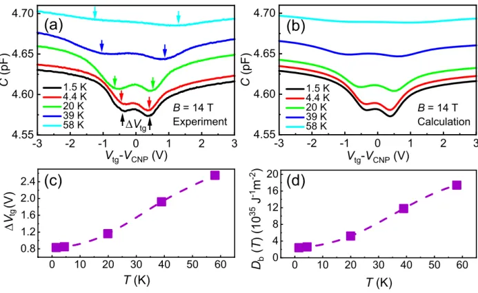
FIG. 3. (a) C(Vtg) at B = 14 T for various Ts. Arrows mark the minima corresponding to Landau gaps. For increasing T the voltage difference ∆Vtg between adjacent gaps increases. The trace at 1.5 K was shifted down by 0.032 pF for clarity. (b) Calculated C(Vtg) using Eq. (3) with Db values in (d), and Γ = 13−15.2 meV. (c) ∆Vtg vs. T. (d) ExtractedDb.
semiconductors9, as was recently highlighted in Ref.7. There, bulk transport of compensated TI was considered, where local puddles of n- and p-regions form. In this regime, low-T transport is governed by variable range hopping, the DOS within the gap is essentially constant, while filled and empty states are separated by the Coulomb gap atµ7,9.
Using a constant background affects somewhat the values extracted above fromC(Vtg, B = 0). Thus, we fitted the trace in Fig. 1(d) using the same Db = 2.4·1035 m−2J−121. Now a reduced broadening σ = 15 meV is needed. C(Vtg) is then best described by slightly modified values: vF = 2.8·105m/s and m∗ = 0.57m0, respectively, still compatible with results reported elsewhere14,20,25.
Temperature dependence of quantum capacitance – The background DOS rises quickly with temperature. Corresponding C(Vtg) data for 14 T and various Ts up to 58 K is shown in Fig. 3(a). The local minima due to Landau gaps, marked by arrows, shift with increasing T to largerVtg. The corresponding ∆Vtg(T) is shown in Fig. 3(c). For fixed B the Landau
degeneracy eB/h is constant and does not depend on temperature. The increasing ∆Vtg needed to fill the 0-th LL of the surface states thus indicates that, with increasing T, more carriers are lost to the bulk. Similar behavior was found for quantum Hall data16,27. Clearly, to model the Landau gap positions correctly, a strongly T-dependent TDOS is required. A simple approach consists in introducing a T-dependent background DOS, Db →Db(T). Its values used to fit the data of Fig. 3(a) are shown in Fig. 3(d); the resulting C(Vtg) traces for different temperatures are plotted in Fig. 3(b). Db is nearly constant at low T but rises quickly at higher temperatures. However, a problem with this procedure is that for non- interacting electrons the number of single-particle states in a given energy (voltage) window by definition does not depend on T. The corresponding TDOS can still be T-dependent, but only as long as the tails of ∂f /∂µ, can reach regions with substantial changes of the single particle DOS, typically close to gap edges28. Yet the strongly temperature-dependent signal is obtained by scanning Vtg deep into the BiSbTeSe2 gap, whose width of 300 meV is far too large to explain the observations.
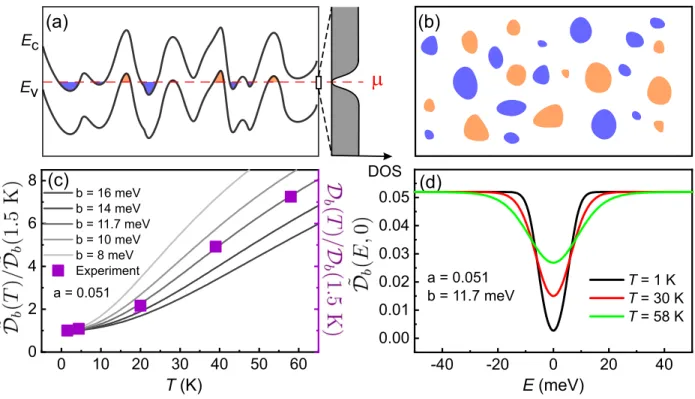
Probing the Coulomb gap – A way out of this apparent dead-end is provided by the strongly fluctuating potential landscape of compensated TIs like BiSbTeSe2, sketched in Fig. 4(a)-(b), where Coulomb interaction dominates7: In a nutshell, the background DOS emerges as an effective single particle DOS describing the ensemble of strongly interacting electrons filling bulk impurity states. As such, it is actually a µ- and T-dependent object, Db → Db(E, µ, T), characterized by a Coulomb gap at E = µ9. The TDOS we compare in Fig. 4(c) with experiment is then given by Db(µ) = ∂µ∂ R
Db(E, µ, T)f(E−µ)dE. Since both Db and the Fermi function f depend on µ, the derivative with respect to µ generates two terms:
Db(µ) = Z
Db∂f
∂µdE+ Z
f∂Db
∂µ dE. (4)
To describe the experiment we need to assume that the Coulomb gap cannot instantaneously follow µ if the carrier density is, as in our capacitance experiments, modulated by 50 Hz.
The Coulomb gap stems from rearrangement of unscreened charges in a strongly disordered landscape, and its formation time depends on disorder strength and type, temperature, and magnetic field29–31. Indeed, the electronic many-body system is known to behave as a Coulomb glass, characterized by long reaction/relaxation times32. Determining the exact shape and temperature dependence of the Coulomb gap DOS is a complex problem, whose details are still under debate33–38, and which is here further complicated by the presence of
DOS Ec
Ev m
(b) (a)
(c)
0 10 20 30 40 50 60 0
2 4 6 8
a = 0.051 b = 16 meV b = 14 meV b = 11.7 meV b = 10 meV b = 8 meV Experiment
T (K)
(d)
-40 -20 0 20 40
0.00 0.01 0.02 0.03 0.04 0.05
T = 1 K T = 30 K T = 58 K a = 0.051
b = 11.7 meV
E (meV)
FIG. 4. (a) Conduction (Ec) and valence band (Ev) profiles, fluctuating due to long range Coulomb interactions. A sketch of the bulk DOS including the Coulomb gap at µ is shown at right. The DOS at µ is probed in experiment. (b) Sketch of electron and hole puddles in the µ plane, consequence of the strongly fluctuating band edges in (a). (c) Comparison of calculated and measured D(T). Filled squares are experimental data. Different curves are model results for different values of the parameter b in Eq. (5). All curves are normalized to their values at T = 1.5 K. The TDOS grows by approximately a factor 8 betweenT = 1.5 K andT = 58 K. Such a relative increase is perfectly reproduced for a= 0.051, b = 11.7 meV. The best fit values lead to the TDOS associated with the Coulomb gap shown in panel (d) for different temperatures. Here, µis at zero energy.
topological surface states39.
On the time scale of 20 ms, set by the experiment, the Coulomb gap very likely cannot follow µ, i.e. Db is only a function of E for these short times at fixed T. Hence, the second term on the right hand side of Eq. (4) vanishes. On the other hand, the timescale of about 1 minute needed to produce each data point after changing Vtg should be sufficiently long to form a gap, at least partially. As the precise time scales for BiSbTeSe2 are not known, we resort to simple DOS models to test the feasibility of our approach.
For a qualitative understanding of our experimental data, it suffices to consider a bare- bone model for the bulk DOS, given in normalized form
D˜b(E, µ) =
tanhh
a+ E−µb 2i R dE0 tanhh
a+ E0b−µ2i .
(5)
Eq. (5) describes a T-independent Coulomb gap, whose (small) residual value at E = µ is determined by the dimensionless parameter a1, while b (with dimension of energy) fixes its width. The form is chosen so that forE →µit reproduces the known 3D Efros-Shklovskii form ∝ (E −µ)2, with the addition of a residual value. The corresponding T-dependent TDOS is then given by ˜Db(µ) = R D˜b(E, µ)∂f(E−µ)∂µ dE. We also considered an explicitly T-dependent DOS model, mimicking the progressive filling of the Coulomb gap by thermal excitations33–38. Since the simple model fits the data equally well, we do not discuss it here21. In Fig. 4(c) we compare the measured TDOS, Db(T) and the calculated one, ˜Db(T), each normalized to the corresponding value at 1.5 K. Using a Coulomb gap width of 11.7 meV yields perfect agreement with experiment. The corresponding TDOS ˜Db(E,0), calculated using Eq.(4) for µ= 0 is displayed in Fig. 4(d). At the position of µ, the TDOS is strongly T-dependent. It is this value which we conclude to observe in experiment. If, for a given temperature, the chemical potential is shifted via Vtg, the gap follows. This is the reason why using a constant background TDOS gives excellent agreement with the experimental data, as shown in Fig. 3.
In summary, we found that correctly describing the position of the Landau gaps in the BiSbTeSe2 capacitance-voltage signal requires to introduce a constant but strongly temperature-dependent background TDOS. This suggests that we are probing the effec- tive single particle DOS in the Coulomb gap. The latter follows the chemical potential as we adjust the reference top gate potential, but is accessible to our capacitance measurement due to its slow (glassy) dynamics. Our picture accounts for the large amount of charge missing from surface states in BiSbTeSe2 transport experiments.
ACKNOWLEDGMENTS
We thank Ferdinand Evers for inspiring discussions. The work at Regensburg was funded by the Deutsche Forschungsgemeinschaft (DFG, German Research Foundation) - Project-ID
314695032 - CRC 1277 (Subprojects A07, A08). This project has received further funding from the European Research Council (ERC) under the European Unions Horizon 2020 re- search and innovation programme (grant agreement No 787515, ProMotion), as well as the Alexander von Humboldt Foundation. The work at Cologne was funded by the Deutsche Forschungsgemeinschaft (DFG, German Research Foundation) - Project number 277146847 - CRC 1238 (Subproject A04).
1 M. Z. Hasan and C. L. Kane, Rev. Mod. Phys. 82, 3045 (2010).
2 Y. Ando, J. Phys. Soc. Jpn. 82, 102001 (2013).
3 L. Fu and C. L. Kane, Phys. Rev. Lett. 100, 096407 (2008).
4 L. Fu and C. L. Kane, Phys. Rev. B 79, 161408(R) (2009).
5 N. Borgwardt, J. Lux, I. Vergara, Z. Wang, A. A. Taskin, K. Segawa, P. H. M. van Loosdrecht, Y. Ando, A. Rosch, and M. Gr¨uninger, Phys. Rev. B93, 245149 (2016).
6 Z. Ren, A. A. Taskin, S. Sasaki, K. Segawa, and Y. Ando, Phys. Rev. B 84, 165311 (2011).
7 B. Skinner, T. Chen, and B. I. Shklovskii, Phys. Rev. Lett. 109, 176801 (2012).
8 B. Skinner, T. Chen, and B. I. Shklovskii, J. Exp. Theor. Phys. 117, 579 (2013).
9 A. L. Efros and B. I. Shklovskii, Electronic Properties of Doped Semiconductors (Springer- Verlag, New York, 1984) http://www.tpi.umn.edu/shklovskii.
10 T. P. Smith, B. B. Goldberg, P. J. Stiles, and M. Heiblum, Phys. Rev. B 32, 2696 (1985).
11 V. Mosser, D. Weiss, K. Klitzing, K. Ploog, and G. Weimann, Solid State Commun. 58, 5 (1986).
12 L. A. Ponomarenko, R. Yang, R. V. Gorbachev, P. Blake, A. S. Mayorov, K. S. Novoselov, M. I.
Katsnelson, and A. K. Geim, Phys. Rev. Lett.105, 136801 (2010).
13 D. A. Kozlov, D. Bauer, J. Ziegler, R. Fischer, M. L. Savchenko, Z. D. Kvon, N. N. Mikhailov, S. A. Dvoretsky, and D. Weiss, Phys. Rev. Lett. 116, 166802 (2016).
14 V. Fatemi, B. Hunt, H. Steinberg, S. L. Eltinge, F. Mahmood, N. P. Butch, K. Watanabe, T. Taniguchi, N. Gedik, R. C. Ashoori, and P. Jarillo-Herrero, Phys. Rev. Lett. 113, 206801 (2014).
15 J. Xiong, Y. Khoo, S. Jia, R. J. Cava, and N. P. Ong, Phys. Rev. B 88, 035128 (2013).
16 Y. Xu, I. Miotkowski, and Y. P. Chen, Nat. Commun. 7, 11434 (2016).
17 S. Zhang, L. Pi, R. Wang, G. Yu, X.-C. Pan, Z. Wei, J. Zhang, C. Xi, Z. Bai, F. Fei, M. Wang, J. Liao, Y. Li, X. Wang, F. Song, Y. Zhang, B. Wang, D. Xing, and G. Wang, Nat. Commun.
8, 977 (2017).
18 S. K. Chong, K. B. Han, A. Nagaoka, R. Tsuchikawa, R. Liu, H. Liu, Z. V. Vardeny, D. A.
Pesin, C. Lee, T. D. Sparks, and V. V. Deshpande, Nano Lett. 18, 8047 (2018).
19 R. Yoshimi, A. Tsukazaki, Y. Kozuka, J. Falson, K. S. Takahashi, J. G. Checkelsky, N. Nagaosa, M. Kawasaki, and Y. Tokura, Nat. Commun. 6, 6627 (2015).
20 T. Arakane, T. Sato, S. Souma, K. Kosaka, K. Nakayama, M. Komatsu, T. Takahashi, Z. Ren, K. Segawa, and Y. Ando, Nat. Commun. 3, 636 (2012).
21 See Supplemental Material at http://.
22 Note that for each Dirac surface state Landau levels are fully filled at half integer ν and total filling factor 1, corresponding to ν = 1/2 on top and bottom surfaces16.
23 G. L. Yu, R. Jalil, B. Belle, A. S. Mayorov, P. Blake, F. Schedin, S. V. Morozov, L. A. Pono- marenko, F. Chiappini, S. Wiedmann, U. Zeitler, M. I. Katsnelson, A. K. Geim, K. S. Novoselov, and D. C. Elias, Proc. Natl. Acad. Sci. 110, 3282 (2013).
24 J. Xia, F. Chen, J. Li, and N. Tao, Nat. Nanotechnol. 4, 505 (2009).
25 A. A. Taskin, Z. Ren, S. Sasaki, K. Segawa, and Y. Ando, Phys. Rev. Lett.107, 016801 (2011).
26 A. A. Taskin and Y. Ando, Phys. Rev. B 84, 035301 (2011).
27 Y. Xu, I. Miotkowski, C. Liu, J. Tian, H. Nam, N. Alidoust, J. Hu, C.-K. Shih, M. Z. Hasan, and Y. P. Chen, Nat. Phys. 10, 956 (2014).
28 A single particle DOS can be weakly T-dependent due to e.g.broadening induced by electron- phonon scattering. This T-dependence however does not alter the number of available states within a given energy window, it only smears them.
29 Z. Ovadyahu and M. Pollak, Phys. Rev. Lett. 79, 459 (1997).
30 A. Vaknin, Z. Ovadyahu, and M. Pollak, Phys. Rev. Lett. 81, 669 (1998).
31 C. C. Yu, Phys. Rev. Lett. 82, 4074 (1999).
32 A. Amir, Y. Oreg, and Y. Imry, Annu. Rev. Condens. Matter Phys. 2, 235 (2011).
33 M. Grunewald, B. Pohlmann, L. Schweitzer, and D. Wurtz, J. Phys. C: Solid State Phys. 15, L1153 (1982).
34 A. A. Mogilyanskii and M. Raikh, J. Exp. Theor. Phys. 68, 1081 (1989).
35 B. Sandow, K. Gloos, R. Rentzsch, A. N. Ionov, and W. Schirmacher, Phys. Rev. Lett. 86,
1845 (2001).
36 A. Vaknin, Z. Ovadyahu, and M. Pollak, Phys. Rev. B 65, 134208 (2002).
37 E. Bardalen, J. Bergli, and Y. M. Galperin, Phys. Rev. B 85, 155206 (2012).
38 Y. Meroz, Y. Oreg, and Y. Imry, EPL105, 37010 (2014).
39 T. Knispel, W. Jolie, N. Borgwardt, J. Lux, Z. Wang, Y. Ando, A. Rosch, T. Michely, and M. Gr¨uninger, Phys. Rev. B96, 195135 (2017).
Supplementary information: Probing the Coulomb gap in the topological insulator BiSbTeSe
2via Quantum
Capacitance
Jimin Wang,1 Cosimo Gorini,2 Klaus Richter,2 Zhiwei Wang,3,4 Yoichi Ando,3 and Dieter Weiss1
1Institute of Experimental and Applied Physics, University of Regensburg, 93040 Regensburg, Germany
2Institute of Theoretical Physics, University of Regensburg, 93040 Regensburg, Germany
3Physics Institute II, University of Cologne, Z¨ulpicher Str. 77, 50937 K¨oln, Germany
4Key Laboratory of Advanced Optoelectronic Quantum Architecture and Measurement, Ministry of Education, School of Physics, Beijing Institute of Technology, Beijing, 100081, China
I. RESITIVITY-TEMPERATURE RELATION
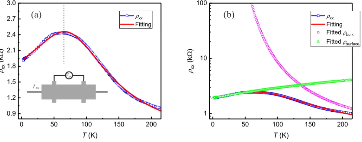
Fig. S1 shows the temperature dependence of the device discussed in the main part of the text. With decreasing temperature, the resistivity of the device increases down to ∼65 K, characteristic for semiconductor-like, bulk dominated conduction, and decreases below∼65 K, typical for metallic-like, surface dominated conduction.
Vxx Ixx
(a) (b)
FIG. S1. R-T relation of the device. (a) The experimental data (blue squares) and corresponding fit (red line). The dashed line approximately separates the bulk and surface conduction dominated regions. (b) The same graph as in (a) in log scale and together with the fitted (see text) bulk (purple) and surface (green) contributions. The inset in (a) shows the measurement configuration.
Useful information, such as carrier density n and activation energy Ea can be extracted from the graph. Following a recent paper1, the surface and the bulk of the topological insulator contribute to the conduction independently, equivalent to resistors connected in parallel. The resistivity of each surface (ρs) can be modeled as metallic like, ρs = ρs,0 + A·T, where ρs,0 and A are constants. The bulk resistivity ρb is thermally activated for temperatures beyond the variable range hopping regime: ρb = ρb,0 ·exp(Ea/kBT), where ρb,0 is a constant, Ea is half the energy gap ∆, andkB is the Boltzmann constant. Thus the total resistivity isρ= (2·ρ−1s +ρ−1b )−1. Here we assume, for simplicity, that the two surfaces are equivalent, having the same carrier density ns and mobility µs. The corresponding fit is shown in Fig. S1a, where we obtained remarkable good agreement. In addition, the fitting also yields ρs = 3801 + 20.5·T, and ρb = 234·exp(31 meV/kBT) and thus the effective energy gap ∆0 = 62 meV. Compared to the nominal energy gap ∆≈300 meV2, the effective gap is 5-times smaller. This is consistent with previous reports3 and a consequence of the coexisting electron and hole puddles which stem from the large potential fluctuations in BSTS.
At sufficiently low temperature (e.g., 1.5 K), the conduction is almost entirely dominated by Dirac surface states, also verified in Ref.4. However, at higher temperatures, bulk carriers are activated and contribute to transport. AtT = 58 K, using the results from the fit above, and by assuming a typical, temperature independent value of µb = 200 cm2/Vs, we obtain nb = 2.7·1011cm−2. The same way, the carrier density at zero gate voltage on each surface isns= 6.3·1011cm−2, using µb = 2000 cm2/Vs. Thus the delocalized bulk carrier density is comparable to that in the surface states.
The bulk carrier density at 58 K, nb, can also be estimated from the constant DOS back- ground Db(T). ARPES measurements show that pristine BSTS is slightly p-type doped.2 Thus, the bulk hole concentrationnb =R0
−∞Db(T = 58 K)(1−f(E−µ))dE, wheref(E−µ) is the Fermi-Dirac function. Db(T = 58 K) = 17.4·1035m−2J−1, can be read from Fig. 3d in the main text. Here, µis slightly below the Dirac point, µ≈ −25 meV.2 With these values one obtains nb = 7·1011cm−2, which is of the same order and comparable to the estimate given above.
-3 -2 -1 0 1 2 3 4.60
4.62 4.64 4.66
DVtg 20 K
C (pF)
Vtg-VCNP (V)
C-V d2C/dV2tg
-1 0 1
d2 C/dV2 tg (x10-13 F2 /V2 )
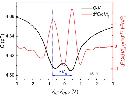
FIG. S2. C-V trace at 20 K and 14 T, and the corresponding second derivative d2C/dVtg2, used to determine ∆Vtg.
II. DETERMINING ∆Vtg
Here we show how ∆Vtg in Fig. 2 and Fig. 3 is determined. As example we use the experimental data taken at 20 K and 14 T, shown in Fig. S2. To enhance the visibility of the minima and to suppress effects of the background we calculate the second derivative of the trace. This results in two pronounced peaks at the position of the minima. The distance between the 2 peaks gives ∆Vtg. This procedure is particularly useful at elevated temperatures where it is more difficult to determine the minimum position accurately from the original capacitance trace.
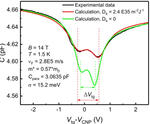
III. FAILURE OF FITTING C-V TRACE AT 14 T WITHOUT BACKGROUND DOS
In Fig. S3 we compare the capacitance measured at B = 14 T and T = 1.5 K to fits with and without using a constant background density. The fits without background density fail to describe the data, especially the voltage difference between the capacitance minima which correspond to the Landau gaps. The distance between calculated, adjacent Landau gaps is
-2 -1 0 1 2 4.56
4.58 4.60 4.62 4.64 4.66
∆Vtg
C (pF)
V
tg-V
CNP(V)
Experimental data
Calculation, Db = 2.4 E35 m-2J-1 Calculation, Db = 0
B = 14 T T = 1.5 K nF = 2.8E5 m/s m* = 0.57*m0 Cpara = 3.0635 pF s = 15.2 meV
FIG. S3. Comparison of fits to the experimental data at 1.5 K and 14 T, with and without finite Db = 2.4·1035 m−2J−1, while the other paramters are kept the same: Fermi velocity νF = 2.8·105 m/s, effective mass m∗ = 0.57m0, Gaussian energy broadening σ = 15.2 meV, and parasitic capacitance Cpara= 3.0635 pF.
always smaller (marked by ∆Vtg in Fig. S3) than observed in experiment if Db is set to 0, no matter how the other parameters are chosen. This discrepancy becomes much larger at higher temperatures.
IV. ESTIMATING THE FILLING RATE FROM HALL MEASUREMENTS.
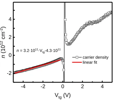
The filling rate dn/dVtg extracted from the position of the Landau gaps on the gate voltage scale in the main text (Fig. 2(a) and Fig. 3(a)) is smaller than C0/e, expected from the insulator capacitance C0. Fig. S4 shows that the reduced filling rate is also measured by the classical Hall slope.
The Hall data were taken at 1.5 K by sweeping the top gate voltage (Vtg) at fixed B, as well as by sweeping B at fixed Vtg. The device shows at such low temperature surface dominated conduction, which takes place in top and bottom surface. From Fig. 1(c) in the
- 4 - 2 0 2 4 - 2
024
c a r r i e r d e n s i t y l i n e a r f i t
n (1012 cm-2 ) V t g ( V )
n = 3 . 2 · 1 0 1 1 · V t g- 4 . 3 · 1 0 1 1
FIG. S4. Estimate of the total carrier densityp using the Hall slope givingp= (edρdBxy)−1 for low magnetic field data. Here the electron density is defined positive, the hole density negative.
main text, we see that at zero gate voltage, both top and bottom surfaces are slightly p- doped. By grounding the back gate and sweepingVtg from 5 to -5 V, one changes the carrier type in the top surface. ForVtg <0 in Fig. S4,p-type conduction prevails in top and bottom surfaces. The total carrier density and the total filling rate in this regime can be simply obtained from the one carrier Drude model. The filling rate, i.e., the change of total density with gate voltage, is given by the slope of the red line in Fig. S4. The corresponding filling rate is 3.2·1011 cm−2V−1. This is consistent with the filling rate displayed by the QHE data in the main text (4·1011cm−2V−1, using ∆Vtg = 0.84 V from Fig. 3(c)). Similar conclusions can be found in4.
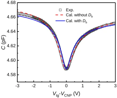
V. COMPARING FITTING OF C-V AT B = 0 T AND T = 1.5 K WITH AND WITHOUT BACKGROUND DOS
The B = 0 capacitance trace in Fig. 1(d) of the main text we fitted without using a background DOSDb. While theB = 0 data can be well fitted usingDb= 0, the capacitance data in quantizing magnetic field can not. In Fig. S5 we show that the data of Fig. 1(d)
- 3 - 2 - 1 0 1 2 3 4 . 5 8
4 . 6 0 4 . 6 2 4 . 6 4 4 . 6 6 4 . 6 8
C (pF) V t g - V C N P ( V )
E x p .
C a l . w i t h o u t D b
C a l . w i t h D b
FIG. S5. Fitting the data of Fig. 1(d) with and without Db atB = 0 T and T = 1.5 K. The red dashed line is the same as the one shown in Fig. 1(d), with fitting parameters vF = 3.2·105m/s, m∗ = 0.47m0, σ = 29.4 meV, parasitic capacitance 3.073 pF, and Db = 0. The blue trace, in contrast, was obtained using the same Db = 2.4·1035m−2J−1 extracted at the same T from the 14 T data. The other fit parameters are thenvF = 2.8·105m/s, m∗ = 0.57m0,σ = 15.2 meV, and parasitic capacitance 3.065 pF.
can be likewise fitted with a finite DOS Db. As a result, the energy broadening becomes significantly smaller, but the important parameters like Fermi velocityvF and effective mass m∗ stay within 20% the same.
VI. A TEMPERATURE-DEPENDENT DOS MODEL
Consider the (normalised) model DOS D˜b(E, µ, T) =
tanhh a+
1 + E−µbT 2 cT2i R E0 tanhh
a+
1 + EbT0−µ2
cT2i, (6)
Eq. (6) extends the T-independent minimal model employed in the manuscript, and takes into account the Coulomb gap T-dependence which arises from its progressive filling by thermal excitations once T 6= 05–10. It does it so as to agree with the universal behavior
obtained by Mogilyanskii and Raikh6 at low T and low energy, with the addition of a constant E = µ offset fixed by a 1. The parameters b, c set the gap shape. Within our phenomenological approach, Eq. (6) does not yield any discernible improvement in the fit of the experimental data.
1 S. Cai, J. Guo, V. A. Sidorov, Y. Zhou, H. Wang, G. Lin, X. Li, Y. Li, K. Yang, A. Li, Q. Wu, J. Hu, S. K. Kushwaha, R. J. Cava, and L. Sun, npj Quant. Mater. 3, 62 (2018).
2 T. Arakane, T. Sato, S. Souma, K. Kosaka, K. Nakayama, M. Komatsu, T. Takahashi, Z. Ren, K. Segawa, and Y. Ando, Nat. Commun. 3, 636 (2012).
3 B. Skinner, T. Chen, and B. I. Shklovskii, Phys. Rev. Lett. 109, 176801 (2012).
4 Y. Xu, I. Miotkowski, C. Liu, J. Tian, H. Nam, N. Alidoust, J. Hu, C.-K. Shih, M. Z. Hasan, and Y. P. Chen, Nat. Phys. 10, 956 EP (2014).
5 M. Grunewald, B. Pohlmann, L. Schweitzer, and D. Wurtz, J. Phys. C: Solid State Phys. 15, L1153 (1982).
6 A. A. Mogilyanskii and M. Raikh, J. Exp. Theor. Phys. 68, 1081 (1989).
7 B. Sandow, K. Gloos, R. Rentzsch, A. N. Ionov, and W. Schirmacher, Phys. Rev. Lett. 86, 1845 (2001).
8 A. Vaknin, Z. Ovadyahu, and M. Pollak, Phys. Rev. B 65, 134208 (2002).
9 E. Bardalen, J. Bergli, and Y. M. Galperin, Phys. Rev. B 85, 155206 (2012).
10 Y. Meroz, Y. Oreg, and Y. Imry, EPL105, 37010 (2014).