Ballistic geometric resistance resonances in a single surface of a topological insulator
Hubert Maier 1 , Johannes Ziegler 1 , Ralf Fischer 1 , Dmitriy Kozlov 2,3 , Ze Don Kvon 2,3 , Nikolay Mikhailov 2 , Sergey A. Dvoretsky 2 & Dieter Weiss 1
Transport in topological matter has shown a variety of novel phenomena over the past decade. Although numerous transport studies have been conducted on three-dimensional topological insulators (TIs), study of ballistic motion and thus exploration of potential landscapes on a hundred nanometer scale is for the prevalent TI materials almost impossible due to their low carrier mobility. Therefore, it is unknown whether helical Dirac electrons in TIs, bound to interfaces between topologically distinct materials, can be manipulated on the nanometer scale by local gates or locally etched regions. Here we impose a submicron periodic potential onto a single surface of Dirac electrons in high-mobility strained mercury telluride (HgTe), which is a strong TI. Pronounced geometric resistance resonances constitute the clear-cut observation of a ballistic effect in three-dimensional TIs.
DOI: 10.1038/s41467-017-01684-0 OPEN
1
Institute of Experimental and Applied Physics, University of Regensburg, 93053 Regensburg, Germany.
2A.V. Rzhanov Institute of Semiconductor Physics, 630090 Novosibirsk, Russia.
3Novosibirsk State University, 630090 Novosibirsk, Russia. Correspondence and requests for materials should be addressed to D.W. (email: dieter.weiss@ur.de)
1234567890
T opological insulators that feature conducting surface states while the bulk is insulating are a new class of materials with unique physical properties (see, e.g., refs. 1,2 and references therein). By combining materials with different topo- logical index, e.g., HgTe which has an inverted band structure with HgCdTe (or CdTe) being a conventional semiconductor, helical two-dimensional electron systems (2DES) form at the interface. These states have a linear, Dirac-like electron dispersion E(k) and are protected from direct backscattering by time reversal symmetry 1,2 . The 2DES of surface states encases the (ideally) insulating bulk. The electron spin in theses surface states is helical, i.e., locked to the electron’s k vector and spin-up (↑) and spin-down states (↓) are for systems with time reversal symmetry connected by Kramers degeneracy, E(k, ↑) = E(−k, ↓). Thus, any k-space state is only singly occupied. This means that the connection between carrier density nsand Fermi wave vector k
Fis given by k
F¼ ffiffiffiffiffiffiffiffiffi
4πn
sp and not k
F¼ ffiffiffiffiffiffiffiffiffi 2πn
sp , as in a conventional 2DES. Clear signatures of the unusual spin texture of three- dimensional TIs have first been seen in Bi
1−xSb
xby angle-resolved photoemission spectroscopy 3,4 .
Here we probe ballistic geometric resonances in an antidot lattice, which directly reflect the wave vector of helical Dirac fermions. An antidot lattice consists of a periodic array of holes etched into the surface and constitutes a periodic, repulsive potential for the electrons in the 2DES 5–7 . Pronounced resonances occur in the magnetoresistance when the ratio of cyclotron radius R
c= ħk
F/(eB) (ħ = reduced Planck constant, e = elementary charge, B = magnetic field) and period a of the antidot lattice enables stable orbits around one or a group of antidots 5 , stabilized by the repulsive potential 8 . Similar effects
were predicted and observed in graphene, also a system with Dirac-like dispersion 9 – 11 . The B-field positions at which the resistance peaks appear are a direct measure of k
F. Such reso- nances have been used, e.g., to experimentally proof the concept of composite fermions 12 and the formation of Wigner crystals 13 . The observation of these commensurability effects requires that the electron mean free path ‘
ea, i.e., high electron mobilities.
Hence, strained HgTe which belongs to the class of strong TIs 14,15 is ideal for these experiments as it features very high electron mobilities of order 5 × 10 5 cm 2 (Vs) −1 , corresponding to electron mean free paths of around 5 microns. Experimental verification that strained HgTe is a TI has been provided before by transport 16,17 , capacitance 18 , and photocurrent experiments 19 . In this material, we observe clear-cut geometric resonances reflecting the superimposed lateral periodic potential.
Results
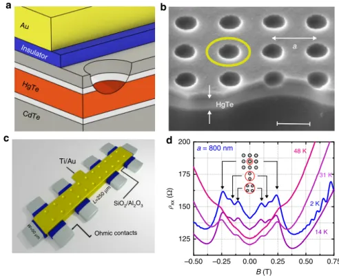
Antidot lattices and characteristic geometric resonances. The present experiments were carried out on strained 80 nm-thick HgTe films, grown by molecular beam epitaxy on CdTe (013).
For details, see ref. 19 . The cross section of the heterostructure is sketched in Fig. 1a. Square antidot lattices with periods a = 408, 600, and 800 nm were defined by electron beam lithography and etched through the cap layers slightly into the HgTe layer. In order to keep the high electron mobility of the surface electrons, we used wet chemical etching to engrave the antidots gently into the material. An electron micrograph of a corresponding antidot lattice is shown in Fig. 1b, illustrating that the antidots get only a few nm into the 80 nm-thick HgTe layer. Transport and
a
Au
HgTe
CdTe Insulator
c d
HgTe
a
a = 800 nm
b
200
175
48 K
31 K
14 K (Ω)xx 2 K
150
125
–0.50 –0.25 0.00 0.25 B (T)
0.50 0.75 Ti/Au
L=250 μm
SiO2/Al2O3
Ohmic contacts
W=50 μm
Fig. 1 Sample layout and antidot resonances. a Layer sequence grown on a virtual CdTe (013) substrate having a 0.3% larger lattice constant than HgTe, causing tensile strain
19. One antidot, slightly etched into the HgTe top layer is sketched. The whole structure is covered by a 30 nm/100 nm-thick SiO
2/Al
2O
3insulator and a metallic top gate consisting of 10 nm/100 nm Ti/Au. b Scanning electron micrograph picture of an antidot lattice with a period of ~400 nm. The sample was tilted by 50° and the scale bar is 300 nm. The 80 nm-thick fi lm of strained HgTe, covered by 20 nm HgCdTe and 40 nm CdTe cap layers stands out by the brighter contrast. c Schematic Hall bar geometry with dimensions. d ρ
xx( B ) of the 800 nm antidot lattice at different temperatures and n
tops1 : 7 ´ 10
15m
2. Peaks in the resistivity correspond to commensurate orbits around 1, 2, and 4 antidots as sketched in the inset. The corresponding arrow positions, characteristic for a strong antidot potential, have been calculated using B
1= ħk
F/(0.5 ea ), B
2= ħk
F/(0.8 ea ), and B
4= ħk
F/(1.14 ea ) with k
F¼ ffiffiffiffiffiffiffiffiffiffiffiffiffi
4 πn
topsp
capacitance experiments were carried out on devices with Hall bar geometry, sketched in Fig. 1c. For transport measurements, carried out at temperatures T between 1.5 and 48 K, we used standard lock-in techniques. Typical traces of resistivity ρ
xx(B), taken at different temperatures, are shown in Fig. 1d and display clear antidot resonances. The positions of the resonances, marked by arrows, correspond to commensurate orbits around one, two, and four antidots occurring at R
c/a = 0.5, 0.8, and 1.14, respec- tively 5 , shown in the inset of Fig. 1d. With increasing tempera- ture, the Shubnikov-de Haas (SdH) oscillations fade away but the antidot resonances are still visible at higher T indicating their semi-classical origin.
The occurrence of clear antidot resonances raises the question about the origin of the repulsive potential as the two-dimensional topological surface states are bound to the interface. Thus, by etching the holes, the boundary between HgTe and vacuum is locally shifted deeper into HgTe but there are no regions devoid of electrons as in a conventional 2DES-based antidot lattice.
Opening the cap layer at the antidot positions and exposing the HgTe surface to ambient conditions most likely increases locally the p-doping thus constituting an electrostatic potential barrier between etched and pristine regions of the HgTe surface.
Etching the array of holes might also introduce a periodic strain pattern, which contributes to the antidot potential in a similar way as ripples affect the band structure in Bi
2Te
320 . Although the
detailed microscopic origin and shape of the antidot potential is unknown yet, its effect on electron transport is clearly visible in Fig. 1d. From the similarity to geometric resonances in GaAs- based 2DES, we conclude that the antidot potential has the diameter of the etched holes and drops precipitously but softly toward the region between the antidots.
Carrier densities and geometric resonances. To establish the connection between Fermi wave vector k
Fand carrier density, we need accurate knowledge of the electron density n
topson the top surface, i.e., the surface locally dented by the antidots. The period of SdH oscillations, taken at high B, or Drude transport data give the total carrier density n
sof the TI system, i.e., the sum of densities on top and bottom surface and, for E
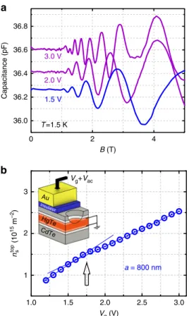
Fin the conduction band, of bulk electrons 17 . Therefore, we resort to measurements of the quantum capacitance which reflects the electronic density of states (DoS) and is sensitive to the top surface only 18 . In capacitance experiments, the top layer dominates, as it screens, to a large extent, the electric field from the gate. The capacitance is measured by adding a small ac voltage to the dc top gate voltage V
gand probing the ac current phase sensitively. Corresponding data are shown in Fig. 2a. The capacitance oscillations of the 800 nm period antidot sample, shown for three different gate voltages, stem from Landau quantization, echoed in the measured DoS. From these measurements, we can extract the carrier density n
topsV
gof the top surface, shown as a function of the gate voltage in Fig. 2b. Here we have used that the spin-degeneracy factor g
s, utilized to extract the carrier density from the period of the capacitance oscillations, is 1, i.e., the Landau levels are not spin degenerate 18 . These data show a striking change of slope at ~1.75 V, marked by an arrow. This reflects a change in the filling rate dn
tops=dV
gand occurs when the Fermi level enters the conduction band 17 . This kink in slope is characteristic for quantities like low-B SdH oscillations 17 , quantum capacitance 18 , or antidot peak position (see below), which all stem from a single topological surface.
Gate voltage and antidot period dependencies. The dc top gate voltage on our devices allows tuning the carrier density and thus the position of the Fermi level E
F. The characteristic evolution of the sheet resistance ρ
□= ρ
□(B = 0) with V
gis shown for three antidot samples and an unpatterned reference sample in Fig. 3a.
The maxima of ρ
xx, located between V
g~ 0.5 and 1 V, reflect the charge neutrality point (CNP), corresponding to an E
Fposition located slightly in the valence band (see band structure in Fig. 3b) 17 . The fact that the CNPs of the patterned samples are shifted to higher gate voltages (clearly for the 408 and 800 nm, only weakly for the 600 nm sample) implies local p-doping.
For gate voltages to the right of the CNP peak, E
Fstarts to move into the gap. The dark blue traces in Fig. 3c show ρ
xx(B) data for V
gbetween 1.2 and 1.7 V at which E
Fis in the gap. The evolution of the fundamental antidot peak position B
1for different V
g, matches perfectly the calculated position at
B
1¼ 2 h ffiffiffiffiffiffiffiffiffiffiffiffi 4πn
topsp
ea ; ð1Þ
marked by arrows. Here for each particular gate voltage n
topshas been derived from the oscillation period of the quantum capacitance. The antidot peaks even withstand moving E
Finto the conduction band (purple curves in Fig. 3c), showing that bulk electrons do not contribute. This happens for V
g> 1.75 V, as deduced from the kink in the capacitance data of Fig. 2b.
Although current also flows through the bottom surface and, for V
g> 1.75 V, through bulk regions, thus contributing to the resistivity, only electrons in the top layer contribute to the geometric transport resonances. At lower bias, however, where E
Fis in the valence band (light blue traces) the antidot peaks quickly a
b
Vg+Vaca = 800 nm
Vg (V) B (T)
Capacitance(pF)
36.8
3.0 V
2.0 V 1.5 V 36.6
36.4
36.2
36.0
3 Au
HgTe CdTe
Insulator
2
1
1.0 1.5 2.0 2.5 3.0
ntop (1015 m–2)s
0 2 4
T=1.5 K
Fig. 2 Capacitance oscillations and density. a Oscillations of the quantum
capacitance with constant Δ (1/ B ) periodicity re fl ect Landau quantization of
Dirac electrons on the top surface. The corresponding carrier density is
given by n
tops¼ e= ð 2 π h Δð 1 =BÞ Þ . b Inset: Capacitance is measured by
superimposing a small ac signal (0.01 V at 50 Hz) onto a dc voltage (which
tunes E
F) and probing the ac current phase sensitively
18. The blue points
show the carrier density of the top surface, n
tops, obtained from the
periodicity of the capacitance oscillations. The arrow marks the gate voltage
at which the slope dn
tops=dV
gchanges. For V
g< 1.75 V the fi lling rate is
1.22 × 10
15m
−2V
−1, for V
g> 1.75 V it is 0.87 × 10
15m
−2V
−1disappear and are hardly visible for V
g= 1 V, i.e., close to the CNP. After we have shown the evolution of the antidot peak position as a function of V
g, i.e., carrier density, we present in Fig. 3d the fundamental peak positions for three different periods at constant carrier density. Also, here the position of the fundamental peak is given by B
1(Eq. 1) and marked by arrows in Fig. 3d. For the 600 and the 800 nm device also the position of the orbits around two ð Þ B
2and four antidots ð Þ B
4are shown. For calculating the resonance position, we have used k
F¼ ffiffiffiffiffiffiffiffiffiffiffiffi
4πn
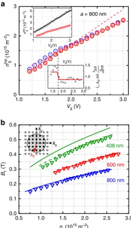
topsp , i.e., the relation between Fermi wave vector and carrier density of a two-dimensional electron gas which is not spin degenerate (see inset of Fig. 4b). The nearly perfect agreement between measured and calculated resonance position is in line with antidot resonances stemming from helical Dirac surface states, which are spin-polarized, as sketched in Fig. 3b, and probe a single topological surface. Figure 4 provides further evidence that the antidot peaks sample the properties of the top surface only. For that, we extract the carrier density from the B-field position at which the fundamental resonance occurs, using n
tops¼ ð eaB
1Þ
2= 16π h
2. The result is shown by the red circles in Fig. 4a. These data points resemble closely n
tops, derived from the quantum capacitance oscillations in Fig. 2b, also shown in Fig. 4a. Most importantly, n
topsV
g, acquired from the antidot resonance position displays a change of slope at about 1.75 V, in analogy to the capacitance data. This is a clear indicator that the antidot signals root in a single topological surface. Therefore, antidot resonances can be used to extract the carrier density of the top surface also at higher temperatures at which quantum oscillations are smeared out. In contrast, the total carrier density,
determined here from the position of the quantum Hall plateaus at high fields and shown in the upper inset of Fig. 4a echoes the total carrier density, i.e., the sum of n
tops, the carrier density of the bottom surface, n
bots, and, for V
g> 1.75 V, n bulk the bulk carrier density. The slope of the total carrier density n
s(V
g), in contrast, is constant and reflects the constant filling rate dn
s/dV
g(upper inset Fig. 4a).
Figure 4b shows the magnetic field positions B
1of the fundamental antidot resonance occurring at 2R
c= a for all three investigated devices. The carrier density n
topsfor each gate voltage has been taken from the quantum capacitance oscillations. The solid lines have been calculated using Eq. (1). The lines describe the data for the 600 and 800 nm antidot lattice perfectly well; in the case of the 408 nm lattice, there is a small deviation of ~10%.
There, the capacitance was measured on a sample area where only a fraction of ~18% was covered with antidots. Therefore, the extracted n
topsis an average value, which is slightly higher than the carrier density in the antidot lattice. By assuming a 20% reduced carrier density in the antidot patterned areas compared to pristine ones, a plausible value for our system, we obtain a perfect match with experiment (green dashed line in Fig. 4b).
Discussion
In the present work, we have imposed a (periodic) potential on the nanometer scale onto a single surface of Dirac electrons and observe clear geometric resonances, which stem from the upper topological surface. This is of central importance for all kinds of (ballistic) manipulation of helical Dirac electrons on the
vb Dss
b d
a c
150 150 300 450 700 600
350
0–1 0
cb Unstructured
1 2
50 100
–0.5 0.0 0.5
60 90
408 nm
600 nm xx (Ω)xx (Ω)
800 nm 800 nm
Vg (V)
B (T)
–0.5 0.0 0.5
B (T) 800 nm
600 nm 408 nm
(Ω)
Fig. 3 Magnetoresistance of three antidot superlattices. a Sheet resistance ρ
□vs. V
gof an unpatterned reference sample and three antidot lattices with
a = 408, 600, and 800 nm. The dashed line marks the CNP of the unpatterned sample. b Schematic band structure showing the conduction band (cb), the
valence band (vb), and the Dirac surface states (Dss). c ρ
xx( B ) traces taken from the 800 nm antidot lattice at gate voltages V
g= 0.8, 1, 1.2, 1.4, 1.7, 2, 2.4 V
(from top to bottom). The dashed arrow points in the direction of increasing E
F. The fundamental antidot peaks, corresponding to a cyclotron orbit fi tting
around one antidot (inset) have been calculated from n
topsand are marked by arrows. d Low fi eld ρ
xx( B ) traces showing antidot resonance for the three
investigated periods. n
topswas adjusted to ~2.2 × 10
15m
−2for all traces via V
g. The arrows mark calculated values of the fi eld B
1, and for the 600 and
800 nm sample also B
2and B
4. The lower zero fi eld resistance of the 600 nm sample we ascribe to a longer exposure to 80 °C during insulator deposition
nanoscale. The antidot resonances probed here reveal the Fermi wave vector, being consistent with Dirac surface states, which are singly occupied in k-space.
Methods
Device fabrication. The first step in device fabrication is defining the antidots by electron beam lithography and etching the antidot slightly into the HgTe layer by using a wet chemical etching solution containing 0.1 ml bromine, 100 ml ethylene glycol, and 25 ml distilled water. To ensure reproducible etching rates, the solution is cooled to 0 °C. The etched antidots have a diameter between 170 and 190 nm.
After etching the antidots, we defined and etched a Hall bar by optical lithography and wet chemical etching. By etching the Hall bar after nanostructuring, we remove differently deep etched antidots, which occur along the perimeter of the patterned area between the potential probes so that they do not matter in transport experi- ments. As gate insulator, we deposited 30 nm SiO
2using a plasma-enhanced chemical vapor deposition process followed by atomic layer depositing of 100 nm Al
2O
3; both processes were carried out at 80 °C. In a final patterning step, we
defined a titanium/gold (10 nm/100 nm) gate by thermal evaporation. Finally, ohmic contacts to HgTe where formed by indium soldering.
Capacitance measurements. The capacitance measurements where performed at 1.5 K in a
4He cryostat with magnetic fields up to 14 T. For these measurements, we used an Andeen – Hagerling (AH) 2700A capacitance bridge with a modulation amplitude of 0.01 V at 50 Hz.
Magnetotransport measurements. We used conventional Hall bar geometries having a width of 50 µm and a length of 650 µm with four potential probes of width 5 µm on each side, separated by either 100 or 250 µm. The resistivity ρ
xx(B) was extracted from areas of size 100 µ m × 50 µ m or 250 µ m × 50 µ m, respectively.
Standard four-terminal measurements were carried out at 1.5 K, unless specified otherwise, using digital lock-in amplifiers (Signal Recovery 7265/EG&G Instru- ments 7260) at a frequency of 13 Hz. A Yokogawa 7651 DC source was used to apply the gate voltage.
Data availability. The data supporting the fi ndings of this study are available within the paper and from the corresponding author on request.
Received: 30 June 2017 Accepted: 9 October 2017
References
1. Hasan, M. Z. & Kane, C. L. Colloquium: topological insulators. Rev. Mod. Phys.
82, 3045–3067 (2010).
2. Ando, Y. Topological insulator materials. J. Phys. Soc. Jpn 82, 102001 (2013).
3. Hsieh, D. et al. Observation of unconventional quantum spin textures in topological insulators. Science 323, 919–922 (2009).
4. Nishide, A. et al. Direct mapping of the spin-filtered surface bands of a three- dimensional quantum spin Hall insulator. Phys. Rev. B 81, 041309 (2010).
5. Weiss, D. et al. Electron pinball and commensurate orbits in a periodic array of scatterers. Phys. Rev. Lett. 66, 2790 – 2793 (1991).
6. Ensslin, K. & Petroff, P. M. Magnetotransport through an antidot lattice in GaAs-Al
xGa
1−xAs heterostructures. Phys. Rev. B 41, 12307 – 12310 (1990).
7. Lorke, A., Kotthaus, J. P. & Ploog, K. Magnetotransport in two-dimensional lateral superlattices. Phys. Rev. B 44, 3447–3450 (1991).
8. Fleischmann, R., Geisel, T. & Ketzmerick, R. Magnetoresistance due to chaos and nonlinear resonances in lateral surface superlattices. Phys. Rev. Lett. 68, 1367–1370 (1992).
9. Pedersen, T. G. et al. Graphene antidot lattices: designed defects and spin qubits. Phys. Rev. Lett. 100, 136804 (2008).
10. Shen, T. et al. Magnetoconductance oscillations in graphene antidot arrays.
Appl. Phys. Lett. 93, 122102 (2008).
11. Sandner, A. et al. Ballistic transport in graphene antidot lattices. Nano Lett. 15, 8402 – 8406 (2015).
12. Kang, W., Stormer, H. L., Pfeiffer, L. N., Baldwin, K. W. & West, K. W. How real are composite fermions? Phys. Rev. Lett. 71, 3850 – 3853 (1993).
13. Deng, H. et al. Commensurability oscillations of composite fermions induced by the periodic potential of a wigner crystal. Phys. Rev. Lett. 117, 096601 (2016).
14. Fu, L. & Kane, C. L. Topological insulators with inversion symmetry. Phys. Rev.
B 76, 045302 (2007).
15. Wu, S.-C., Yan, B. & Felser, C. Ab initio study of topological surface states of strained HgTe. Europhys. Lett. 107, 57006 (2014).
16. Brüne, C. et al. Quantum hall effect from the topological surface states of strained bulk HgTe. Phys. Rev. Lett. 106, 126803 (2011).
17. Kozlov, D. A. et al. Transport properties of a 3D topological insulator based on a strained high-mobility HgTe fi lm. Phys. Rev. Lett. 112, 196801 (2014).
18. Kozlov, D. A. et al. Probing quantum capacitance in a 3D topological insulator.
Phys. Rev. Lett. 116, 166802 (2016).
19. Dantscher, K. M. et al. Cyclotron-resonance-assisted photocurrents in surface states of a three-dimensional topological insulator based on a strained high- mobility HgTe film. Phys. Rev. B 92, 165314 (2015).
20. Okada, Y. et al. Ripple-modulated electronic structure of a 3D topological insulator. Nat. Commun. 3, 1158 (2012).
Acknowledgements
We thank Klaus Richter for valuable discussions and acknowledge funding by the German Science Foundation (DFG) via SPP 1666 and by the Elite Network of Bavaria (K-NW-2013-258). D.K. acknowledges support from RF President Grant No. MK- 3603.2017.2, and N.M. from RFBR Grant No. 15-52-16008.
a
b
kx ky
kF
0.5 1.0 1.5 2.0 2.5 3.0
0.0 0.1 0.2 0.3 0.4 0.5 0.6
408 nm
600 nm 800 nm B1 (T)
ns (1015 m–2)
1.0 1.5 2.0 2.5
s
0 3.0 1 2 3
Vg (V)
1 2 3
1 2 3 4 5
1.5 2.0 2.5 3.00.5 1.0 1.5
(m–2V–1)dVg dntop Vg(V)
Vg(V)
a = 800 nm
Sntop (1015 m–2) Sntop (1015 m–2)
Fig. 4 Geometric antidot resonances. a Carrier density n
topsextracted from
the position of the fundamental antidot peak. n
topsV
gdisplays a distinct
change of slope at ~1.75 V highlighted in the lower inset, which shows
dn
tops=dV
gvs. V
g. Gray points in the inset are obtained by taking the average
slope between three succeeding points, the red line is the best fi t (dashed
lines in main graph) of the slope above and below V
g~ 1.75 V. The fi lling
rate dn
tops=dV
gin the gap is 1.21 × 10
15m
−2V
−1and 0.84 × 10
15m
−2V
−1for
E
Fin the conduction band. These values are very close to the ones obtained
from capacitance oscillations, displayed as blue circles for comparison. The
upper inset shows the total carrier density n
sextracted from the magnetic
fi eld position of the quantum Hall plateaus compared to the red data points
of the main graph (same units as main graph). b B - fi eld position of the
fundamental antidot resonance of the three different antidot lattices
compared to the expected position (solid lines) using Eq. (1). The dashed
line for the 408 nm sample shows the calculated B
1( n
s) trace with corrected
carrier density (see text). The inset shows a schematic of k-space in which
the occupied states (black dots) are not spin degenerate
Author contributions
D.W. conceived the experiments. N.M. and S.A.D. grew the material. H.M. prepared the sample, performed the measurements, and analyzed the data with contributions from D.K., Z.D.K., J.Z., R.F., and D.W. All authors contributed to analyzing and interpreting the data. H.M. and D.W. wrote the manuscript.
Additional information
Competing interests:
The authors declare no competing
financial interests.Reprints and permission
information is available online at
http://npg.nature.com/reprintsandpermissions/
Publisher's note:
Springer Nature remains neutral with regard to jurisdictional claims in published maps and institutional affiliations.
Open Access
This article is licensed under a Creative Commons Attribution 4.0 International License, which permits use, sharing, adaptation, distribution and reproduction in any medium or format, as long as you give appropriate credit to the original author(s) and the source, provide a link to the Creative Commons license, and indicate if changes were made. The images or other third party material in this article are included in the article’s Creative Commons license, unless indicated otherwise in a credit line to the material. If material is not included in the article’s Creative Commons license and your intended use is not permitted by statutory regulation or exceeds the permitted use, you will need to obtain permission directly from the copyright holder. To view a copy of this license, visit
http://creativecommons.org/licenses/by/4.0/.