Probing Quantum Capacitance in a 3D Topological Insulator
D. A. Kozlov,1,2,3 D. Bauer,3 J. Ziegler,3 R. Fischer,3 M. L. Savchenko,1,2 Z. D. Kvon,1,2 N. N. Mikhailov,1 S. A. Dvoretsky,1 and D. Weiss3
1A. V. Rzhanov Institute of Semiconductor Physics, Novosibirsk 630090, Russia
2Novosibirsk State University, Novosibirsk 630090, Russia
3Experimental and Applied Physics, University of Regensburg, D-93040 Regensburg, Germany (Received 3 November 2015; revised manuscript received 7 December 2015; published 22 April 2016)
We measure the quantum capacitance and probe thus directly the electronic density of states of the high mobility, Dirac type two-dimensional electron system, which forms on the surface of strained HgTe. Here we show that observed magnetocapacitance oscillations probe—in contrast to magnetotransport— primarily the top surface. Capacitance measurements constitute thus a powerful tool to probe only one topological surface and to reconstruct its Landau level spectrum for different positions of the Fermi energy.
DOI:10.1103/PhysRevLett.116.166802
Three-dimensional topological insulators (3D TI) represent a new class of materials with insulating bulk and conducting two-dimensional surface states [1–4].
The properties of these surface states are of particular interest as they have a spin degenerate, linear Dirac-like dispersion with spins locked to their electrons’ kvectors [4,5]. Strained HgTe, examined here, constitutes a 3D TI with high electron mobilities allowing the observation of Landau quantization and quantum Hall steps down to low magnetic fields[6,7]. While unstrained HgTe is a zero gap semiconductor with inverted band structure[8,9], the degenerate Γ8 states split and a gap opens at the Fermi energyEF if strained. This system is a strong topological insulator [10], explored by transport [6,7,11], angle- resolved photoemission spectroscopy[12], photoconduc- tivity, and magneto-optical experiments[13–16]; also, the proximity effect has been investigated [17]. Since these two-dimensional electron states (2DES) have high elec- tron mobilities of several 105 cm2=V s, pronounced Shubnikov–de Haas (SdH) oscillations of the resistivity and quantized Hall plateaus commence in quantizing magnetic fields [6,7,11], stemming from both top and bottom 2DES. The oscillations stem from Landau quantization which strongly modifies the density of states (DOS). Capacitance spectroscopy allows us to directly probe the thermodynamic DOS dn=dμ (n¼carrier density, μ¼electrochemical potential), denoted asD, of a 3D TI. The total capacitance measured between a metallic top gate and a 2DES depends, besides the geometric capacitance, on the quantum capacitance e2D, connected in series and reflecting the finite density of states D of the 2DES [18–22]; e is the elementary charge. Below, the quantum capacitance of the top surface is denoted ase2Dt, the one of the bottom layer bye2Db. We show that capacitance measures, in contrast to trans- port, the properties of a single Dirac cone in a 3D TI.
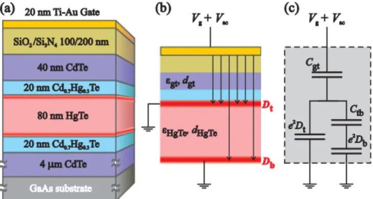
The experiments are carried out on strained 80 nm thick HgTe films, grown by molecular beam epitaxy on
CdTe (013). For details, see [16]. The Dirac surface electrons have high electron mobilities of order 4×105cm2=V s. The cross section of the structure is sketched in Fig. 1(a). For transport and capacitance measurements, carried out on one and the same device, the films were patterned into Hall bars with metallic top gates. Several devices from the same wafer have been studied. The measurements were performed at temperature T¼1.5K and in magnetic fields B up to 13 T. For magnetotransport measurements the standard lock-in tech- nique has been applied. For the capacitance measurements we superimpose the dc biasVgwith a small ac voltage and measure the ac current flowing across our device phase sensitively. The absence of both leakage currents and
FIG. 1. (a) Cross section of the heterostructures studied. The Dirac surface states (red) enclose the strained HgTe layer.
(b) Schematics of the “three plate capacitor” formed by the metallic top gate and top and bottom layer (red) with density of statesDtandDb, respectively. The electric field (black arrows) is partially screened by the top surface layer. (c) Corresponding equivalent circuit with the quantum capacitances Ae2Dt and Ae2Dbin series with the respective geometrical capacitances. The equivalent circuit is the one introduced in[22], but extended by the quantum capacitance of the bottom surface,Ae2Db. A similar equivalent circuit was recently introduced in[23].
resistive effects were controlled by the real part of the measured ac current.
When the Fermi level (electrochemical potential) is located in the bulk gap the system can be viewed as a
“three-plate”capacitor where the top and bottom surfaces form the two lower plates [see Fig. 1(b) and the corre- sponding equivalent circuit in Fig.1(c)]. From this equiv- alent circuit it follows that, as long asDbdoes not vanish, the measured total capacitance is more sensitive to changes ofDt than ofDb; the explicit connection betweenDt,Db and total capacitance C is given in the Supplemental Material [24]. The ratio of ðdC=dDtÞ=ðdC=dDbÞ ¼ ðADbe2þCtbÞ2=C2tbis significantly larger than unity since ADbe2þCtbis (atB¼0) at least a factor of 2 larger than Ctb. Here, Ctb is the geometric capacitance Ctb¼ εHgTeε0A=dHgTe between top and bottom surface, with εHgTe≈21, the dielectric constant of HgTe[25], dHgTe is the thickness of the HgTe film,Ais the gated TI area, andε0
the dielectric constant of vacuum. Therefore, the measured capacitance reflects primarily the top surface’s DOS,Dt. In the limit Ctb →0or e2Db→0 the total capacitance Cis given by the expression usually used for conventional 2DES:1=C¼1=Cgtþ1=Ae2Dwith the geometric capaci- tanceCgt ¼εgtε0A=dgt, whereεgt is the dielectric constant of the layers between gate and top 2DES, dgt is the corresponding thickness [20,21]. Note that Cgt ≪e2Dt; therefore, variations of the DOS cause only small changes ofC. First quantum capacitance measurements have been reported for Bi2Se3, but the experiments were carried out at high frequencies at which resistive effects prevail [26].
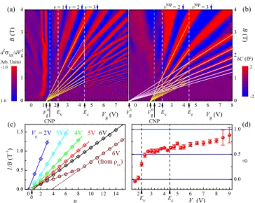
Typicalρxxandρxytraces as function ofVgare shown in Fig. 2(a). ρxx displays a maximum near Vg¼1.5V, whereas ρxy changes sign; this occurs in the immediate vicinity of the charge neutrality point (CNP) [7]. The corresponding capacitance CðVgÞ at B¼0 in Fig. 2(b) exhibits a broad minimum between 2.2 and 4.5 V and echoes the reduced DOS Dt and Db of the Dirac 2DES when the Fermi energy EF is in the gap of HgTe. For Vg>4.5V, EF moves into the conduction band where surface electrons coexist with the bulk ones. There, the capacitance (and thus the DOS) is increased and grows only weakly with increasing Vg. The weak increase of C with jVgj, is ascribed to an increase ofCgtat higherjVgjsince the carriers’wave function is“pressed”towards the interface, an effect neglected in our description[20,21]. ReducingVg below 2.2 V shiftsEF below the valence band edge so that surface electrons and bulk holes coexist. A strong positive magnetoresistance, a nonlinear Hall voltage, and a strong temperature dependence of ρxx provide independent con- firmation thatEFis in the valence band[7]. Because of the valley degeneracy of holes in HgTe and the higher effective mass, the DOS, and therefore the measured capacitanceC is highest in the valence band.
For B well below 1 T both CðVgÞ and ρxxðVgÞ start to oscillate and herald the formation of Landau levels (LLs).
The CðVgÞ trace oscillates around the B¼0 capacitance, shown forB¼2T in Fig.2(b). These oscillations, reflect- ing DOS oscillations, are more pronounced on the electron side (right of the CNP). This electron-hole asymmetry stems mainly from the larger hole mass, leading to reduced LL separation for the holes. At higher fields Hall conductivity σxyand resistivityρxy(not shown) become fully quantized.
σxyðVgÞ, shown for B¼4, 7, and 10 T in Fig.2(c), shows quantized steps of heighte2=h (h¼Planck’s constant), as expected for spin-polarized 2DES.
Transport and capacitance data in the whole Vg and B space are presented in Figs.2(d)and2(e)as 2D color maps (see Supplemental Material [24] for additional informa- tion). We start with discussingσxx¼ρxx=ðρ2xxþρ2xyÞdata in Fig. 2(d)first. The sequence of σxx extrema is almost symmetrical to the CNP where electron and hole densities match. At fixedBthe distance ΔVg between neighboring σxxminima corresponds to a change of densityΔn¼eB=h from which we calculate the filling ratedn=dVg ¼αtotal¼ 7.6×1010 cm−2=V at 10 T. The filling rateαtotaldescribes the change of the total carrier density n with Vg. Comparison of electron densities extracted in the classical Drude regime with densities taken from the periodicity of FIG. 2. (a) TypicalρxxðVgÞandρxyðVgÞtraces measured atB¼ 0and B¼4T.ρxx displays a maximum and ρxy changes sign around the CNP. (b) Capacitance measured at B¼0 and B¼2T. The pronounced minimum of the B¼0 capacitance corresponds to the reduced DOS whenEFis in the gap. Hence, the band edges are atEv≈2.2V andEc≈4.4V. The quantum oscillations of the capacitance reflect the oscillations of the DOS.
(c) Hall conductivityσxyðVgÞmeasured forB¼4T (black), 7 T (red), and 10 T (green). Quantized steps occur on the hole and electron side. (d) 2D color map of normalizedσxxðVg; BÞ data.
The red color stands forσxxmaxima while the blue color displays minima. From the distance between theσxxminima we extract a filling rate ofαtotal¼7.6×1010 cm−2=V (see text). This allows constructing a LL fan chart (dashed yellow lines) which describes the low filling factors ν well. (e) 2D color map of δCðBÞ ¼ CðBÞ−Cð0Þas function ofBandVg. As in (d), the blue color displays gaps between LLs (DOS minima). The LL fan chart is the same as in (d). CNP,Ec, andEvare marked on thexaxis.
SdH oscillations have shown thatσxxoscillations at highB reflect the total carrier density in the TI, i.e., charge carrier densities in the bulk plus in top and bottom surfaces [7].
αtotal is directly proportional to C=A¼edn=dVg and corresponds toC=A¼eαtotal ¼1.22×10⁻⁴F=m2, a value close to the calculated capacitance Ccalcgt =A¼1.45× 10⁻⁴ F=m2 using thickness and dielectric constant of the layers [see Figs. 1(a) and 1(c) and the Supplemental Material [24] ]. Using this αtotal, the Landau level fan, i.e., the calculated positions of theσxxminima as a function ofVgandB, fits the data for low filling factorsνquite well.
For ν larger than 2 on the electron side the fan chart significantly deviates from experiment and is discussed using higher resolution data below. On the hole side where SdH oscillations stem from bulk holes, fan chart and experimental data match almost over the whole ðVg; BÞ range. We now turn to the magnetocapacitance dataδC¼ CðVg; BÞ−CðVg; B¼0Þshown in Fig.2(e). The data are compared to the same fan chart derived from transport. On the electron side, measuredδC minima display a reduced slope compared to the transport fan chart, pointing to a reduced filling rate. This is a first indication that capaci- tance does not reflect the total carrier density in the system but predominantly the one of the top 2DES only. On the hole side the LL fan chart fits the data quite well but in contrast to transport, LL features are less well resolved there. This asymmetry is related with the different effective masses; the enhanced visibility in transport is due to that fact that SdH oscillations depend onD2while the capaci- tance depends onD only.
Previous transport experiments have shown that the periodicity of the SdH oscillations is changed at small B, corresponding to a reduced carrier density[7]. While at high fields the SdH oscillations reflect the total carrier density they echo the carrier density of the top surface at sufficiently low B. This is due to the fact that SdH oscillations get, with increasing B, first resolved in the layer with the higher density and mobility, i.e., higher partial conductivity and lower LL level broadening[7].
We now compare data taken atBup to 4 T, displayed in Figs. 3(a) and 3(b), which show marked differences between transport and capacitance. We start with discus- sing the capacitance data first. The capacitance [Fig.3(b)]
shows uniform oscillations of δCwith maxima positions, corresponding to different LLs, which are perfectly fitted by two fan charts featuring a distinct crossover at about Vg¼4.4V. The crossover stems from EF entering the conduction band causing a reduced filling rate for Vg>4.4V. From the distance ofδCminima (or maxima) at constant B we can extract the filling rate αgaptop in the gap (2.2V< Vg<4.4V) and for EF in the conduction band, αbulktop . From Fig. 3(b) we obtain αgaptop ¼5.25× 1010 cm−2=V andαbulktop ¼3.3×1010 cm−2=V. This means that in the gap αgaptop=αtotal¼70% of the total filling rate apply to the top surface while the remaining 30% can be
ascribed to the bottom surface. The reducedαbulktop for EF in the conduction band is0.44αtotaland hence the remaining filling rate of 56% is shared between bulk and back surface filling. We note that we obtain reasonable values for the filling rates only when we assume spin-resolved LLs. Since there is no signature of spin splitting down to 0.6 T, where the oscillations fade, the quantum oscil- lations stem from nondegenerate LLs, proving the topo- logical nature of the charge carriers. The extrapolation of the two fan charts towardsB→0defines two points on the Vgaxis, denoted asV0g ¼1.25V andV1g ¼−0.5 V. These points correspond to vanishing electron densityntopon the top surface in case the respective filling ratesαgaptop andαbulktop
would stay constant over the entireVgrange. This is not the case as αbulktop ¼constant only applies for EF in the con- duction band and αgaptop ¼constant for EF in the gap.
Moving EF into the valence band greatly reduces this filling rate. Therefore,V0gandV1gcorrespond only to virtual zeros of the electron density while the real one is much deeper in the valence band.
We now turn to the transport data in Fig.3(a). To get a better resolution of the low field SdH oscillations we plot d2σxx=dV2g in Fig.3(a); as before, red regions indicateσxx
FIG. 3. (a) 2D color map ofd2σxx=dV2g between 0 and 4 T.
The red color indicatesσxxmaxima, the blue color LL’s gaps. The yellow fan chart, here marking in contrast to Fig.2LLs, is the one taken from (b). Already in the gap the LLs branch out, marked by the dotted window and forVg>4.5V the data can no longer be described by a simple fan; the pattern is entangled in a complicated way, suggesting that electrons of top and bottom surface and the bulk contribute. (b) Capacitance data correspond- ing to (a) show a quite regular Landau fan chart. The experimental data can be fitted by two fan charts originating atV0gandV1g. The different slope of the two fan charts resembles the different filling ratesαgaptopandαbulktop (see text). (c)δCminima forVg¼2;…;6V andρxxminima forVg¼6V positions on a1=Bscale. (d) Phase of theδCoscillations as a function ofVg. The gap is marked by vertical dashed lines.
maxima. While the same LL fan fits the lowB-field data (a close-up of the data is shown and discussed in the Supplemental Material [24]) striking deviations occur at higherB. (i) Transport data forEFin the gap show splitting of the LLs and for Vg >4.4V; i.e., for EF in the conduction band, a very complex structure with crossing LLs evolves. (ii) The filling factors given on top of Fig.3(b) are the ones of the electrons in the top surface only, while the filling factors given in Fig.3(a)are the ones of the total carrier density. (iii) Extra splitting of the maxima occurs also in the gap region, most pronounced in the marked region. We thus conclude that in transport the three available transport channels (top, bottom surface electrons, bulk electrons) contribute to the signal and lead to a complicated pattern of the quantum oscillations as a function of B andVg, involving transport via side facets.
The oscillations ofδC, in contrast, stem preferentially from the top surface and allow probing the LL spectrum of a single Dirac surface. Corrections to that likely occur at highBandVg; a level splitting at (Vg≈7V, B≈3T) in Fig. 3(b)suggests that signals from bulk or back surface can affect also δC at higher B, although to a far lesser degree when compared to transport.
The fact that the data are best described by spin-resolved LL degeneracy indicates the surface states’ topological nature. The phase of the quantum oscillationsδdefined by ð1=Bmin;nÞ=Δ1=B¼nþδ is another indicator of topologi- cal surface states [27]. Here, Bmin;n is the magnetic field position of the nth oscillation minimum and Δ1=B is the period of the oscillations on the 1=B scale. The phase can be obtained by plotting the integer oscillation indexn vs 1=Bmin;n. This is shown in Fig. 3(c) both for δC (Vg¼2;…;6V) and transport oscillations (for Vg¼6V). While theδCminima lie on straight lines with interceptsδshown in Fig.3(d), the corresponding transport minima display two slopes. At low fields, where the oscillations stem from the top surface only, the phase factor is δ¼0.720.04 showing the same value as extracted from capacitance¼0.70.04, but for high field SdH oscillations, stemming from both layers,δ∼0, as for conventional 2DES. In Fig.3(d)we show the evolution ofδ as a function of Vg. ForEF in the gap δ is close to 0.5 expected for ideal Dirac fermions of a single surface. δ vanishes quickly for EF entering the valence band and gradually for increasing Vg. The latter we ascribe to increasing hybridization of the surface and bulk states deep in the conduction band. Our experiments prove that a finite phase δ which is a direct fingerprint of the Berry phase acquired by electrons in B fields, can only be observed if the oscillations stem from a single topological surface.
In summary, we present measurements of the quantum capacitance of a TI which directly reflects the DOS of Dirac surface states. The magneto-oscillations of the quantum capacitance allow tracing the LL structure of a single Dirac
surface. The complimentary information provided by trans- port and capacitance experiments is promising in getting a better understanding of the electronic structure of TIs, the latter being particularly important for potential applications of this new class of materials.
We acknowledge funding by the Elite Network of Bavaria (K-NW-2013-258), by the German Science Foundation (DFG) via SPP 1666 and by the Volkswagen Foundation. This work was partially supported by RFBR Grants No. 14-02-31631, No. 15-32-20828, and No. 15- 52-16008.
[1] M. Z. Hasan and C. L. Kane, Rev. Mod. Phys. 82, 3045 (2010).
[2] J. E. Moore,Nature (London)464, 194 (2010).
[3] X.-L. Qi and S.-C. Zhang,Rev. Mod. Phys.83, 1057 (2011).
[4] Y. Ando,J. Phys. Soc. Jpn. 82, 102001 (2013).
[5] C. L. Kane and E. J. Mele, Phys. Rev. Lett. 95, 226801 (2005).
[6] C. Brune, C. X. Liu, E. G. Novik, E. M. Hankiewicz, H.
Buhmann, Y. L. Chen, X. L. Qi, Z. X. Shen, S. C. Zhang, and L. W. Molenkamp,Phys. Rev. Lett.106, 126803 (2011).
[7] D. A. Kozlov, Z. D. Kvon, E. B. Olshanetsky, N. N.
Mikhailov, S. A. Dvoretsky, and D. Weiss,Phys. Rev. Lett.
112, 196801 (2014).
[8] S. H. Groves, R. N. Brown, and C. R. Pidgeon,Phys. Rev.
161, 779 (1967).
[9] K. Seeger,Semiconductor Physics, Springer Series in Solid State Sciences Vol. 40 (Springer, Berlin, 1985).
[10] L. Fu and C. L. Kane,Phys. Rev. B76, 045302 (2007).
[11] C. Brune, C. Thienel, M. Stuiber, J. Bottcher, H. Buhmann, E. G. Novik, C.-X. Liu, E. M. Hankiewicz, and L. W.
Molenkamp,Phys. Rev. X4, 041045 (2014).
[12] O. Crauste, Y. Ohtsubo, P. Ballet, P. A. L. Delplace, D.
Carpentier, C. Bouvier, T. Meunier, A. Taleb-Ibrahimi, and L. Levy,arXiv:1307.2008 (2013).
[13] A. M. Shuvaev, G. V. Astakhov, C. Brune, H. Buhmann, L. W. Molenkamp, and A. Pimenov,Semicond. Sci. Tech- nol.27, 124004 (2012).
[14] A. M. Shuvaev, G. V. Astakhov, M. Muhlbauer, C. Brune, H. Buhmann, and L. W. Molenkamp,Appl. Phys. Lett.102, 241902 (2013).
[15] A. M. Shuvaev, G. V. Astakhov, G. Tkachov, C. Brune, H.
Buhmann, L. W. Molenkamp, and A. Pimenov,Phys. Rev. B 87, 121104(R) (2013).
[16] K.-M. Dantscher, D. A. Kozlov, P. Olbrich, C. Zoth, P.
Faltermeier, M. Lindner, G. V. Budkin, S. A. Tarasenko, V. V. Bel’kov, Z. D. Kvon, N. N. Mikhailov, S. A. Dvoretsky, D. Weiss, B. Jenichen, and S. D. Ganichev,Phys. Rev. B92, 165314 (2015).
[17] I. Sochnikov, L. Maier, C. A. Watson, J. R. Kirtley, C.
Gould, G. Tkachov, E. M. Hankiewicz, C. Brune, H.
Buhmann, L. W. Molenkamp, and K. A. Moler, Phys.
Rev. Lett.114, 066801 (2015).
[18] F. Stern,Appl. Phys. Lett.43, 974 (1983).
[19] T. P. Smith, B. B. Goldberg, P. J. Stiles, and M. Heiblum, Phys. Rev. B32, 2696 (1985).
[20] T. P. Smith, W. I. Wang, and P. J. Stiles,Phys. Rev. B34, 2995 (1986).
[21] V. Mosser, D. Weiss, K. v Klitzing, K. Ploog, and G.
Weimann,Solid State Commun. 58, 5 (1986).
[22] S. Luryi,Appl. Phys. Lett.52, 501 (1988).
[23] Y. Baum, J. Bottcher, C. Brune, C. Thienel, L. W. Molen- kamp, A. Stern, and E. M. Hankiewicz,Phys. Rev. B 89, 245136 (2014).
[24] See Supplemental Materials at http://link.aps.org/
supplemental/10.1103/PhysRevLett.116.166802for details.
[25] J. Baars and F. Sorger,Solid State Commun.10, 875 (1972).
[26] F. Xiu, N. Meyer, X. Kou, L. He, M. Lang, Y. Wang, X. Yu, A. V. Fedorov, J. Zou, and K. L. Wang,Sci. Rep. 2, 669 (2012).
[27] A. A. Taskin and Y. Ando, Phys. Rev. B 84, 035301 (2011).