Photogalvanic probing of helical edge channels in two-dimensional HgTe topological insulators
K.-M. Dantscher,1D. A. Kozlov,2,3M. T. Scherr,1S. Gebert,1J. Bärenfänger,1M. V. Durnev,4S. A. Tarasenko,4 V. V. Bel’kov,4N. N. Mikhailov,2S. A. Dvoretsky,2Z. D. Kvon,2,3J. Ziegler,1D. Weiss,1and S. D. Ganichev1
1Terahertz Center, University of Regensburg, 93040 Regensburg, Germany
2A.V. Rzhanov Institute of Semiconductor Physics, Novosibirsk 630090, Russia
3Novosibirsk State University, Novosibirsk 630090, Russia
4Ioffe Institute, 194021 St. Petersburg, Russia (Received 28 December 2016; published 8 May 2017)
We report on the observation of a circular photogalvanic current excited by terahertz laser radiation in helical edge channels of two-dimensional (2D) HgTe topological insulators (TIs). The direction of the photocurrent reverses by switching the radiation polarization from a right-handed to a left-handed one and, for fixed photon helicity, is opposite for the opposite edges. The photocurrent is detected in a wide range of gate voltages.
With decreasing the Fermi level below the conduction band bottom, the current emerges, reaches a maximum, decreases, changes its sign close to the charge neutrality point (CNP), and again rises. Conductance measured over a≈3μm distance at CNP approaches 2e2/ h, the value characteristic for ballistic transport in 2D TIs. The data reveal that the photocurrent is caused by photoionization of helical edge electrons to the conduction band.
We discuss the microscopic model of this phenomenon and compare calculations with experimental data.
DOI:10.1103/PhysRevB.95.201103
The quantum spin Hall (QSH) effect occurs in 2D TIs and rests on the existence of conducting helical edge states while the bulk is insulating [1–4]. In contrast to the quantum Hall effect, the formation of these edge states requires no magnetic field: they stem from the band inversion caused by strong spin-orbit interaction and are topologically protected by time reversal symmetry. Given that the spin-up and spin-down electrons propagate along an edge in opposite directions, i.e., the spin projection is locked to thekvector, the edge channels are helical in nature. The first experimental evidence for the QSH effect was obtained in HgTe quantum wells (QWs) [5] by observing a resistance plateau aroundh/2e2in the longitudinal resistance of a mesoscopic Hall bar. Herehis Planck’s constant andeis the electron charge. This observation was further con- firmed by nonlocal experiments in the ballistic [6] and diffusive [7] transport regime. Conducting edge channels were later probed by scanning SQUID microscopy [8], scanning gate mi- croscopy [9], microwave impedance microscopy [10], and by analyzing supercurrents [11]. The spin polarization of the edge states was investigated so far by electrical means only: by de- tecting the spin to charge conversion in devices utilizing the in- verse spin Hall effect [12] or with ferromagnetic contacts [13].
Here we use circularly polarized terahertz radiation to excite selectively spin-up and spin-down electrons circling clockwise and counterclockwise around a sample. We show that the excitation causes an imbalance in the electron distribution between positive and negative wave vectors. This is probed as the associated photogalvanic [14,15] current, which reverses its direction upon switching the helicity.
The experiments have been carried out on Hg0.3Cd0.7Te/HgTe/Hg0.3Cd0.7Te single QW structures with a well width of 8 nm having inverted band ordering.
We used this width to maximize the energy gap to about 25 meV [4,5]. Structures were grown by molecular beam epitaxy on (013)-oriented GaAs substrates [16,17], for layer sequence see Fig. 1(a). Seven samples have been prepared from two wafers. The typical Hall bar design, dimensions,
and the contact positions on devices are shown in Figs.1(b) and 1(c). To vary the Fermi level position the devices are equipped with semitransparent Ti(15 nm)/Au(5 nm) gates on top of a 200 nm SiO2 layer. The mobility atT =4.2 K is≈ 105 cm2/(V s) at a QW carrier density of 3×1011 cm−2 at zero gate voltage.
Figure1(d)shows the four-terminal conductance at 4.2 K measured for the voltage drop between contacts 4 and 5 and current flowing between contacts 1 and 6. It demonstrates conductance quantization close to 2e2/ h, i.e., the system is tuned into the QSH regime. The conductance around 2e2/ h is only detected for the closest contact pairs 4–5 and 7–8 (the contact spacing is 2.8 μm). For contact pairs with larger separation the conductance ranges between 2e2/ hand e2/ h. To compare the measurements taken at different sample cooldowns [18] we plot the data as a function of the normalized gate voltageVg−VCNPwithVCNPbeing the gate voltage at the charge neutrality point (CNP).
We excite photocurrents applying circularly polarized radiation of a molecular laser [19,20] under normal incidence.
Two radiation frequenciesf were chosen: 2.54 and 1.62 THz with corresponding photon energies ¯hω=10.4 and 6.7 meV being smaller than the QW energy gap. The laser beam with powerP ≈10 mW and an almost Gaussian profile, measured by a pyroelectric camera [21], is focused onto a spot of about 1.5 mm diameter. To create right- (σ+) and left-handed (σ−) polarized radiation λ/4 plates are used [22,23]. We study the photosignals by measuring the voltage drop U across a load resistanceRL, see Fig. 1(c). Standard lock-in technique and two configurations are used: (i)RLRs and (ii)RL=50Rs, whereRs is the sample resistance. In the latter case the photocurrent is given byJ =U/RL.
Illuminating devices we detect a photovoltageUbetween any pair of contacts along the same edge. The dependence of the photovoltageU89, measured between the contacts 8 and 9 at one edge of the sample, on gate voltage is shown in Fig.2(a).
The central observation is that the polarity ofU89 changes
FIG. 1. Structures cross section (a), sample geometry (b), experi- mental setup (c), and measured conductance (d). Arrows along edges in (c) depict current excited byσ+radiation.
upon changing the polarization fromσ+toσ−. Furthermore, the helicity dependent signals defined as Uc=[U(σ+)− U(σ−)]/2 show consistently different polarity for contact pairs on opposite sample sides, see Fig.2(b). This indicates that the photoresponse stems from a photocurrent flowing along the sample edges. The sense of photocurrent circulation depends on the photon helicity. Measurement ofU16across the sample, i.e., between contacts 1 and 6, shown in Fig.2(b), confirms this scenario: the signals are vanishingly small, which is ascribed to the compensation of the counterpropagating currents along the opposite edges. Interestingly, the polarity of the edge photosignal reverses at a gate bias close to the CNP heralding that the sense of circulation of the edge current changes as a function ofVg, see Fig.2. Moreover, the photoresponse tends to change the sign again at Vg−VCNP≈0.5 V. To explore this feature further we modified the cooldown procedure which enables us to study the current at larger positive Vg. Figures 3(a) and 3(b) show the photovoltages Uc and the photocurrents J(σ−) measured for RL Rs andRLRs, respectively. Now the presence of the second inversion point
FIG. 2. (a) Gate voltage dependencies of photovoltages excited in sample 1 byσ+andσ−radiation and measured between contacts 8 and 9. (b) Helicity sensitive photoresponsesUcobtained for sample 2 for opposite edges. Circles show the voltageU16measured over the whole sample.
FIG. 3. Photoresponses measured for large positive gate voltages.
(a) Helicity sensitive photovoltages obtained for sample 1 at two opposite edges. The inset shows data obtained for smaller contact spacing (2.8 μm). (b) Photocurrents excited by σ− polarized radiation.
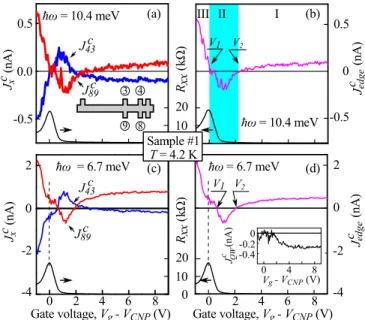
is clearly detectable. The same results have been obtained for the smaller contact spacing of 2.8μm between contacts 5–4 [see inset of Fig.3(a)], for whichG∼2e2/ hholds. The circular photocurrentsJxc=[J(σ+)−J(σ−)]/2, obtained for two frequencies, are displayed in Figs.4(a)and4(c).
The fact that edge currents at opposite sample sides have opposite polarities allows us to refine the edge current contribution Jedgec by subtracting the currents measured at opposite sides,Jedgec =(J43c −J89c)/2. Corresponding data are shown in Figs.4(b)and4(d). By summing up the currents, JQWc =(J43c +J89c)/2, we obtain the bulk contribution which is shown in the inset of Fig. 4(d). Remarkably, the sign of Jedgec changes twice: at a gate voltage close to the CNP
FIG. 4. (a) and (c) Circular photocurrents Jxc obtained at the opposite edges, see inset of (a). Black solid curves show the resistance measured between the contacts 3 and 4. (b) and (d) Edge and QW bulk (inset) contributions.
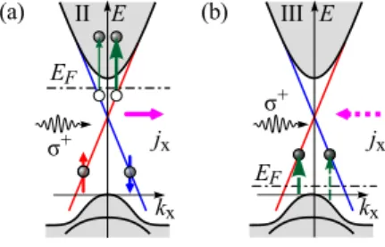
FIG. 5. Schematic picture of optical transitions and the edge photocurrent formation for two positions of the Fermi level. Region II:Ec−EF<hω. Region III:¯ EFis close to the valence band top.
and atVg−VCNP ≈2 V, while the bulk contributionJQWc is noticeable only for larger gate voltages. Similar results are obtained for all samples. Data from the second wafer are shown in the Supplemental Material [24]. The central result so far is that we can selectively excite left- and right-moving edge currents by means of the photon helicity, in accordance with the helical nature of these states. Below we resort to a microscopic model to understand the origin of the photocurrents in the different gate voltage regions, marked by I to III in Fig.4(b).
Region II corresponds to the gate voltages between the nodes of the photocurrent. Note that the border between regions II and III is close to the CNP.
In region I, i.e., atVg−VCNP>2 V, the Fermi level lies in the conduction band, as it follows from transport measurement, seeRxx in Fig.4(b). Here both bulk and edge photocurrents are formed by conduction band carriers. The low symmetry results in an asymmetric scattering of carriers causing an edge photocurrent with the direction determined by the radiation helicity. This mechanism has been explored before in graphene and other 2D materials [25,26] and is also active here.
IfEFis in the bulk gap the above mechanism is no longer effective and the presence of topological edge states needs to be taken into account to explain the current formation.
Figure5illustrates the linear dispersion of helical edge states.
The edge states with the positive velocity along x direction are formed mainly from|E1,+1/2and|H1,+3/2subbands and have pseudospin s= +1/2 (spin-up branch) [27,28].
Counterpropagating electrons haves= −1/2.
The Fermi level crosses the bottom of the conduction band and enters the bulk gap at a gate voltage of ≈2 V. This corresponds to region II displayed in Fig. 5(a). While the bulk photocurrent ceases, see inset of Fig. 4(d), the edge photocurrent changes polarity, rises, and exhibits a maximum atVg−VCNP≈1 V. From the fact thatEFis in region II in the bulk gap and the photon energy is smaller than the gap we conclude that the photocurrent is caused by optical transitions involving helical edge states in the gap. Different transitions are conceivable including those between edge and bulk states, direct transitions between the spin-up and spin-down branches of the linear edge state spectrum, and indirect transitions.
Different transitions are conceivable including those between edge and bulk states, direct transitions between the spin-up and spin-down branches of the linear edge state spectrum, and indirect transitions. Direct optical transitions between the spin-up and spin-down branches have a low probability.
Moreover, the photocurrent caused by such transitions would
have a maximum for the Fermi energy lying at the Dirac point and would vanish for large negative or positive gate voltages, which is not the case. Photocurrents caused by the Drude-like free-carrier absorption require additional scattering and k-dependent velocity and, therefore, seem to be weak.
Comparing the efficiencies of all these processes we attribute the circular edge photocurrents in region II to the excitation of electrons from helical edge states to bulk conduction band states (“photoionization” of the edge channels) [29,30].
We note that in HgTe/CdHgTe QWs, localized electron states might exist in the gap (e.g., charge puddles also close to edges) being discussed as a possible source of backscattering in helical channels [31–33]. These topologically trivial states can enhance the Drude absorption and thus photocurrents in helical edge channels. They can also give rise to an additional edge photocurrent not involving helical channels. However, the corresponding contributions are expected to be weak because the density of trivial states localized at edges is much smaller than that of helical states. This conclusion is supported by the fact that the photoresponse signatures obtained for the shortest contact separation (with quantized conductance heralding the dominance of helical edge states) are essentially the same as for larger separations.
The generation of photocurrent via the edge-to-bulk exci- tation is schematically shown in Fig. 5(a) [34,35]. Vertical arrows represent the photoionization of helical states, i.e., the depopulation of Dirac states and population of excited bulk states with nonzero transverse wave vectors ky. For the excitation with σ+ radiation the probability of optical transitions from the states with s=1/2 is larger than that involving the states with s= −1/2. This is illustrated in Fig.5(a) by arrows of different thickness. Microscopically, this imbalance of optical transition rates stems from the electron-hole asymmetry, see Ref. [29] and the Supplemental Material [24]. The resulting imbalance of the edge state populations leads to a net electric current jx [36]. For σ− radiation the transitions from the spin-down states dominate and the photocurrent reverses. The photocurrent is excited in the rangeEc−hω < E¯ F< Ec+hω¯ [37]. The range of EF and, respectively, the range of gate voltages for which this photocurrent is generated, increases with increasing ¯hω.
Exactly such a behavior is observed in experiment, see Figs.4(b),4(d), and1(a).
The selection rules described above yield
g+1/2(kx)−g−1/2(−kx)
g+1/2(kx)+g−1/2(−kx) =KPcirc, (1)
where g±1/2 are the probabilities of transitions from initial states with s= ±1/2, K is the coefficient describing the rigidity of the selection rules, andPcircis the radiation helicity.
Our calculations show thatK, determined by band structure parameters, depends only weakly on kx and the photon energy ¯hω(Supplemental Material see Ref. [24]). In a simple four-subband model with inversion center, the coefficientK at kx =0 is given by 2BD/(B2+D2) [29], where B and Dare the parameters of the Bernevig-Hughes-Zhang (BHZ) Hamiltonian [2].
FIG. 6. (a) Circular edge photocurrents measured in region II.
(b) Calculated edge currents as a function ofEFcounted from the Dirac point.
Calculations within the relaxation time approximation yield the following expression for the edge current:
jx = −eKPcirc 2πh¯
τp(ε)gtot(ε)dε, (2) where τp is the momentum relaxation time determined by backscattering processes for edge carriers, and gtot(ε)= g+1/2+g−1/2 is the total probability of photoionization of electrons with energyεby circularly polarized radiation [38].
Figure6 compares the calculated currents with measured ones for photon energies ¯hω=6.7 and 10.4 meV. A magnified view of the data is shown in Figs. 4(b) and 4(d). In the calculations we assume that τp(ε) is a steplike function:
τp=20 ps for energies in the band gap, which is estimated from the length of the ballistic transport edge≈2.8μm in our devices and the edge state velocity∼107cm/s, andτp =0.3 ps for energies above the conduction band bottom, which is estimated from the bulk mobility. It is seen that with a decrease of the photon energy the photocurrent peak narrows. Moreover, the signal amplitude for ¯hω=6.7 meV is higher than that for
¯
hω=10.4 meV. The photocurrent increase is caused by an increase of the photon density at fixed radiation intensity and increase the probability of edge-to-band optical transitions, see the Supplemental Material [24]. Figure6(b)shows that the the-
ory describes the dependencies of the photocurrent onVg and the radiation frequency quite well. Moreover, the calculated magnitude of the current is close to the experimental values.
Finally, we discuss region III. This region corresponds to negative gate voltages where EF is shifted towards the valence band. Similarly to region II, we attribute the observed photocurrent to transitions from the valence band to the edge states, see Fig.5(b). This mechanism of photocurrent formation is essentially the same as in region II. The question, though, is why the photocurrent direction reverses. To describe the current direction for a given helicity correctly one needs to assume that the selection rules for optical transitions are reversed, i.e., the transitions to the s= +1/2 edge states occur now dominantly forσ+radiation. This, however, is at odds with the BHZ model. In fact, this is not surprising. The valence band structure of 8-nm-wide HgTe QWs is known to be strongly affected by the closely lying excited|H2subband not included in the BHZ model, which results in a nonmonotonic dispersion of the hole states and the formation of side maxima [39]. The current reversal may be also related to a strong energy dependence of the momentum relaxation time. A calculation of the optical transitions and the photocurrent requires the detailed knowledge of the real band structure and optical transitions beyond the BHZ model and will be done elsewhere.
To summarize, our results demonstrate that excitation of HgTe 2D TIs by circularly polarized terahertz radiation results in a dc electric current flowing in helical edge channels. This observation provides a novel access for probing spin transport in TIs.
We thank G. V. Budkin for helpful discussions. The support by the DFG (Grant No. SPP 1666), Elite Net- work of Bavaria (Grant No. K-NW-2013-247), the Volk- swagen Stiftung Program, and the RFBR (Projects No.
15-02-06344, No. 16-02-01037, No. 16-32-00540, and No. 16-32-60175) are gratefully acknowledged. The re- search of Novosibirsk group was supported by RSF (Grant No. RSF-16-12-10041).
[1] C. L. Kane and E. J. Mele, Phys. Rev. Lett. 95, 226801 (2005).
[2] B. A. Bernevig, T. L. Hughes, and S. C. Zhang,Science314, 1757(2006).
[3] M. Z. Hasan and C. L. Kane,Rev. Mod. Phys.82,3045(2010).
[4] X.-L. Qi and S.-C. Zhang,Rev. Mod. Phys.83,1057(2011).
[5] M. König, S. Wiedmann, C. Brüne, A. Roth, H. Buhmann, L. W. Molenkamp, X.-L. Qi, and S.-C. Zhang,Science318, 766(2007).
[6] A. Roth, C. Brüne, H. Buhmann, L. W. Molenkamp, J. Maciejko, X.-L. Qi, and S.-C. Zhang,Science325,294(2009).
[7] G. M. Gusev, Z. D. Kvon, O. A. Shegai, N. N. Mikhailov, S. A.
Dvoretsky, and J. C. Portal,Phys. Rev. B84,121302(R)(2011).
[8] K. C. Nowack, E. M. Spanton, M. Baenninger, M. König, J. R.
Kirtley, B. Kalisky, C. Ames, P. Leubner, C. Brüne, H. Buhmann, L. W. Molenkamp, D. Goldhaber-Gordon, and K. A. Moler,Nat.
Mater.12,787(2013).
[9] M. König, M. Baenninger, A. G. F. Garcia, N. Harjee, B. L. Pruitt, C. Ames, P. Leubner, C. Brüne, H. Buhmann,
L. W. Molenkamp, and D. Goldhaber-Gordon, Phys. Rev. X 3,021003(2013).
[10] E. Y. Ma, M. R. Calvo, J. Wang, B. Lian, M. Mühlbauer, C. Brüne, Y.-T. Cui, K. Lai, W. Kundhikanjana, Y. Yang, M.
Baenninger, M. König, C. Ames, H. Buhmann, P. Leubner, L. W.
Molenkamp, S.-C. Zhang, D. Goldhaber-Gordon, M. A. Kelly, and Z.-X. Shen,Nat. Commun.6,7252(2015).
[11] S. Hart, H. Ren, T. Wagner, P. Leubner, M. Mühlbauer, C. Brüne, H. Buhmann, L. W. Molenkamp, and A. Yacoby,Nat. Phys.10, 638(2014).
[12] C. Brüne, A. Roth, H. Buhmann, E. M. Hankiewicz, L. W.
Molenkamp, J. Maciejko, X.-L. Qi, and S.-C. Zhang,Nat. Phys.
8,486(2012).
[13] A. Kononov, S. V. Egorov, Z. D. Kvon, N. N. Mikhailov, S. A.
Dvoretsky, and E. V. Deviatov,JETP Lett.101,814(2015).
[14] S. D. Ganichev, E. L. Ivchenko, and W. Prettl,Physica E14, 166(2002).
[15] S. D. Ganichev and L. E. Golub,Phys. Status Solidi b251,1801 (2014).
[16] Z. D. Kvon, S. N. Danilov, N. N. Mikhailov, S. A. Dvoretsky, and S. D. Ganichev,Physica E40,1885(2008).
[17] S. A. Dvoretsky, N. N. Mikhailov, Y. Sidorov, V. Shvets, S. N.
Danilov, B. Wittman, and S. D. Ganichev,J. Electron. Mater.
39,918(2010).
[18] For different sample cooldowns, the CNP can occur at different gate voltages. This is caused by the to cooldown dependent charge trapping in the insulator.
[19] S. D. Ganichev, S. A. Tarasenko, V. V. Bel’kov, P. Olbrich, W. Eder, D. R. Yakovlev, V. Kolkovsky, W. Zaleszczyk, G.
Karczewski, T. Wojtowicz, and D. Weiss,Phys. Rev. Lett.102, 156602(2009).
[20] C. Drexler, S. A. Tarasenko, P. Olbrich, J. Karch, M. Hirmer, F. Müller, M. Gmitra, J. Fabian, R. Yakimova, S. Lara-Avila, S.
Kubatkin, and S. D. Ganichev,Nat. Nanotechnol.8,104(2013).
[21] E. Ziemann, S. D. Ganichev, I. N. Yassievich, V. I. Perel, and W. Prettl,J. Appl. Phys.87,3843(2000).
[22] P. Schneider, J. Kainz, S. D. Ganichev, V. V. Bel’kov, S. N.
Danilov, M. M. Glazov, L. E. Golub, U. Rössler, W. Wegschei- der, D. Weiss, D. Schuh, and W. Prettl,J. Appl. Phys.96,420 (2004).
[23] P. Olbrich, J. Karch, E. L. Ivchenko, J. Kamann, B. März, M.
Fehrenbacher, D. Weiss, and S. D. Ganichev,Phys. Rev. B83, 165320(2011).
[24] See Supplemental Material athttp://link.aps.org/supplemental/
10.1103/PhysRevB.95.201103 for additional data detected in samples produced from a second waver and details of the spin- dependent optical selection rules and the theory of the edge photocurrent. Furthermore, we present a power dependency of the edge current and measurements in the presence of a magnetic field.
[25] J. Karch, C. Drexler, P. Olbrich, M. Fehrenbacher, M. Hirmer, M. M. Glazov, S. A. Tarasenko, E. L. Ivchenko, B. Birkner, J.
Eroms, D. Weiss, R. Yakimova, S. Lara-Avila, S. Kubatkin, M.
Ostler, T. Seyller, and S. D. Ganichev,Phys. Rev. Lett.107, 276601(2011).
[26] M. M. Glazov and S. D. Ganichev, Phys. Rep. 535, 101 (2014).
[27] M. V. Durnev and S. A. Tarasenko,Phys. Rev. B93,075434 (2016).
[28] S. A. Tarasenko, M. V. Durnev, M. O. Nestoklon, E. L.
Ivchenko, J.-W. Luo, and A. Zunger,Phys. Rev. B91,081302(R) (2015).
[29] V. Kaladzhyan, P. P. Aseev, and S. N. Artemenko,Phys. Rev. B 92,155424(2015).
[30] L. I. Magarill and M. V. Entin,JETP Lett.104,771(2016).
[31] J. I. Väyrynen, M. Goldstein, and L. I. Glazman,Phys. Rev. Lett.
110,216402(2013).
[32] B. L. Altshuler, I. L. Aleiner, and V. I. Yudson,Phys. Rev. Lett.
111,086401(2013).
[33] S. Essert and K. Richter,2D Mater.2,024005(2015).
[34] Note that the model involves similar physical concepts as used for describing photocurrents due to intersubband transitions in semiconductor QWs [35].
[35] S. D. Ganichev, V. V. Bel’kov, Petra Schneider, E. L. Ivchenko, S. A. Tarasenko, W. Wegscheider, D. Weiss, D. Schuh, E. V.
Beregulin, and W. Prettl,Phys. Rev. B68,035319(2003).
[36] Note that the photoexcited carriers in the conduction band also contribute to the photocurrent but this contribution is small due to fast momentum relaxation of bulk carriers.
[37] The edge current based on the photoionization picture requires that the initial states of the optical transitions are occupied and the final ones are empty and that the energy conservation holds.
In real structures, the window is somewhat broadened due to inhomogeneities of the structures.
[38] We assume that the spin relaxation of bulk carriers is fast and, therefore, photoexcited carriers get unpolarized before they are trapped back on helical edge states. This means that the depopulation of edge states determines the photocurrent.
[39] G. M. Minkov, A. V. Germanenko, O. E. Rut, A. A. Sherstobitov, M. O. Nestoklon, S. A. Dvoretski, and N. N. Mikhailov,Phys.
Rev. B93,155304(2016).