Transition metal impurities in wide bandgap oxides: fundamental model systems for strongly correlated oxides
I n a u g u r a l - D i s s e r t a t i o n zur
Erlangung des Doktorgrades
der Mathematisch-Naturwissenschaftlichen Fakult¨ at der Universit¨ at zu K¨ oln
vorgelegt von
Tim Jakobus Thomas Haupricht aus K¨ oln
K¨ oln 2011
Berichterstatter:
Prof. Dr. L. H. Tjeng Prof. Dr. T. Michely
Tag der m¨ undlichen Pr¨ ufung:
03.02.2011
Abstract
Most of the modern electronic devices are still based on the electrical prop- erties of metals and semiconductors. Yet, the transition metal oxides show a variety of spectacular physical effects like, e.g., high-temperature supercon- ductivity, the giant or tunnel magneto resistance, spin-polarized transport, metal to insulator transitions, or multiferroic order. If ways could be found to make use of these phenomena, one could obtain devices with unprece- dented functionalities. This, however, requires a profound understanding of the electronic structure of these compounds. Electron-electron correlations are very important here, thereby requiring a more sophisticated theoretical ansatz. An effective first order approach to take these correlation effects into account is to neglect the translational symmetry of the real crystal and to describe the electronic structure in a local single-site impurity model. This is done for example in the so-called configuration-interaction cluster calcula- tions where the system is reduced to a single ion and its ligands, and also, at least for the correlations, in dynamical mean-field theory (DMFT). The underlying idea is that the ground state and near ground state properties as well as the excitation spectra can be described on an equal footing as far as the many body aspects are concerned. It is not always easy, however, to judge about the applicability of the results for the real bulk systems. An experimental test is highly desired.
In this thesis we have, therefore, set out to study the electronic structure
of selected transition metal impurities in oxides using photoemission (PES)
and x-ray absorption spectroscopy (XAS). We have simulated our experi-
mental data using a single-site cluster model and compare the results to the
respective bulk systems. We found that transition metal impurities in oxides
are fundamental model systems to study the electronic structure of strongly
correlated oxides. A detailed study of their electronic structure yields essen-
tial information on the importance of local and non-local interactions in the
associated bulk compounds and even more complicated materials.
Kurzzusammenfassung
Die Funktionsweise moderner elektronischer Ger¨ ate basiert noch immer weitestgehend auf den elektronischen Eigenschaften von einfachen Metallen und Halbleitern. ¨ Ubergangsmetalloxide hingegen weisen eine Vielzahl spek- takul¨ arer physikalischer Eigenschaften auf. So zeigen Sie z.B. Hochtem- peratursupraleitung, den Riesen- oder Tunnelmagnetwiderstand, Spin- polarisierten Transport, Metall-Isolator ¨ Uberg¨ ange oder multiferroische Ord- nung. Die technische Nutzung dieser Ph¨ anomene w¨ urde einen Zugang zu Ger¨ aten mit nie dagewesenen Eigenschaften erm¨ oglichen. Diese allerdings erfordert ein tiefgehendes Verst¨ andnis der elektronischen Struktur dieser Verbindungen. Elektron-Elektron Wechselwirkungen sind hier sehr aus- gepr¨ agt und erfordern eine anspruchsvollere und detailliertere theoretische Behandlung. In einem weit verbreiteten und sehr erfolgreichen Ansatz zur Ber¨ ucksichtigung dieser Korrelationseffekte wird die Translationssymmetrie eines realen Kristalls vollkommen vernachl¨ assigt. Stattdessen wird die lokale elektronische Struktur einer einzigen isolierten St¨ orstelle beschrieben. Diesen Ansatz verfolgen sog. configuration-interaction Clusterrechnungen, in denen der Festk¨ orper auf ein einzelnes Ion nebst den dazugeh¨ origen Liganden re- duziert wird. Die zugrunde liegende Idee ist, dass hier Grundzustands- und Nahgrundzustandseigenschaften sowie Anregungsspektren im Hinblick auf Korrelationseffekte gleichberechtigt behandelt werden k¨ onnen. Auch eine der am weitesten fortgeschrittenen Methoden der theoretischen Festk¨ orper- physik, die dynamische Mean-Field Theorie (DMFT), basiert auf diesem Ansatz. Trotzdem ist es oft nicht leicht zu beurteilen, wie gut die Ergebnisse und Modellparameter auf reale, ausgedehnte Systeme ¨ ubertragbar sind. Ein experimenteller Test w¨ are daher sehr w¨ unschenswert.
Diese Arbeit besch¨ aftigt sich aus diesem Grund mit der Untersuchung der elektronischen Struktur von ¨ Ubergangsmetall-St¨ orstellen in Oxiden mit- tels Photoemissions- (PES) und R¨ ontgenabsorptionsspektroskopie (XAS).
Die gewonnenen experimentellen Daten wurden im Rahmen von Clusterrech-
nungen simuliert, und die Ergebnisse mit den zugeh¨ origen Volumensystemen
verglichen. Es wird gezeigt, dass ¨ Ubergangsmetall-St¨ orstellen in Oxiden als
fundamentale Modellsysteme zur Untersuchung der elektronischen Struktur
stark korrelierter Oxide dienen k¨ onnen. Ihre detaillierte Untersuchung liefert
essentielle Informationen ¨ uber den Einfluss lokaler und nicht-lokaler Wechsel-
wirkungen in den zugeh¨ origen Volumensystemen oder weitaus kompliziert-
eren Verbindungen.
Contents
Abstract i
Kurzzusammenfassung iii
Abbreviations vii
1 Introduction 1
1.1 Correlated electron systems . . . . 1
1.2 Configuration-interaction cluster calculations . . . . 7
1.3 Scope of this thesis . . . . 11
2 Experimental methods 13 2.1 Molecular beam epitaxy . . . . 14
2.2 X-ray absorption spectroscopy . . . . 17
2.3 Photoemission spectroscopy . . . . 22
2.4 Synchrotron radiation . . . . 27
3 Non-local screening in NiO 31
4 Fe
2+impurities in MgO 45
5 Mn
2+impurities in MgO 59
6 V
3+impurities in Al
2O
369
7 V
2O
3thin films on Al
2O
379
Summary 85
Zusammenfassung 89
Bibliography 92
Acknowledgements 109
Erkl¨ arung 113
Publications 115
Abbreviations
XAS X-ray absorption spectroscopy
(I)PES (Inverse) Photoemission spectroscopy XPS X-ray photoemission spectroscopy HAXPES Hard x-ray photoemission spectroscopy MBE Molecular beam epitaxy
UHV Ultra-high vacuum
CI Configuration-interaction DFT Density functional theory DMFT Dynamical mean-field theory L(S)DA Local (spin-)density approximation
DOS Density of states
NSRRC National Synchrotron Radiation Research Center
MIT Metal to insulator transition
Chapter 1 Introduction
This thesis deals with the investigation of the electronic structure of transi- tion metal impurities in oxides. It will be shown how these impurity systems can be used as fundamental model compounds for (usually much more com- plicated) correlated electron systems, and to test the reliability of recent elec- tronic structure theories. Therefore, in this first introductive chapter we will briefly outline the most important physical concepts of strongly correlated electron systems and some basic ideas of a popular method of the local elec- tronic structure calculation for these compounds, namely, the configuration- interaction cluster model. In Section 1.3 the key issues and aims of this thesis will be introduced.
1.1 Correlated electron systems
One of the key problems in modern technology is to find proper materials for new applications and devices. Most modern electronics is still based on the transistor invented in the 1940s by Schockley, Bardeen, and Brattain [1].
1These transistors make use of the charge degree of freedom of the electron.
Since then it is one of the key issues in the design of integrated electronic circuits to increase the number of transistors per area. Today’s micropro- cessors are built from 32 nm structures produced using extreme ultraviolet (EUV) lithography [2]. This is already very close to the physical limit of integration which is in the order of a few ˚ A, the size of single atoms. Modern materials research tries to make also use of other properties of the electron, like, e.g., the spin and the orbital degrees of freedom. The ordering of these charge, orbital, and spin degrees of freedom, their fluctuations, interactions, and coupling to the crystal lattice lead to a variety of phenomena. New ef-
1W. B. Shockley, J. Bardeen, and W. H. Brattain, Nobel Prize in 1956
fects like high-T
csuperconductivity
2, giant magneto resistance (GMR)
3and tunnel magneto resistance (TMR) [3], spin-polarized electron transport [4, 5], or metal to insulator transitions [6] have been found from which part of them are already used in modern devices. In so-called multiferroics two or more ferroic phases appear simultaneously, opening a path to multi-functional ma- terials, very interesting with respect to device miniaturization [7]. In order to understand all these effects or, in the second step, to develop new materials or compounds for applications, a profound comprehension of the underlying physics and the electronic structure is indispensable. Unfortunately, most of these effects can no longer be explained by one-electron theory. Electron- electron interactions play a major role here, and thus electrons cannot be described as embedded in a static mean-field generated by the other electrons [8]. Due to the importance of these correlations, such systems are referred to as correlated electron systems. In this field of fundamental research binary transition metal monoxides are often regarded as “simple” model systems for more complicated compounds containing more elements in different environ- ments. However, most of these binary transition metal monoxides are by far not that simple as they might appear at first sight.
It was kind of a starting point of correlated electron physics when de Boer and Verwey [9] pointed out that many of the properties of the 3d transition metal compounds do not agree with the predictions of band theories. In basic classes of solid state physics we learn that [10]: “In the ground state of an insulator all bands are either completely filled or completely empty; in the ground state of a metal at least one band is partially filled.” Thus, from a band theory point of view, systems with an incompletely filled 3d shell should be a metal. Standard density-functional theory (DFT) [11, 12] predicts FeO, CoO, and CuO to be metallic [13, 14], for MnO and NiO a (way too small) bandgap is found, but only in the magnetically ordered phase [13, 15, 16].
Experimentally, all of these compounds have been found to be insulators with bandgaps between about 1 and 4 eV. In DFT calculations this problem could be fixed by the inclusion of a so-called self-interaction-correction term into the model, which than gives reasonable values for the bandgap [17]. How- ever, even though DFT methods have shown to give a good description of the ground state properties of many systems with weak correlation effects [17], they usually fail to reproduce excitation spectra such as x-ray absorp- tion and photoemission. Configuration-interaction cluster calculations [18]
and combined photoemission/ inverse-photoemission experiments [19] have pointed out the importance of the d-d Coulomb interaction U for the elec-
2J. G. Bednorz and K. A. M¨uller, Nobel Prize in 1987
3A. Fert and P. Gr¨unberg, Nobel Prize in 2007
tronic structure of correlated electron systems.
These electron-electron interactions have been used to explain the insu- lating state of a so-called Mott insulator. In his model, Mott considered a lattice with one single electronic orbital on each site. Electrons are now al- lowed to hop between these sites and each site can be occupied by up to two electrons. However, since two electrons would feel a large Coulomb repul- sion if they occupy the same site, the band will split into two: a lower lying band from electrons that occupy an empty site and a higher lying band from electrons occupying a site that is already taken by another electron. At half filling, i.e., one electron per site, the lower band is full and the system is an insulator. A first theoretical description of the transition from a Mott insu- lator to a metal was given within the Hubbard model which is the inclusion of interaction effects into a tight-binding description. The Hamilton operator of the Hubbard model is given by [20]
H = − t
∑⟨i,j⟩
c
†iσc
jσ+ U
∑i
n
i↑n
i↓(1.1)
and describes the competition between the kinetic energy (hopping) which favors the electrons to be delocalized over the lattice and the Coulomb repul- sion that drives the electrons to localize on the lattice sites (Mott insulator).
The first term in 1.1 describes the kinetic energy: An electron is annihilated at site j and created at site i, accompanied with the gain of the kinetic energy t, the strength of the hopping integral.
∑⟨i,j⟩here is a shorthand notation for the sum over neighboring lattice sites. The second term in 1.1 includes the number operator n
iσand describes the Coulomb repulsion. For double occupation the system has to pay the on-site repulsion U . So far the Hub- bard model has been exactly solved only in the limits of one dimension [21]
or infinite-range hopping [22]. However, it is already very interesting to look at the limiting cases: For U = 0 we are back in the tight-binding model with non-interacting electrons. For t = 0 or U/t = ∞ we have no hopping at all and, thus, a lattice of isolated atoms. For U ≫ t the band splits into a lower and a upper Hubbard band (see above).
However, for d electron systems orbital degeneracy is important and must
be taken into account. In transition metal compounds the overlap of d bands
and p bands of the ligands upon hybridization is also crucial. This led to
the distinction of two types of insulators, depending on the character of the
first electron removal and addition states. Figure 1.1 schematically explains
the difference between the electronic structure of a Mott-Hubbard (a) and
a charge-transfer (b) insulator. For a Mott-Hubbard insulator, the partially
filled d band is split by the d-d Coulomb repulsion U into a completely filled
lower Hubbard band and an empty upper Hubbard band - the material is
(a) Mott-Hubbard insulator (b) Charge-transfer insulator
Fig. 1.1:
Schematic illustration of the electronic structure of a (a) Mott-Hubbard and a (b) charge-transfer insulator. The insulating phase is driven by the
d-dCoulomb repulsion
U. (Reproduced from Ref. [6])
an insulator. If on the other hand, the charge-transfer energy ∆ is much smaller than U , the lower Hubbard band falls below the ligand p band. The insulating gap is then between the ligand p and the upper Hubbard band.
The system is called a charge-transfer insulator. For both scenarios, ∆ and U are defined in terms of energy differences between configurations as
∆ = E(d
n+1L) − E(d
n), (1.2)
U = E(d
n+1) + E(d
n−1) − 2E(d
n), (1.3) where E(d
n) is defined as the total energy of a d
nconfiguration and L denotes a ligand hole.
The concept of Mott-Hubbard and charge-transfer insulators has been generalized by Zaanen, Sawatzky, and Allen [23]. Their results is summarized in the phase diagram in Fig. 1.2. Here, compounds are classified dependent on the parameters U , ∆, and the ligand p and transition metal 3d hybridiza- tion parameter T . The heavy solid line (E
gap= 0.5 T ) here separates metals from insulators. In region (A) one finds Mott-Hubbard insulators. ∆ is much larger than U , and thus E
gap∝ U . Charge-transfer insulators are found in region (B), where U ≫ ∆ and E
gap∝ ∆. In the intermediate region (AB)
∆ and U are of comparable strength. For materials falling into this region the density of states close to the Fermi level is of highly mixed ligand 2p and transition metal 3d character.
Note that electron-electron correlation effects as described above are not
small or only important in very complicated systems. They already play
an essential role in one of the easiest systems than one can imagine: In the
hydrogen molecule (H
2) we consider two electrons in s-like orbitals, two sites,
and the hopping probability t. Within a one-electron picture one finds the
Fig. 1.2:
Zaanen, Sawatzky, and Allen (ZSA) phase diagram, estimating the char- acter of material (metal/insulator) dependent on the strength of the
d-dCoulomb repulsion
Uand the charge-transfer energy ∆. The heavy solid line (E
gap= 0.5
T)represents the separation between metals and semiconductors. (Reproduced from Ref. [23])
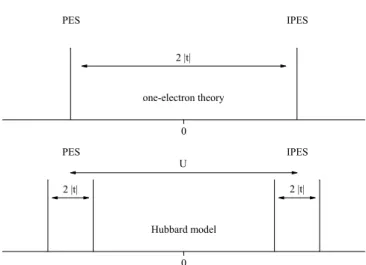
0
PES IPES
2 |t|
one-electron theory
0 Hubbard model
U
PES IPES
2 |t| 2 |t|
Fig. 1.3:
Schematic photoemission and inverse photoemission spectra and
bandgap of the H
2molecule within one-electron theory (top) and the Hubbard
model (bottom).
well-known bonding and anti-bonding states at E
0± t. Thus, in the ground state both electrons will occupy the bonding state with opposite spins. PES and IPES spectra would yield a single peak, respectively, separated by the bandgap E
g= 2 | t | (see Fig. 1.3). When we treat this system within the Hubbard model with U ≫ t, however, the bands split up in a lower and upper Hubbard band, and the PES and IPES spectra show two peaks each.
Within the spectra the two peaks are separated by ∆E = 2 | t | , the bandgap is E
g= U − 2 | t | + 2δ, where δ = 4t
2/U . The intensity ratio of the two peaks of the PES/IPES spectrum turns out to depend on the ratio t/U . Even though it is very simple, the hydrogen molecule model has been used to estimate t/U for real systems such as Ti
2O
3, a d
1system with a pronounced dimerization in the crystal structure [24].
As outlined above, standard band theory is not able to fully describe the
electronic structure of systems in which electron-electron correlations are im-
portant. The Hubbard model captures well the basic concept of correlations
but its simplifications are severe. Another approach is to concentrate on
the local electronic structure. Configuration-interaction cluster calculations
which usually treat a cluster of a transition metal ion surrounded by the lig-
ands in the correct symmetry turned out to be extremely useful to simulate
excitation spectra such as x-ray absorption or photoemission [25, 26, 27]. On
the other hand these kind of calculations are not ab initio and thus depend
on parameters which have to be estimated from experiments or different the-
oretical approaches. Since they are impurity calculations, long range crystal-
lographic order and intersite effects are also neglected here. New approaches
like the dynamical mean-field theory (DMFT) try to combine the advantages
of density-functional theory and impurity calculations: Here, the translation
invariant lattice of atoms in a solid is replaced by a single impurity atom that
resides in a bath of electrons. In contrast to common DFT methods here the
bath is not static. The central atom fluctuates between certain atomic con-
figurations with a certain probability. DMFT becomes exact in the limit
of infinite lattice coordination. In practice, DMFT and DFT methods are
often combined: Weakly correlated electrons are described within the LDA
approach and strongly correlated electrons are treated using DMFT. The re-
sulting Hamiltonian can then be solved with this LDA+DMFT method in a
self-consistent way [8]. However, also (single-site) DMFT is often not able to
reproduce details of experimental data such as intersite correlations or multi-
plet structures (cf. Chapter 3). Recent multi-site cluster and DMFT models
are a another promising step towards electronic structure calculations of real
materials.
1.2 Configuration-interaction cluster calcula- tions
Fig. 1.4:
Cluster of a transition metal cation (blue) surrounded by an octahedron of six oxygen anions (red), here in
Ohsymmetry. Illustrated using [28]
A cm
3of a material in the solid state contains about 10
24electrons which can principally interact whith each other. This makes an exact theoretical treatment of the electronic structure of a real solid impossible. Standard band theory makes use of the translational symmetry of crystals and then treats a single electron in the mean-field potential of all other electrons. Electron- electron interactions are completely neglected here. However, despite of these rather strong restrictions, many (ground state) properties of solid state ma- terials, in particular those of metals, can be very well understood within this one electron model.
A completely different approach is to neglect the translational symmetry of the crystal completely and to concentrate on the local correlations. In this impurity or cluster ansatz one restricts oneself to the description of one or a very limited number of ions residing in the surrounding of their ligands in the correct local symmetry. This restriction allows in principle to take all correlations explicitly into account, even the full atomic multiplet theory.
This model is in particular interesting for systems with narrow shells, such
as transition metal (3d) or rare earth (4f ) compounds. Here, the spread of
the radial wave functions is rather limited suggesting that the electrons may
mostly retain their local character. Since within this method the ground
state, low-lying excited states, and final states due to excitations can be
treated on equal footing it is particulary interesting for the simulation of
excitation spectra such as photoemission or x-ray absorption. In these cases the cluster model turned out to be very powerful [25, 29].
In this work configuration-interaction cluster calculations have been per- formed for the simulation of experimental x-ray absorption and photoemis- sion data. For the calculations we have used the XTLS 8.30 code by Arata Tanaka [25]. In this section some of the basic concepts of the cluster ap- proach will be illustrated. For more detailed information we refer to Refs.
[25, 26, 30, 31].
Talking about a (single-site) cluster we here refer to a transition metal ion surrounded by six O
2−ligands in the respective symmetry (see Fig. 1.4).
When hybridization is taken into account the ground state of a d
nsystem can be described as:
| i ⟩ = α
1| d
n⟩ + α
2| d
n+1L ⟩ + α
3| d
n+2L
2⟩ + ...,
where L means a ligand hole and
∑iα
i2= 1. The cluster is then treated using the following Hamiltonian:
H = H
1+ H
2, H
1=
∑i
ϵ
d(Γ
i)
∑γi
d
†γid
γi+
∑i
ϵ
p(Γ
i)
∑γi
p
†γip
γi+ ϵ
c∑ξ
c
†ξc
ξ+ U
dd∑i,j
∑
γi̸=γj
n
dγin
dγj− U
dc∑i,γi
n
dγi∑ξ
(1 − n
cξ)
+
∑i
V (Γ
i)
∑γi
(d
†γip
γi+ h.c.), H
2= H
dd+ H
dc+ H
d(ζ
d) + H
c(ζ
c).
In H
1the six different terms denote
1. The energy of the 3d orbit of the transition metal ion, where { Γ
i} stands for the corresponding representations of the respective symmetry group (t
2gand e
gin the case of O
h) and γ
iis the basis of each representation including the spin state.
2. The energy of the ligand molecular orbit.
3. The energy of the core orbit. Here, ξ denotes the orbital and spin state of the core orbit.
4. The effective 3d-3d interaction U
dd.
5. The attractive core-hole potential acting on the 3d electron U
dc.
6. The hybridization between the ligand and the 3d orbit.
H
2describes the full-multiplet 3d-3d (H
dd) and 3d-core (H
dc) interaction, expressed in terms of Slater integrals, and the spin-orbit coupling in the 3d (H
d(ζ
d)) and core (H
c(ζ
c)) state. (cf. [25])
Depending on the spectrum that one wants to simulate the final state wave function then is:
3d valence band PES: | f ⟩ = β
1| d
n−1⟩ + β
2| d
nL ⟩ + β
3| d
n+1L
2⟩ + ... , core level PES: | f ⟩ = β
1| cd
n⟩ + β
2| cd
n+1L ⟩ + β
3| cd
n+2L
2⟩ + ... ,
XAS: | f ⟩ = β
1| cd
n+1⟩ + β
2| cd
n+2L ⟩ + β
3| cd
n+3L
2⟩ + ... . Again, c and L denote a core and ligand hole, respectively, and
∑iβ
i2= 1.
The input parameters of a cluster calculation, therefore, typically are:
• The initial and final state configurations taken into account.
• Crystal field and hybridization, generally expressed in coefficients of an expansion in spherical harmonics. The crystal field can be, e.g., deter- mined by LDA(+U) calculations but is often fitted to the experimental data. This is possible since for systems with a high local symmetry the number of parameters needed is only very small (only one for O
hsymmetry, see below). Hybridization is usually calculated within the tight-binding model by Slater and Koster [32]. Here, the basis set used in the calculation can be significantly reduced by taking only the bond- ing orbitals into account.
• The Coulomb repulsion U and charge transfer energy ∆ as defined in Sec. 1.1.
• The spin-orbit coupling parameters ζ
dand ζ
c.
• The Slater integrals F
dd2and F
dd4, and F
cd2, G
1cdand G
3cddescribing the electron-electron interaction. The Slater integrals and spin-orbit coupling parameters are usually calculated within the Hartree-Fock approximation and are tabulated for a variety of elements, e.g., in Refs. [25, 30]. In a solid the Slater integrals are partially screened and are, thus, typically reduced to about 80% of the (atomic) Hartree-Fock value [33].
In this work systems with a cubic (O
h), tetragonal (D
4h), or trigonal (D
3d) local symmetry are treated. In the O
hcase the crystal field splits the 3d states into the well-known t
2gand e
gstates. This splitting can be described by one single parameter only, namely, the cubic crystal field splitting 10Dq.
See Fig. 1.5. A distortion of the O
hoctahedron of the ligands along one of
Spherical Cubic Tetragonal Trigonal =25Dq
2
+9/4D 2
+25/4D 2
-5DqD +25/3DqD -15/2D D
0
e g
: 6Dq
t 2 g
: -4Dq
e g
: -4Dq -Ds +4Dt b
2 g
: -4Dq +2Ds -Dt a
1 g
: 6Dq -2Ds -6Dt b
1 g
: 6Dq +2Ds -Dt
e g
: Dq +1/2D +3/2D + 1 / 2
e g
: Dq +1/2D +3/2D - 1 / 2 a
1 g
: -4Dq -2D -6D
Fig. 1.5:
Splitting of the
dorbitals in an octahedral, tetragonal, and trigonal field (cf. [30, 34]).
the principal axes leads to a D
4hlocal symmetry in which the t
2gand e
gstates are further split by additional parameters ∆t
2gand ∆e
g. Following Ballhausen [34], these splittings are described by introducing the parameters Ds and Dt, with ∆t
2g= 3Ds − 5Dt and ∆e
g= 4Ds + 5Dt. When the distortion of the octahedron is applied along the [111] direction we have a D
3dlocal symmetry. Here, the trigonal crystal field lifts the degeneracy of the t
2gand splits these into a non-degenerate a
1gand a doubly degenerate e
πgstate. For the description of the crystal field splitting in trigonal symmetry three parameters, usually called Dq, Dσ, and Dτ is needed, as well. These parameters are often re-expressed in terms of a so-called bare trigonal field D
trig0= − 3Dσ − 20Dτ /3 and a mixing term V
mix= √
2(Dσ − 5Dτ /3) which mixes the t
2gand e
gstates of the cubic field and, thus, leads to the formation of the e
σgand e
πgstates. D
0trigis the crystal field splitting between the a
1gand e
πgstates in the absence of the stabilization of the e
πgdue to the mixing
of t
2gand e
gstates. In the XTLS 8.30 code the crystal field is expressed
in terms of spherical harmonics. In this notation the complete form of the
crystal field on the d orbitals in O
h, D
4h, and D
3dsymmetry is [30]:
V
Oh= 21DqC
40(θ, ϕ) + 21
√
5
14 Dq(C
44(θ, ϕ) + C
4−4(θ, ϕ)), (1.4) V
D4h= − 7DsC
20(θ, ϕ) + 21(Dq − Dt)C
40(θ, ϕ) (1.5)
+21
√
5
14 Dq(C
44(θ, ϕ) + C
4−4(θ, ϕ)), V
D3d= − 7DσC
20(θ, ϕ) − 14(Dq + 3
2 Dτ )C
40(θ, ϕ) (1.6)
− 14
√
10
7 Dq(C
43(θ, ϕ) + C
4−3(θ, ϕ)), where C
lm(θ, ϕ) =
√2l+14πY
lm(θ, ϕ).
Finally, excitation spectra are usually calculated within the dipole ap- proximation. One has to diagonalize the initial and final state Hamiltonians and then to calculate the excitation probability to each final state. This gives a set of energies with the respective weights that, after taking a reasonable lifetime and experimental broadening into account, can be compared to ex- perimental spectra. A comparison of the parameter set found from a fit to experimental data to parameters from other experiments or calculations is, however, not always easy. The parameters from a fit to valence band PES data can be considerably different from those from a fit to, e.g., core level PES data of the same compound. This is because in the latter the param- eters are used in the presence of a core hole which can screen the strength of, e.g., crystal fields, hybridization, or hopping integrals in the final state [35, 36].
1.3 Scope of this thesis
As outlined above, configuration-interaction cluster calculations are very suc- cessful for the simulation of excitation spectra and the local electronic struc- ture of correlated electron systems. On the other hand they are impurity calculations that neglect the translational symmetry of a real crystal and, since they are not ab initio, depend on parameters. One could, therefore, imagine that the parameter set that one finds by fitting a cluster simulation to experimental data of bulk samples is kind of effective in the sense that it may compensate for differences originating from shortcomings of the model.
Also (single-site) DMFT treats correlations in an impurity ansatz, thereby
neglecting all possible non-local interactions. A natural approach to test the
validity of the cluster model and the physical meaning of its parameters would
be to investigate real impurity systems. Here, a single-site model should work perfectly, and parameters found from these simulations should be more meaningful. In the past, work on optical absorption spectra and electron spin resonance experiments on dilute crystalline salts of transition metals has already shown to yield valuable information about the energy levels, the ligand fields, and possible distortions [37, 38, 39, 40]. Modern spectroscopic techniques together with the availability of synchrotron radiation now allow us to investigate their electronic structure with unprecedented detail. We have, therefore, set out to systematically study the electronic structure of transition metal impurities in oxide host materials using x-ray absorption (XAS) and photoemission spectroscopy (PES). We have simulated the ex- perimental results using a single-site cluster approach. Depending on the investigated system the impurity approach allows to study various physical effects which will be shown for different examples: The impurity approach allows to eliminate intersite or non-local effects in the electronic structure.
Hence, details in the local electronic structure can be separately studied (cf.
Chapter 3 and 6). It gives the possibility to prepare model systems which are not stable as bulk compounds (cf. Chapter 4). By using impurity systems instead of the stoichiometric bulk compound one can induce changes in the local environment of the transition metal ions like, e.g., the strength of the ligand field (cf. Chapter 5).
However, in order to do these experiments, we still have to overcome an experimental problem. The host materials that one would typically use for transition metal oxide impurity systems (like MgO or Al
2O
3) are very good insulators and, therefore, not suitable for electron spectroscopic experiments.
They would immediately cause charging problems. Yet, we decided to pre-
pare the impurity systems as thin films on metal substrates using molecular
beam epitaxy (MBE). It is known from other studies [41] that, if the oxide
film is thin enough, the conducting substrate can provide electrons to neu-
tralize the sample charging. Furthermore, with MBE one operates far from
equilibrium conditions which allows to prepare model systems which are not
stable as bulk compounds. In addition, the in situ preparation and direct
characterization using spectroscopy offers, in contrast to bulk crystal growth,
an online control of the growth parameters at the experiment (stoichiometry,
impurity concentration, etc.), an important aspect regarding time-limited ex-
periments (e.g., at synchrotron facilities). For clarity and better readability,
details of the electronic structure and the physical properties of the studied
compounds (or of the associated stoichiometric bulk crystals) and open ques-
tions therein will be introduced and discussed in the respective chapters. In
Chapter 2 the most important experimental techniques that were used for
the studies in this thesis will be explained.
Chapter 2
Experimental methods
In this Chapter the experimental techniques that were used for this work will be introduced. The explanation will be very general and concentrate on the basic concepts. Details that are important for certain experiments will be dealt with in the respective chapters.
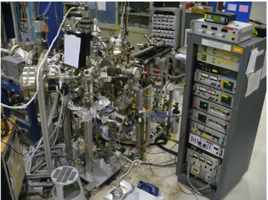
Fig. 2.1:
The Cologne combined XAS/PES and Mini-MBE setup installed at
the Dragon beamline of the National Synchrotron Radiation Research Center
(NSRRC) in Hsinchu, Taiwan
2.1 Molecular beam epitaxy
For several reasons most of the samples studied in this thesis have been prepared as thin films. Therefore, the most important nucleation processes and growth modes of thin films, and some details of molecular beam epitaxy will be discussed in the following.
In Fig. 2.2 the fundamental atomic processes for thin film growth on surfaces are shown. When single atoms or molecules from an evaporation source hit the substrate they may diffuse on the surface until one of the other processes shown in Fig. 2.2 sets in: They can nucleate to small clusters or at special sites such as defects or steps, but they can also diffuse into the substrate or even be re-evaporated. (cf. [42])
Fig. 2.2:
Relevant processes in nucleation and growth of thin films on surfaces.
(Reproduced from Ref. [42])
In epitaxy one distinguishes between different growth modes. The four
most important are illustrated in Fig. 2.3. When the impinging atoms or
molecules are stronger bound to the substrate than to each other one finds the
layer-by-layer growth mode, in which the next layer starts to form when the
previous one is already completed. In the other situation, namely the binding
of the impinging particles to each other is stronger than to the substrate, the
atoms nucleate as small clusters on the substrate surface and then grow into
islands of the condensed phase. This situation is called island growth. An
intermediate situation occurs if the binding energy to the substrate or the
previous layers changes in a non-monotonic way: In the Stranski-Krastanov
growth mode, the film grows in island-growth after the first monolayer(s)
have formed in a layer-by-layer fashion. A possible reason for such a change
in binding energy is, e.g., the reduction of stress due to lattice misfit by
island formation. In reality, substrates are usually not atomically flat but,
on a microscopic scale, show crystallographic imperfections such as disloca-
tions, defects, or steps. These sites are energetically favorable for impinging
atoms such that new layers start to form preferentially at steps (step-flow
growth). Which of the above mentioned growth modes appears for a certain
Fig. 2.3:
Sketch of the relevant growth modes for thin film growth. (Reproduced from Ref. [44])
system depends on many parameters such as, e.g., material fluxes, growth temperature, substrate quality, and lattice misfit to the substrate. (cf. [43]) In molecular beam epitaxy (MBE), materials are deposited from differ- ent sources (solids, gases) onto a substrate whose temperature can usually be controlled. This is done in ultra-high vacuum conditions (base pressures of MBE systems usually are in the order of 10
−10mbar), allowing for several advantages of this technique. The low residual gas pressure leads to a very long mean free path of atoms or molecules in the systems. Therefore, the mass flow from evaporation sources can be regarded as a directed beam. Fur- thermore, it allows for very clean thin films with very little impurities and outstanding crystalline quality. In ultra-high vacuum, one also operates far from thermodynamic equilibrium conditions. For this reason the kinetics of the above mentioned growth processes on surfaces become the most impor- tant parameters. This allows to prepare systems that are usually not stable at ambient pressure or whose preparation usually requires extreme process parameters like very high temperatures or pressures as it is the case, e.g., for the preparation of EuO [45]. The use of Knudsen cells or electron beam evap- orators, in which the source materials are heated by a tungsten filament or an electron beam, allows to precisely control the material fluxes. In this way, the growth of even sub-monolayer films is possible. The vacuum environment also gives the possibility for an in situ real-time control of the crystal growth using, e.g., reflection high energy electron diffraction (RHEED). (cf. [43])
All thin film samples for this work have been prepared using our so-called
Mini-MBE setup. A photograph of this machine, mounted in combination
with our XAS/PES measurement chamber at the Dragon beamline of the Na- tional Synchrotron Radiation Research Center (NSRRC) in Hsinchu, Taiwan is shown in Fig. 2.1. The Cologne Mini-MBE setup consists of a cylindrical main chamber which can be equipped with up to three evaporators. An Ar sputter gun and a heating stage can be used for substrate cleaning and an- nealing. The manipulator/ sample holder allows to heat the sample to up to 500
◦C. Oxygen gas can be introduced as molecular O
2via a leak valve or, if needed, as radical oxygen ions via a thermal gas cracker. The system further features a reflection high energy electron diffraction system (RHEED) for sample surface crystal structure analysis during growth.
The Mini-MBE setup is directly connected to a combined XAS/PES mea-
surement chamber (see Fig. 2.1), thereby allowing for an all in vacuo charac-
terization of the freshly grown films. These two techniques for the character-
ization of the microscopic electronic structure of the sample will be explained
in the following two Sections.
2.2 X-ray absorption spectroscopy
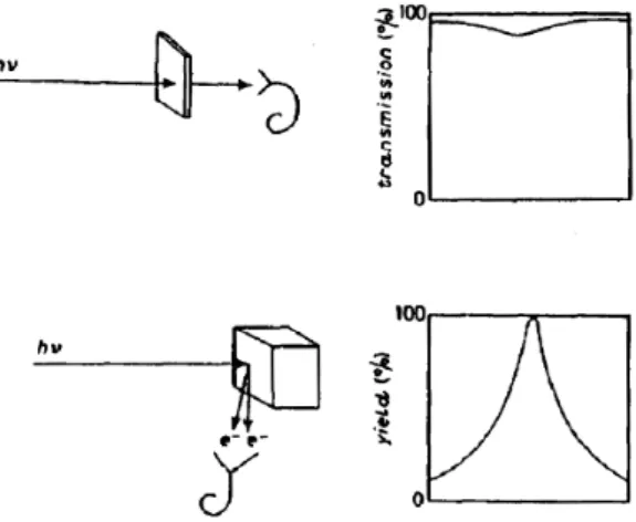
In x-ray absorption spectroscopy (XAS) one measures the photon energy dependent absorption of x-rays of a sample. This can basically be done in two different ways, as it is shown in Fig. 2.4: In the transmission mode, the transmitted x-ray intensity if compared to that of the incoming light.
Due to the rather strong absorption of x-rays by matter, the transmission mode is often not applicable. On the other hand, one can also measure the absorption of x-rays using the yield mode. Here, secondary effects are used to measure the absorption cross section. Upon relaxation from the photo-excited state, fluorescence photons, Auger electrons, photoelectrons, and even ions are emitted from the sample. All of them are supposed to give a signal that is proportional to the absorption cross section [46]. The most frequently used detection mode is the so-called total electron yield (TEY).
Here, the drain current of the sample, which is the net current of all charged particles emitted, is measured with high accuracy. The probing depth of the TEY is about 40 ˚ A [29]. In the energy-selected or partial electron yield (PY) one measures emitted electrons within a certain kinetic energy window [47]. Depending on the selected energies, the PY is very surface sensitive and probes only a few ˚ A of the sample. The ion yield mode measures only ions emitted from the surface [48]. The ion yield mode is the most surface sensitive detection technique and probes only the surface (2 ˚ A [29]). The most bulk-sensitive detection mode is the fluorescence yield (FY) [49], where emitted fluorescence photons are detected using a diode, a micro-channel
Fig. 2.4:
Schematic representation of an x-ray absorption experiment performed
in the transmission (top) and yield (bottom) detection mode. (Reproduced from
Ref. [29])
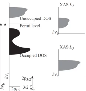
Fig. 2.5:
Interpretation of x-ray absorption spectra within an one-electron picture:
The experimental spectrum is a convolution of the delta-shaped core levels with the unoccupied density of states. (Reproduced from Ref. [30])
plate, or a channeltron. Since the attenuation length of photons in matter is much larger than that of charged particles, the probing depth of FY is comparably large (> 1000 ˚ A [29]).
The basic mechanism of XAS is rather simple. When a sample is irradi- ated by light with an energy equal to the binding energy of a certain core level, electrons can be excited to the lowest lying unoccupied states, as it is illustrated using a single-electron model in Fig. 2.5. The interaction of x-rays with matter can here be described by Fermi’s golden rule stating that the probability W of a system for a transition between initial state Ψ
iand final state Ψ
fis given by [50]:
W = 2π
¯
h |⟨ Ψ
f| T | Ψ
i⟩|
2δ(E
f− E
i− ¯ hω). (2.1) Here, E
iand E
fare the total energies of the initial and final states, and T is the transition operator. Re-writing the latter within the dipole approxi- mation leads to:
W ∝
∑q
2π
¯
h |⟨ Ψ
f| ˆ e
q· r | Ψ
i⟩|
2δ(E
f− E
i− ¯ hω). (2.2)
The dipole operator is only non-zero if the orbital quantum number of final
and initial state differ by 1, and the spin is conserved, thus, ∆L = ± 1 and
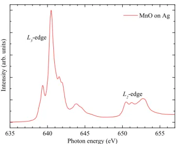
635 640 645 650 655 L
2 -edge
MnO on Ag
Intensity(arb.units)
Photon energy (eV) L
3 -edge
Fig. 2.6:
Isotropic Mn
L2,3x-ray absorption spectrum of MnO grown on Ag.
The line shapes of the
L3and
L2edge are very different and the branching ratio is larger than 2/3, already indicating the breakdown of the one-electron picture here.
∆S = 0. Quadrupole transitions are some hundred times weaker and can usually be neglected in XAS. For historical reasons, in XAS the main peaks are labeled as follows: The shell of the initial state is referred to as K (n = 1), L (n = 2), M (n = 3) etc.. For a given shell, the transitions are numbered consecutively starting from the lowest core level. Related to this work, the most interesting transitions are the transition metal L
2and L
3edges, which are transitions from the spin-orbit split 2p (2p
1/2and 2p
3/2) to empty 3d final states. The energy position of these transitions, of course, depends on the binding energy of the core electron and is, thus, strongly element specific.
For the 3d transition metals, the 2p core levels have binding energies between about 400 eV and 1000 eV.
Within this rather simple one-electron description and according to
Fig. 2.5, we would expect the L
2and L
3edges of an x-ray absorption spec-
trum to have the same shape and an intensity ratio I(L
3)/I(L
2+ L
3), the
so-called branching ratio [51], of 2/3. Comparing Fig. 2.5 and Fig. 2.6, which
shows the experimental Mn L
2,3spectrum of MnO as an example, one finds
that this is obviously not the case. Here, the L
2and L
3line shapes are
very different and the branching ratio is much larger than 2/3. This already
means that the one-electron picture is no valid description here. The reason
for this is that one actually does not observe the unoccupied density of states
in an XAS experiment. In the final state, the 2p core hole and the 3d valence
Fig. 2.7:
Cu
L2,3fluorescence yield x-ray absorption spectra of La
1.85Sr
0.15CuO
4for
E⊥c(dashed line) and
E∥c(solid line). (Reproduced from Ref. [52])
wave function have a strong overlap. They are strongly bound and form an exciton, i.e., a bound electron-hole pair, due to the strong 2p core hole to 3d electron attraction. This strong bond of the core hole leads to almost atomiclike final states, allowing for successfully describing most features of x-ray absorption spectra within a local model. On the other hand, this also means that the one-electron picture breaks down here: An exciton can only be explained in terms of a many-electron system. The underlying atomiclike physics is, however, very well known. Core hole and 3d electron both can be in different orbitals, respectively, leading to a large number of possible final states. The number of possible transitions is, however, reduced significantly by the application of the dipole selection rules (see above). The full atomic multiplet theory has to be taken into account. A pure atomic description of XAS is usually not sufficient. The ligands surrounding the probed ion will react on the presence of the core hole and have, thus, to be taken into account. The exact energy position and line shape of an x-ray absorption spectrum depends on the local environment of the probed ion. This makes XAS sensitive to the valence, spin-state, and ligand field symmetry.
When linear polarized x-rays and single crystal samples are used in an
XAS experiment, only electrons from orbitals which have a component par-
allel to the electric field vector E of the light can be excited. Furthermore,
these electrons can only be excited to orbitals with a component parallel to
E. The intensity thus depends on the occupation of these orbitals. This effect
is called linear dichroism and allows to directly probe the orbital occupation
using XAS. An example where this effect can be seen in a very distinctive
way is shown in Fig. 2.7. Here, the Cu L
2,3edges of La
1.85Sr
0.15CuO
4is shown
measured with E ⊥ c (dashed line) and E ∥ c (solid line). La
1.85Sr
0.15CuO
4is a layered compound, belonging to the high-T
ccuprate superconductors, in which the CuO
2planes are well separated by two LaO layers. In its tetrago- nal structure, the Cu ions (Cu
2+d
9) are surrounded by an octahedron of O ions, whose (out-of-plane) c-axis is considerably elongated compared to the a-axis. One would, therefore, expect the d
x2−y2orbital to be high in energy and thus unoccupied. Looking at Fig. 2.7, this is what one can indeed see:
For E ⊥ c electrons can be excited to the d
x2−y2hole. A strong absorp- tion edge is found. For E ∥ c there is no empty final state available. The absorption is consistently suppressed.
XAS also offers insight to magnetic properties of a sample. In x-ray mag- netic circular dichroism (XMCD) circular polarized light is used on magne- tized samples. Spectra taken using left- and right-circular polarized x-rays show a difference that gives information about magnetic moments of the probed ion. Sum rules have been derived [53, 54] which allow to comparably easily derive the orbital ⟨ L
z⟩ , spin ⟨ S
z⟩ , and dipole ⟨ T
z⟩ moment from the dichroic signal.
Summarizing, XAS is a synchrotron-based, site selective tool which is sen-
sitive to the valence, spin-state, and local environment of the probed ion. In
an one-electron approximation, it measures the unoccupied density of states
of a sample. For correlated systems, however, the core hole potential be-
comes dominant and a description including the full atomic multiplet theory
is necessary.
2.3 Photoemission spectroscopy
Fig. 2.8:
Schematic setup of a photoemission experiment: The sample is irra- diated by light of a certain energy and polarization. The kinetic energy of the emitted photoelectrons is then measured using an analyzer as a function of the emission angle
θand
ϕand the spin orientation of the electrons
σ. (Reproducedfrom Ref. [55])
Photoemission spectroscopy (PES) has been established as one of the most important methods to study the electronic structure of molecules, solids and surfaces [55]. In contrast to XAS, which probes partially filled or empty states, PES is used to study the occupied states of a sample.
Figure 2.8 schematically shows the basic concept of a photoemission ex- periment. When a sample is irradiated by light of an energy hν larger than the so-called work function Φ, electrons of the sample with binding energy E
Bcan be excited above the vacuum level and leave the sample (if they do not undergo inelastic scattering) with an kinetic energy
E
kin= hν − E
B− Φ.
This is Einstein’s famous equation [56], theoretically describing the photo- electric effect, which has been experimentally found earlier by Hertz [57] and Hallwachs [58]. From this rather simple equation one can already see that by measuring the kinetic energy of the photoelectrons (and knowing the photon energy and work function) one finds the binding energy of these electrons in the measured compound.
Nowadays, different kind of light sources are typically used for PES experi-
ments. Monochromatic ultraviolet line spectra from discharge lamps are used
in ultraviolet photoemission (UPS) to study valence band states with high energy resolution. Since laboratory light sources can be used, this method is comparably easy to handle, but the very high surface sensitivity has to be taken into account. In x-ray photoemission spectroscopy (XPS) monochro- matic x-ray sources such as Al or Mg K
αradiation are used as excitation sources. Compared to UPS, it is more bulk sensitive and allows to study core level spectra as well. XPS can be very well used for the chemical in- vestigation of surfaces, thin films, and bulk samples and is for this reason also known as ESCA (electron spectroscopy for chemical analysis). Using synchrotron light as excitation source for PES allows to make use of different photoionization cross sections and to adjust the probing depth by properly tuning the photon energy. Present-day synchrotron sources also allow to use hard x-rays for PES (HAXPES), thereby enhancing the probing depth sig- nificantly, which makes bulk sensitive measurements possible and simplifies the sample preparation.
Modern hemispherical electron spectrometers are able to measure pho- toelectrons with an sub-meV energy resolution, and also allow to map the emission angle by using appropriate electron lens systems. Angle-resolved photoemission spectroscopy (ARPES) gives direct insight to the dispersion of valence band states.
Figure 2.9 shows in a simplified one-electron picture how a photoemission spectrum is connected to the electronic structure of the sample. Here, the photoemission spectrum is a direct image of the occupied density of states, convoluted with an experimental resolution function. However, this simpli- fied picture is usually not valid for PES on systems where electron correlations play a role (see Sec. 1.1). Here, one should better think in terms of initial ( | i ⟩ ) and final state ( | f ⟩ ) configurations:
| i ⟩ = α
1| d
n⟩ + α
2| d
n+1L ⟩ + α
3| d
n+2L
2⟩ + ...
| f ⟩ = β
1| d
n−1⟩ + β
2| d
nL ⟩ + β
3| d
n+1L
2⟩ + ...,
for 3d valence band photoemission on a 3d
nsystem, where L denotes a ligand hole.
In a photoemission experiment the work function Φ, which is a character- istic of the analyzer, has to be found out experimentally by measurements on reference samples (typically scans of the Fermi edge of Ag or Au samples).
For photoemission experiments it is important to know that the photoion-
ization cross section (the probability of a photoelectron to be emitted from a
certain subshell when a photon is absorbed) can be very different for different
elements and (sub-)shells, and strongly depends on the photon energy used
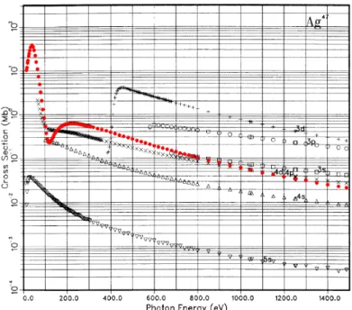
for excitation. The photoionization cross section has been calculated and
Fig. 2.9:
Simplified representation of the photoemission process using an one-
electron picture: An electron with binding energy
EBcan be excited above the
vacuum level by photons with energy
hν > EB+Φ
0, where Φ
0is the so-called work
function. The measured energy distribution of the photoelectrons then reflects, in
this simplified picture, the occupied density of states of the sample. (Reproduced
from Ref. [55])
tabulated for free ions [59]. However, one needs to take into account that it can principally be different in solids [60].
In Fig. 2.10 the calculated photon energy dependence of the photoioniza- tion cross section of Ag is shown. One can see that the cross section is very different for each subshell, and that it decreases with increasing photon en- ergy. However, the cross section of the Ag 4d shows a pronounced minimum at around 120 eV. This is a so-called Cooper minimum [61] that occurs due to vanishing matrix elements for certain transitions. As stated above, the pho- ton energy dependence of the cross section can be exploited in experiments to enhance or suppress certain features in photoemission spectra.
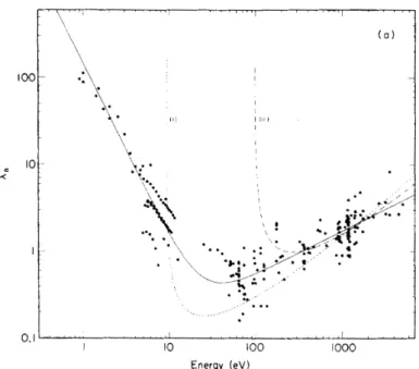
The high surface sensitivity of PES is due to the strong interaction of electrons with matter. The probability that a photoelectron undergoes in- elastic scattering on its way out of the sample is rather high and depends on its kinetic energy. It has been shown [62] that the resulting inelastic mean free path (IMFP) follows a so-called universal curve (see Fig. 2.11). This curve shows a minimum of only a few ˚ A between around 10 and 100 eV ki- netic energy. Note that the universality of the curve should be treated with attention. Even though it was experimentally shown to be valid for many el-
Fig. 2.10: