Recent Developments in Silicon Photomultipliers
Jelena Ninkovi´c
a,b,∗
aMax-Planck-Institute for Physics, F¨ohringer Ring 6, D-80805 Munich, Germany
bMax-Planck-Institute Semiconductor Laboratory, Otto-Hahn-Ring 6, D-81739 Munich, Germany
Abstract
A novel type of avalanche photodetector with Geiger mode operation, known as Silicon PhotoMultiplier (SiPM) represents an interesting advance in photodetection and is already an alternative to traditional PMTs in many applications. The state of the art of the SiPMs - their main properties and problems are discussed.
Key words: single photon counting, SiPM, BID SiPM PACS:85.60.Gz, 95.55.Aq, 42.50.Ar
1 Introduction
Development of photodetectors for the detection of low intensity pho- ton flux is one of the critical issues for experimental physics, medical to- mography and many other areas. In most of these applications as a pho- todetector standard PhotoMultiplier Tube (PMT) is used. PMTs have two main problems: they are very sensi- tive to the magnetic fields and have high price due to the complicated production process. The search for an alternative detector started long
∗ Corresponding author Email address:
ninkovic@mppmu.mpg.de(Jelena Ninkovi´c).
time ago. Promising candidate for the replacement of PMTs was the Avalanche PhotoDiode (APD). Al- though it has an internal gain it was not capable of detecting single pho- tons. At the beginning of this mil- lennium new detector concept was developed, the silicon photodetector operated in limited Geiger mode, ca- pable of detecting single photons like a PMT and therefore it got the name Silicon PhotoMultiplier (SiPM). For the past few years mainly Russian groups pursued the development of a new type of APD [1][2][3], but nowadays the interest for these de- vices is increasing and they are being developed on many places around the world. Recently, a new concept was introduced: A Back Illuminated
Drift SiPM (BID SiPM) where an APD is combined with a drift diode to form a building block for an ar- ray [4][5][6]. These devices are to be produces in Max-Planck-Institute Semiconductor Laboratory[7].
2 The Silicon Photomultiplier concept
A SiPM is an array of small APDs (cells) combined to form a macro- scopic unit (typically 500 to 4000 cells per mm2). Each cell operates in limited Geiger mode and a small polysilicon resistor, which connects the cell to a conductive grid, limits the current through the junction and quenches the avalanche once the cell capacity has been discharged. Single cells produce a standard signal when any of them goes to breakdown. In the SiPM the independent operat- ing APD cells are all connected to a common readout line. Therefore, the output signal is the superposition of the standardized signals of all fired cells. In the case of BID SiPM con- cept radiation enters from the back- side of a fully depleted wafer and the photoelectrons are focused (drifted) onto a small “point-like” avalanche region located on the front side.
3 SiPM properties
SiPM reaches an intrinsic gain for single photoelectrons at the level of
∼106 and the amplitude of a single cell is proportional to the capaci-
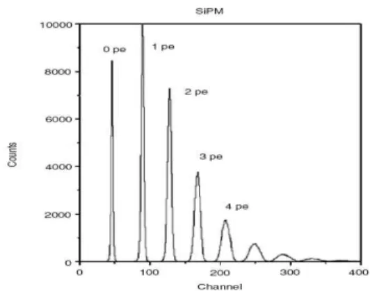
Fig. 1.Pulse height spectrum of light pulses with very low intensity recorded with a SiPM. Taken from Buzham et al. [11]].
tance of the cell times the overvolt- age (difference between the opera- tional voltage and the breakdown voltage).1 In case of not too intense light flashes, the number of fired cells is in first order proportional to the number of photons thus compensat- ing for the missing dynamic range of a single Geiger mode APD. For large light flashes saturation effects set in.
In reality, the process is more com- plex because of the recovery time of the cells and the influence of dark current. The main domain of opera- tion for SiPMs is for light levels with a photoelectron flux ≪1 photoelec- tron/cell/recovery time. These de- vices have an excellent photon count- ing capability (see figure 1) which comes as a consequence of good cell to cell gain uniformity, negligible contribution of electronic noise and very low excess noise factor of single cells.
Unfortunately, the breakdown can
1 It should be noted that two photoelectrons de- tected by single cell are producing same output signal as a single one. Therefore, one cannot dis- tinguish if one or more photoelectrons have been detected by a cell.
be triggered not only by an incoming photon but also by any generation of free carriers. The latter produces dark countswith a rate of 100 kHz to several MHz per mm2 at 25◦C and with a threshold at half of the one photon amplitude. Thermally gener- ated free carriers can be reduced by cooling. There is a factor 2 reduction of the dark counts every 8◦C-10◦C.
Another possibility is to operate at lower bias resulting in a smaller elec- tric field and thereby lower Geiger efficiency. Field-assisted generation (tunneling) can only be reduced by a smaller electric field. The dark counts can be reduced in the SiPM pro- duction process by minimizing the number of generation-recombination centers, the impurities and crystal defects. The BID SiPM is expected to have an increased dark rate due to the bigger active volume. In order to keep dark rate lower one has to maintain good technology and fur- ther reduction can be achieved with tinning down of devices.
One possible disadvantage for use of SiPM in many applications comes from the fact that in an avalanche breakdown there are in average 3 photons emitted per 105carriers with a photon energy higher than 1.14 eV [8][9][10]. When these photons travel to a neighboring cell they can trig- ger a breakdown there. This gives rise to the optical crosstalk which violates the pixel independence and leads to a non-Poissonian behavior of the distribution of the number of fired pixels, it acts like shower fluc- tuations in an APD. It is a stochas- tic process and introduces an excess noise factor like in a normal APD
or a PMT. With a dedicated design with implementation of grooves be- tween the cells, which act as an op- tical insulation, the crosstalk can be reduced. Since the concept of BID SiPM is based on point like high filed regions the cross talk effect for these devices should be reduced but final evaluation can be performed only after the first prototype production.
Timing properties of SiPMs, even for single photoelectrons, are excel- lent (FWHM of 123ps has been mea- sured for a single cell[11]) mainly be- cause the avalanche breakdown pro- cess is fast and the signal amplitude is big. Fluctuations in the avalanche are mainly due to a lateral spread- ing (∼10ps) by diffusion and by the photons emitted in the avalanche [8].
Operation at high overvoltage (high gain) may slightly improve the time resolution. For the BID SiPMs drift- ing of photoelectrons increases a time jitter. Reduction of a pixel size im- proves time jitter but increases the cross talk.
The photon detection efficiency (PDE) of SiPMs is in first-order the product of quantum efficiency of the active area (QE), a geometric factor (ratio of active to total area), the probability to initiate an avalanche breakdown (Geiger efficiency) and the fraction of active cells, i.e. those cells which are not quenched or are still recovering from a previous breakdown. QE is maximal 80-90%
depending on the wavelength. It peaks in a relative narrow range of wavelengths because the sensitive layer of silicon is very thin. Devices with n-silicon on a p-substrate are
300 400 500 600 700 800 900 1000 10-3
10-2 10-1 100 101 102 103
electrons trigger avalanche
Absorption length [µm]
Wavelength [nm]
holes trigger avalanche
1 2 3 4 5 6 7
100 101 102 103 104 105 106
E [V/cm]
X [µm]
holes electrons
Drift region Geiger region
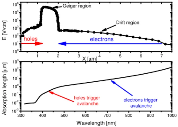
Fig. 2. Influence of difference in behavior of electrons and holes on the PDE. Top: Electric field distribution in epitaxial layer (after Buzhan et al. [12]). Bottom: Light absorption in Silicon.
more sensitive for green and red light and less for blue light because only the photons with longer wavelengths penetrate deep enough into the sil- icon (see fig. 2). Additionally, elec- trons have a higher Geiger efficiency compared to holes. Geometric factor is limited by the dead area around each cell, depends on the construc- tion and ranges typically between 20% and 70% of the total area. This is the parameter that can be opti- mized for specific application. Typ- ical values of PDE of recent SiPMs [13] are comparable to the QE of conventional bialkali photomultipli- ers. The main advantage of the BID SiPM concept is its expected PDE.
The geometrical fill factor of 100%
as well as non structured radiation entrance window, that allows de- position of different antireflective coatings [14][15][6], make this de- vice unique and superior compared to SiPMs. PDE as high as 85% at 400nm can be expected for these devices[6].
4 Conclusions
SiPMs are already now an alterna- tive to PMTs. They are the bet- ter choice for the detection of light with very low intensity when there is a magnetic field and when space and power consumption are limited.
Most of the devices are still small (1×1mm2...5×5mm2) but areas of 10×10mm2 are planed in the near future. The development started some 10 years ago but still there is a broad room for improvements.
Many parameters can be adjusted to optimize the devices and to tailor them for special needs. But one has to take into account that there are many cross-correlations which make it impossible to built a perfect de- vice, but compromises are necessary and a device has to be optimized for a specific application. For example trenches reduce crosstalk, which al- lows to increase the overvoltage im- proving PDE and UV response but still reducing the fill factor. For the use in PET, a high dark rate is un- critical, as one is interested in signals that exceed the one photoelectron level by a large margin while the in- tegration window is only a few tens of nanoseconds for fast scintillators.
For application in high energy as- trophysics, like MAGIC[16], devices with high PDE will increase the ef- fective sensitivity of the experiment and therefore lower the observational threshold, therefore the BID SiPM would be a better choice.
References
[1] B. Dolgoshein, et al., NIM A 504 (2003) 48–52
[2] V. Golovin, Patent No. RU 2142175, 1998 [3] Z. Sadygov, Patent No. RU 2102820, 1998 [4] G. Lutz et al.,IEEE Trans.Nuc. Sci. 52
(2005) 1156–1159
[5] G. Lutz et al., Proc. Int. Con. New Dev.
Photodet. Beaune (2005) to be published in NIM A
[6] J. Ninkovic et al., to appear in this proceedings
[7] MPI Halbleiterlabor,
http://www.hll.mpg.de/
[8] A. Lacaita et al.,IEEE TED 40(3) (1993) 577
[9] A. Lacaita et al., Apl. Phys. Letters 62 (1992)
[10] A. Lacaita et al., Apl. Phys. Letters 57 (1990)
[11] P. Buzhan, et al.,NIM A 504(2003) 48–52
[12] P. Buzhan, B.
Dolgoshein, et al., AN ADVANCED STUDY OF SILICON PHOTOMULTIPLIER, ICFA Instrumentation Bulletin, 2001
[13] B. Dolgoshein, presentation at LIGHT2006, to appear in NIM A
[14] R. Hartmann, K. Stephan and L. Strueder, NIM A 439(2000) 216-220
[15] R. Hartmann et al., Proc. SPIE 5903 (2005) N1-N9
[16] MAGIC experiment -
http://magic.mppmu.mpg.de/
[17] Golovin V., et al. NIM A 518 (2004), 560564