Silicon and Silicon Detectors
C. Betancourt Universit¨at Z¨urich
30.05.2018
1 / 20
Diamond Lattice Structure
Chapter 4. Silicon and silicon detectors 23
Figure 4.1: The diamond lattice structure, whereais the lattice constant [43].
solutions to Schr¨odinger’s equation of the form equation (4.2). These forbidden energy solutions will form gaps within the bands, and are referred asband gaps.
Thus, silicon, with its periodic diamond lattice structure, will also have a band structure characterized by its band gap. The band gap of silicon at a temperature ofT = 300 K isEg= 1.12 eV. The band structures for three of the most important semiconductors, germanium (Ge), silicon (Si) and gallium arsenide (GaAs), are shown in figure4.2.
The lower band is known as the valence band, and represents the energy of valence electrons bound to their parent atoms, while the upper band is known as theconduction band, and represents quasi-free states where electrons are free to move throughout the crystal. AtT = 0 K, the valence band will be completely occupied by valence electrons while the conduction band will be empty.
The bands are not constant, but vary with the wave vector. Semiconductors where the maximum of the valence band and minimum of the conduction band occur at the samekare known asdirectsemiconductors, while ones who’s valence band has a maximum and conduction band has minimum at di↵erentkare known as indirect semiconductors. Silicon is an indirect semiconductor, but for most practical purposes it is useful to consider a simplified band picture where the bands are constant, as seen in figure 4.3. Here the valence band is denoted EV
and the conduction bandEC.
The electrical conductivity of a material will depend on the size of the band gap. Insulatorsare materials who’s band gap is very large, typically several eV, which lead to very low electrical conductivity. Conductors are materials whose energy bands overlap or where partial filling of the conduction band is seen already at T = 0 K, and will have very high electrical conductivity. Semiconductors are then materials whose bands do not overlap, but have a band gap smaller than that of insulators, typically on the order of an eV.
2 / 20
Band Diagram
Chapter 4. Silicon and silicon detectors 24
Figure 4.2: The band structure as a function of the wave vector for Ge, Si, and GeAs, whereEg is the band gap energy [43].
Figure 4.3: A simplified band diagram of a semiconductor.
3 / 20
Direct vs. Indirect SemiconductorChapter 4. Silicon and silicon detectors 24
Figure 4.2: The band structure as a function of the wave vector for Ge, Si, and GeAs, whereEg is the band gap energy [43].
Figure 4.3: A simplified band diagram of a semiconductor.
4 / 20
Covalent Bonds and Doping
16 CHAPTER 1. PHYSICS AND PROPERTIES OF SEMICONDUCTORS-A REVIEW
GaAs 1.519 5 . 4 ~ 1 0 - ~ 204 1.169 4.9~10" 655
Fig. 6
T (K)
Energy bandgaps of Si and GaAs as a function of temperature. (After Refs. 22-23.)
1.4 CARRIER CONCENTRATION AT THERMAL EQUILIBRIUM
One of the most-important properties of a semiconductor is that it can be doped with different types and concentrations of impurities to vary its resistivity. Also, when these impurities are ionized and the carriers are depleted, they leave behind a charge density that results in an electric field and sometimes a potential barrier inside the semiconductor. Such properties are absent in a metal or an insulator.
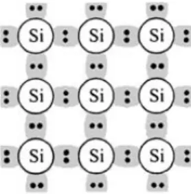
Figure 7 shows three basic bond representations of a semiconductor. Figure 7a shows intrinsic silicon, which is very pure and contains a negligibly small amount of impurities. Each silicon atom shares its four valence electrons with the four neigh-
:@:&@: .. ..
t..*
*...
(a) (b) (c)
Fig. 7 Three basic bond pictures of a semiconductor. (a) Intrinsic Si with no impurity. (b) n-type Si with donor (phosphorus). (c)p-type Si with acceptor (boron).
5 / 20
Defects
Chapter 4. Silicon and silicon detectors 26
6.2 Defects at the Interface 87
E
CE
VE
T1e
-e
-e
-e
-h
+h
+E
(1) (2)
(3) (4)
Fig. 6.1.A representation of the four exchange mechanisms at the interface states:
(1) electron capture, (2) electron emission, (3) hole capture, and (4) hole emission (adapted from Barbottin et al. [41])
unavailable. The section summarizes some of the popular models for interface states and for fixed interface charges.
6.2.3.1 Model of Interface States based on Defects in SiO
2One of the interface state model attributes interface states to the deep trap centers in SiO
2[41]. This model identifies the trap centers in SiO
2that are located close to the interface to be a source of interface states, and the defects centers that are unaltered by an external signal are a source of fixed oxide charges. Based on this model, a possible candidate for an interface state is the color center, called the B
2center, in SiO
2. The B
2band lies at 5.1 eV above the E
Vof SiO
2, and is close to the E
Cof Si, as shown in Fig. 6.2.
Consequently, if the B
2center is located close to the interface, it is likely to interact with the carriers in the Si conduction band and behave like an interface state.
6.2.3.2 Models of Interface States based on Interface Atoms and Disorder
Models that are based on the assumption that interface states are due to in- terface atoms have continually evolved, and have facilitated the development of an interface state model that provides good agreement with the experimen- tal results. Some of the more prevalent models in this category include: the disordered interface model, the dangling bond model, the P
bcenter model, and the trivalent silicon model.
The disorder interface model suggests that the disorder at the interface, related to the formation of Si-OH and trivalent Si groups, can result in donor and acceptor centers that act as interface states. This model incorporates the fact that the interface state density, D
it, depends on the orientation, oxidation rates, and annealing behavior [41].
Figure 4.4: An illustration of the four competing processes governing the occupancy of defect states [45].
electrons is then determined by
nt = Ntf(Et) = Nt
1 +e(Et EF)/kT (4.4)
and that of trapped holes
pt =Nt(1 f(Et)) = Nt
1 +e (Et EF)/kT. (4.5) In general1, the charge state of defects will depend on four competing processes as seen in figure4.4[46, 47]
1. capture of an electron from the conduction band: r1 =ennt
2. emission of an electron into the conduction band: r2 =cnnpt
3. capture of a hole from a valence band: r3 =cppnt
4. emission of a hole into the valence band: r4 =eppt
Hereri represents the rate for process i,n and pare the respective concentration of free electrons and holes in the conduction and valence bands,enand ep are the emission ratesfor electrons and holes, andcnandcpare thecapture coef f icients for electrons and holes. The emission rates and capture coefficients are related by en,p =cn,pe±(EC,V Et)/kTNC,V (4.6) where NC,V represents the number of free states in the conduction and valence bands. Thecapture cross section for electrons and holes can be defined as
n,p = cn,p/¯vn,p (4.7)
1This means not necessarily in thermal equilibrium, such as in a steady state or high injection conditions.
6 / 20
The P-N junctionChapter 4. Silicon and silicon detectors 29
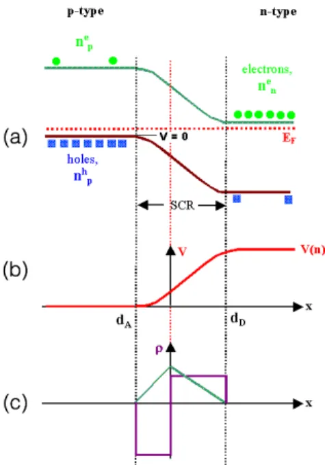
Figure 4.5: An illustration of a p-n junction showing (a) the energy band diagram, (b) the resulting built-in voltage and (c) the charge density within the
space charge region.
Let us first consider the case of an intrinsic semiconductor. For such a mate- rial, the Fermi energyEF will lie in the middle of the band gap, half way between the valence and conduction bands. As donors are added, the Fermi energy will shift upwards towards the conduction band. Conversely, adding acceptors will shift the Fermi energy down towards the valence band. So for n-type material, the Fermi energy lies near the conduction band, and for p-type material it lies close to the valence band. When the two materials come into contact, their Fermi energy of the two will not match. In order for the system to be in thermal equilibrium, a constant Fermi energy throughout the whole system is required. This leads to electrons from the n-type material di↵using into the p-type material and holes from the p-type material di↵using into the n-type material until a constant Fermi energy is achieved throughout. The bands will be shifted with respect to each other in the two materials, and the region around the junction being depleted of free charge carriers. This region is known as thedepletion region, or more appro- priately thespace charge region, and consists of fixed ionized impurities stripped of their quasi-free charge carriers. The space charge region constitutes the active region of the device. The shift in bands also leads to a potential drop called the built-in voltage. The entire process is illustrated in figure4.5.
The current-voltage characteristics of a p-n junction were first derived by Shockley3[50]. The current in a p-n junction as a function of the applied external
3The derivation depends on four main assumptions: (1) the junction is abrupt; (2) the Boltz- mann relation holds in the depletion region; (3) the injected concentration of minority carries is
7 / 20
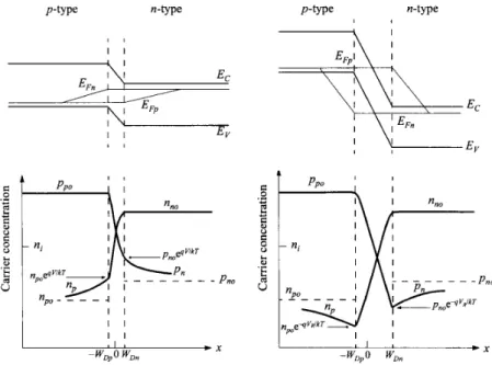
Carrier transport92 CHAPTER 2. p-n JUNCTIONS
1 1
P"0
Fig. 8 Energy-band diagram, with quasi-Fermi levels for electrons and holes, and carrier dis- tributions under (a) forward bias and (b) reverse bias.
Eqs. 48a and 48b, and to the current as given by Eqs. 50 and 5 1. Inside the depletion region, EFn and EFp remain relatively constant. This comes about because the carrier concentrations are relatively much higher inside the depletion region, but since the currents remain fairly constant, the gradients of the quasi-Fermi levels have to be small. In addition, the depletion width is typically much shorter than the diffusion length, so the total drop of quasi-Fermi levels inside the depletion width is not signif- icant. With these arguments, it follows that within the depletion region,
q V = EFn-EFp, (52)
Equations 49 and 52 can be combined to give the electron density at the boundary of the depletion-layer region on thep-side (x = - WDp):
where pp = p for low-level injection, and npo is the equilibrium electron density on the p-side. Similarly, P O
8 / 20
Current-Voltage
2.3 CURRENT-VOLTAGE CHARACTERISTICS 95
Equation 63 is the celebrated Shockley equation,',2 which is the ideal diode law. The ideal current-voltage relation is shown in Figs. 10a and b in the linear and semilog plots, respectively. In the forward direction (positive bias on the p-side) for V > 3kT/q, the rate of current rise is constant (Fig. lob); at 300 K for every decade change of current, the voltage changes by 59.5 mV (= 2.3kTlq). In the reverse direc- tion, the current density saturates at - J,.
We shall now briefly consider the temperature effect on the saturation current density J,. We shall consider only the first term in Eq. 64, since the second term will behave similarly to the first one. For the one-sided p+-n abrupt junction (with donor concentration ND),p >> npo, the second term can also be neglected. The quantities n , Dp,pno, and Lp (= &p) are all temperature-dependent. If Dp/7p is proportional to
TY, where yis a constant, then
The temperature dependence of the term T(3+"2) is not important compared with the exponential term. The slope of a plot J, versus l/Tis determined mainly by the energy gap Eg. It is expected that in the reverse direction, where lJRl = J,, the current will increase approximately as exp(-E$kT) with temperature; and in the forward direc- tion, where JF = J,exp(qV/kT), the current will increase approximately as exp[Wg - 4 v)lkTl.
xward
I I , I I ./ I I I I 1 )
-5 qVlkT
Reverse
IJJJol 104 103 102 10' 1 lo-'
Fig. 10 Ideal current-voltage characteristics. (a) Linear plot. (b) Semilog plot.
9 / 20
Silicon Detectors
Chapter 4. Silicon and silicon detectors 32
1.3 Working Principle of a Silicon Tracking Device 25
n++ layer n-bulk
n++ ring
n++ ring
strip p+ impl
ants
passivation SiO2 oxide
DC-pad AC-pad bias ring
guard ring
bias resistor
coupling capacity oxide SiO2
vias
vias
Al strips p+ impl
ants
aluminium backplane alignment
marker
passivation opening s
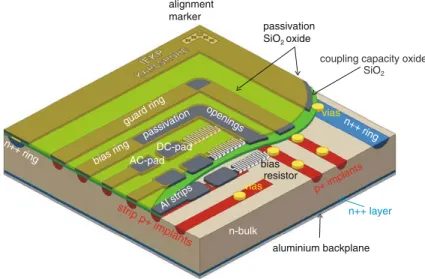
Fig. 1.19 A 3D schematic is sketched. It shows the baseline of the CMS sensor at the LHC in 2008, but could represent basically any single-sided AC-coupled, Rpolybiased sensor. In operation, the bias ring is connected to GND potential, which is then distributed to the p+implant strips, while the Al backplane is set to positive high voltage depleting the full n-bulk volume by forming a pn-junction p+strip to n-bulk. The coupling capacitor is defined between aluminium strip and p+implant, the inter-strip capacity between neighbouring strips (both p+and Al part). The guard ring shapes the field at the borders. The n++ring defines the volume and prevents high field in the real cut edge regions
All individual isolated strips need to be at the same potential. This is realized in one of three different ways, illustrated in Fig. 1.20, although nowadays the polysili- con method is most utilized.15
p+ p+
n+
Al strip
Al backplane n-bulk SiO2
bias ring polysilison resistor DC pad polysilicon biasing
p+ p+
n+
Al strip
Al backplane n-bulk SiO2
bias DC pad ring
punchthrough biasing small gap
p+ p+
n+
Al strip
Al backplane n-bulk SiO2
bias DC pad ring
FOXFET biasing gate
Fig. 1.20 There are three ways to bias an AC-coupled sensor plus a fourth one for a DC-coupled device. The punchthrough and FOXFET biasing are the easiest ones but not as radiation hard as the polysilicon resistor, which is more or less the current standard. A photo of a polysilicon resistor can be seen in Fig. 1.28. In addition, a DC-coupled device can be biased via the connections to the electronics, representing the ground potential
15Punchthrough and FOXFET biasing is less radiation hard, it can be imagined for the future InternationalLinearCollider (ILC).
Figure 4.6: A schematic of a typical silicon strip detector [52].
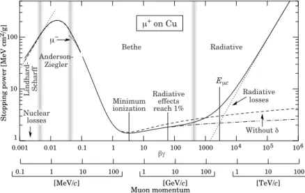
by the Bethe-Bloch formula dE
dx = 4⇡NAr2emec2z2Z A
11 2ln
✓2mec2 2 2Tmax
I2
◆
2 ( )
2 (4.25)
wherezis the charge of the incoming particle,Tmaxthe maximum kinetic energy that can be imparted to an electron during a collision,I the average excitation energy,Zthe atomic number,Athe atomic mass,NAAvogadro’s number,methe mass of the electron,cthe speed of light,rethe classical electron radius, =v/c,
= 1/p
1 2and the density e↵ect correction. The full function for the case muons traversing copper is shown in figure4.7. The most important part of the curve occurs at the minimum, which represents the minimum ionization energy in the material. Particles with an energy at the minimum are termed Minimum Ionizing Particles (MIPs). For silicon, the average energy loss is 390 µmeV, which, given that the energy needed to create an electron-hole pair is 3.6 eV, leads to an average number of 108 electron-hole pairs being created for eachµm. The full function of the Bethe-Bloch formula is shown in figure4.7.
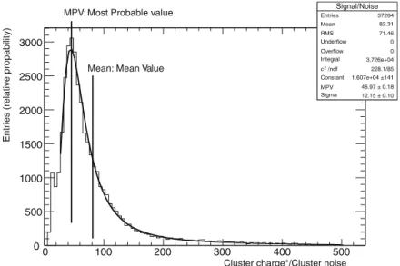
The most probable value (MPV) of the deposited charge is less than the aver- age due to statistical fluctuations that can be described bystraggling f unctions.
These straggling functions are described by a Landau distribution, which also takes into account noise contributions which tend to broaden the spectrum, which can be seen in figure4.8. For silicon, the MPV for a MIP leads to 76 electron-hole pairs for eachµm.
10 / 20
Signal Formation
Chapter 4. Silicon and silicon detectors 33
4 27. Passage of particles through matter
of interest (dE/dx,X0,etc.) vary smoothly with composition when there is no density dependence.
Muon momentum 1
10 100
Stopping power [MeV cm2/g] Lindhard- Scharff
Bethe Radiative
Radiative effects reach 1%
µ+ on Cu
Without δ Radiative
losses
0.001 0.01 0.1 1 10 βγ 100 1000 104 105 106
[MeV/c] [GeV/c]
100 10 1
0.1 1 10 100 1 10 100
[TeV/c]
Anderson- Ziegler
Nuclear losses
Minimum ionization
Eµc
µ−
Fig. 27.1:Stopping power (= h dE/dxi) for positive muons in copper as a function of =p/M cover nine orders of magnitude in momentum (12 orders of magnitude in kinetic energy). Solid curves indicate the total stopping power. Data below the break at ⇡ 0.1 are taken from ICRU 49 [4], and data at higher energies are from Ref. 5. Vertical bands indicate boundaries between di↵erent approximations discussed in the text. The short dotted lines labeled “µ ” illustrate the “Barkas e↵ect,” the dependence of stopping power on projectile charge at very low energies [6].
27.2.2. Stopping power at intermediate energies:
The mean rate of energy loss by moderately relativistic charged heavy particles, M1/ x, is well-described by the “Bethe” equation,
dE
dx =Kz2Z A
1
2
1
2ln2mec2 2 2Tmax
I2
2 ( )
2 . (27.4)
It describes the mean rate of energy loss in the region 0.1 <⇠ <⇠ 1000 for intermediate-Z materials with an accuracy of a few %. With the symbol definitions and values given in Table 27.1, the units are MeV g 1cm2. At the lower
February 16, 2012 14:08
Figure 4.7: The stopping powerdE/dxof copper for muons [2].
20 1 Basic Principles of a Silicon Detector
Muon momentum 1
10 100
Stopping power [MeV cm2/g] Lindhard- Scharff
Bethe-Bloch Radiative
Radiative effects reach 1%
µ+ on Cu
Without d Radiative
losses
0.001 0.01 0.1 1 10 bg 100 1000 104 105 106
[MeV/c] [GeV/c]
100 10 1
0.1 1 10 100 1 10 100
[TeV/c]
Anderson- Ziegler
Nuclear losses
Minimum ionization
Eµc µ-
Fig. 1.14 Charged particles lose energy, when traversing material. The figure shows the stopping power<dE/dX>of copper for traversing muons [149]. Exactly this effect is the fundamental principle of all ionizing detectors. The sensor design needs to make sure to detect theMinimum IonizingParticle (MIP) with an energy⇠300 MeV/c with a significant signal/noise (S/N) ratio.
The plot includes the corrections to the Bethe–Bloch formula at low and high energies, whose explanations are beyond the scope of this book
htemp htemp
Entries 37264
Entrie 7264
Mea 2.31
Mea 2.31
RMS 71.46
RMS 71.46
Underflo Underflo
Overflow 0
Overflow 0
/ ndf / ndf
c2 228.1 /228.1 /8585
Constant 141
Constan 1.607e+041.607e+04±41 MPV
MPV 46.9746.97±0.180.18 Sigma
Sigma 12.1512.15±0.100.10
Cluster charge*/Cluster noise
*Energy loss in Si
0 100 200 300 400 500
Entries (relative propability)
0 500 1000 1500 2000 2500 3000
Signal/Noise
Entries 37264
Mean 82.31
RMS 71.46
Underflow 0
Overflow 0
Integral 3.726e+04 /ndf
c2 228.1/85
Constant 1.607e+04 ±141
MPV 46.97 ± 0.18
Sigma 12.15 ± 0.10
MPV: Most Probable value
Mean: Mean Value
Fig. 1.15 A Landau distribution. The distribution displays ionized charge over noise in 500µm silicon from cosmic particles (⇡MIP) arriving at low incident angle in a 3.8 T field. The distribution shows exemplary the difference betweenMeanValue (MV) andMostProbableValue (MPV), also the fairly un-symmetric tail of the distribution fromδ-rays is clearly visible [153]
Figure 4.8: Landau distribution showing the di↵erences in the Most Probable Value (MPV) and the mean energy loss in silicon [52].
11 / 20
Signal to noise
Chapter 4. Silicon and silicon detectors 33
4 27. Passage of particles through matter
of interest (dE/dx, X0,etc.) vary smoothly with composition when there is no density dependence.
Muon momentum 1
10 100
Stopping power [MeV cm2/g] Lindhard- Scharff
Bethe Radiative
Radiative effects reach 1%
µ+ on Cu
Without δ Radiative
losses
0.001 0.01 0.1 1 10 βγ 100 1000 104 105 106
[MeV/c] [GeV/c]
100 10 1
0.1 1 10 100 1 10 100
[TeV/c]
Anderson- Ziegler
Nuclear losses
Minimum ionization
Eµc
µ−
Fig. 27.1: Stopping power (=h dE/dxi) for positive muons in copper as a function of =p/M cover nine orders of magnitude in momentum (12 orders of magnitude in kinetic energy). Solid curves indicate the total stopping power. Data below the break at ⇡0.1 are taken from ICRU 49 [4], and data at higher energies are from Ref. 5. Vertical bands indicate boundaries between di↵erent approximations discussed in the text. The short dotted lines labeled “µ ” illustrate the “Barkas e↵ect,” the dependence of stopping power on projectile charge at very low energies [6].
27.2.2. Stopping power at intermediate energies:
The mean rate of energy loss by moderately relativistic charged heavy particles, M1/ x, is well-described by the “Bethe” equation,
dE
dx =Kz2Z A
1
2
1
2ln2mec2 2 2Tmax
I2
2 ( )
2 . (27.4)
It describes the mean rate of energy loss in the region 0.1 <⇠ <⇠ 1000 for intermediate-Z materials with an accuracy of a few %. With the symbol definitions and values given in Table 27.1, the units are MeV g 1cm2. At the lower
February 16, 2012 14:08
Figure 4.7: The stopping powerdE/dxof copper for muons [2].
20 1 Basic Principles of a Silicon Detector
Muon momentum 1
10 100
Stopping power [MeV cm2/g] Lindhard- Scharff
Bethe-Bloch Radiative
Radiative effects reach 1%
µ+ on Cu
Without d Radiative
losses
0.001 0.01 0.1 1 10 bg 100 1000 104 105 106
[MeV/c] [GeV/c]
100 10 1
0.1 1 10 100 1 10 100
[TeV/c]
Anderson- Ziegler
Nuclear losses
Minimum ionization
Eµc µ-
Fig. 1.14 Charged particles lose energy, when traversing material. The figure shows the stopping power<dE/dX>of copper for traversing muons [149]. Exactly this effect is the fundamental principle of all ionizing detectors. The sensor design needs to make sure to detect theMinimum IonizingParticle (MIP) with an energy⇠300 MeV/c with a significant signal/noise (S/N) ratio.
The plot includes the corrections to the Bethe–Bloch formula at low and high energies, whose explanations are beyond the scope of this book
htemp htemp
Entries 37264
Entrie 7264
Mea 2.31
Mea 2.31
RMS 71.46
RMS 71.46
Underflo Underflo
Overflow 0
Overflow 0
/ ndf / ndf
c2 228228.1 /8.1 /855
Constant 141
Constan 1.607e+041.607e+04±41 MPV
MPV 46.9746.97±0.180.18 Sigma
Sigma 12.1512.15±0.100.10
Cluster charge*/Cluster noise
*Energy loss in Si
0 100 200 300 400 500
Entries (relative propability)
0 500 1000 1500 2000 2500 3000
Signal/Noise
Entries 37264
Mean 82.31
RMS 71.46
Underflow 0
Overflow 0
Integral 3.726e+04 /ndf
c2 228.1/85
Constant 1.607e+04 ±141 MPV 46.97 ± 0.18 Sigma 12.15 ± 0.10
MPV: Most Probable value
Mean: Mean Value
Fig. 1.15 A Landau distribution. The distribution displays ionized charge over noise in 500µm silicon from cosmic particles (⇡MIP) arriving at low incident angle in a 3.8 T field. The distribution shows exemplary the difference betweenMeanValue (MV) andMostProbableValue (MPV), also the fairly un-symmetric tail of the distribution fromδ-rays is clearly visible [153]
Figure 4.8: Landau distribution showing the di↵erences in the Most Probable Value (MPV) and the mean energy loss in silicon [52].
12 / 20
Radiation Damage
Chapter 4. Silicon and silicon detectors 38
Si Si Si Si Si
Si
Si
Si Si
V I
Figure 4.11: Illustration of a vacancy and interstitial within a silicon lattice.
Figure 4.12: A monte Carlo simulation showing the creation of clusters by recoil atoms [67].
Areas where there are large numbers of defects states created through such dam- age are calledclusters, whereas individual displacements are calledpoint def ects.
A Monte Carlo simulation of such a recoil-atom track is shown in figure4.12 The energy states created from radiation induced defects significantly alter the electrical properties and operation of silicon detectors. On a macroscopic level these manifest themselves in
• Increase of the leakage current through additional generation from defect states near the midgap.
Chapter 4.Silicon and silicon detectors 38
Si Si Si Si Si Si
Si
Si Si
V I
Figure 4.11:Illustration of a vacancy and interstitial within a silicon lattice.
Figure 4.12: A monte Carlo simulation showing the creation of clusters by recoil atoms [67].
Areas where there are large numbers of defects states created through such dam- age are calledclusters, whereas individual displacements are calledpoint def ects.
A Monte Carlo simulation of such a recoil-atom track is shown in figure4.12 The energy states created from radiation induced defects significantly alter the electrical properties and operation of silicon detectors. On a macroscopic level these manifest themselves in
•Increase of the leakage current through additional generation from defect states near the midgap.
13 / 20
Damage Factor: NIEL
Chapter 4.Silicon and silicon detectors 40
Figure 4.13: The displacement damage functionD(E) as a function of the particle energy, normalized to 95 MeVmb for neutrons, protons, pions and elec-
trons. The inserted graph shows a zoom-in of the figure [67].
Figure 4.14: The observed leakage current as a function of the radiation fluence for several irradiated sensors. The labels n and p stand for irradiation with neutrons and protons, respectively. Lines are drawn to guide the eye [69].
14 / 20
Type Inversion
Chapter 4. Silicon and silicon detectors 41
48 CHAPTER 4. RADIATION DAMAGE OF SILICON DETECTORS
Figure 4.4: Depletion voltageUdepand absolute value of the e↵ective doping concentration
|Neff|of 300µm thick silicon pad detectors with n-type float-zone substrate as a function of irradiation fluence eq. The data were corrected for self-annealing during the irradiation, which explains why the values are considerably higher compared to results reported else- where and reflecting the measured values after irradiation. Plot taken from Ref. [Mol99], with data from Ref. [Wun92].
concentration [Mol99, Kra10a]. Results of annealing measurements for FZ and MCz sil- icon pad detectors, both with n-type and p-type substrate and irradiated with di↵erent fluences of pions, are shown in Fig.4.5. The detectors have been stored at 60 C for in- creasing periods of time and after each of these annealing steps the depletion voltage was measured withC V measurements. Initially, up to approximately 80 min at 60 C, short term annealing leads to the creation of positive space charge. For p-type silicon and type inverted n-type silicon, this leads to a reduction of the depletion voltage, therefore this component is often called beneficial annealing. In n-type MCz silicon however, which does not type invert when irradiated with charged hadrons, the short term annealing can even lead to a slight increase of the depletion voltage.
Long term annealing, which is often referred to as reverse annealing, leads to the creation of negative space charge. As can be seen in Fig.4.5, the depletion voltages increase strongly for FZ and p-MCz silicon. Therefore, irradiated silicon detectors are usually stored at cold temperatures, even when they are not operated. Investigations of the reverse an- nealing at di↵erent temperatures have revealed an activation energy (see Eq. (4.2)) of Ea= (1.33±0.03) eV for n-type FZ silicon [Mol99], which can be used to scale annealing measurements performed at a certain temperature to a reference temperature (see Sec- tion4.1.2).
After annealing of approximately 80 min at 60 C, the e↵ects of short term annealing are fading and the long term annealing starts. After beneficial annealing, the radiation-
Figure 4.15: The depletion voltage and overall e↵ective doping concentration as a function of fluence for an n-type bulk detector with a thickness of 300µm
[67].
leading to type inversion in the case of n-type bulk devices. The evolution of the depletion voltage and e↵ective doping concentration with fluence, showing the point of type inversion, can be seen figure4.15.
Irradiated devices undergo an irreversible termedannealing. At sufficient temperatures, defect states become mobile, migrating through the crystal until combine with other defects or surface charges, often creating new states in the process. This leads to changes in the macroscopic properties of the sensors over time, such as the full depletion voltage, seen in figure4.16, and leakage current, through the damage constant↵in equation (4.36) a seen in figure4.17. Annealing is exponentially dependent on temperature, so that sensors must be stored cold in order to prevent any changes to detector properties over time.
Perhaps the most detrimental e↵ect of radiation damage comes from signal loss. This loss arises from two sources
• Increase in the full depletion voltage at large fluences. This leads to a smaller depleted width for a given bias voltage, and thus less signal being generated over the active region of the device.
• Trapping of the signal by defect states with large capture cross sections and small trapping times.
Trapping becomes significant when trapping times become comparable to the col- lection time of the signal, typically around 10 ns. The number of generated charge
15 / 20
3D detectors
Chapter 4. Silicon and silicon detectors 45
1.11 Other Silicon Detector Types 87
p+
p+ p+
n+
n+
n+
n+ n+
n+
n+
n+
p+
p+
+ + + +
- - - -
ionising particle
+HV GND
lateral biasing
strip segmentation pixel
segmentation
Fig. 1.69 Deviating from the standard planar sensor process deep holes are etched into the silicon to achieve holes, finally serving as electrode junctions to span the depletion zone in a horizontal way instead of the standard vertical one. The electrons and holes travel a much shorter way and are therefore less sensitive to trapping. The pillars can be combined to a strip or pixel pattern. The pic- ture on the right shows a cut through a 3D sensor. Courtesy of CNM-IMB (CSIC), Barcelona [37]
disposal, e.g. the standard 300–500 µ m. In addition the small distance between p and n pillars allows for a low depletion voltage
50even after irradiation. The tech- nological challenges are the deeply etched pillars. Today Deep Reactive Ion Etching (DRIE) (Bosch or cryogenic) is an industry standard procedure, but unfortunately it is not cheap and not available among the well-known sensor producers of HEP.
Picture 1.70 shows a pillar produced with the Bosch DRIE process. The wave-like walls show clearly the alternating of etching deep down and depositing screeners (here polysilicon) to avoid a broad horizontal etch.
Damping=0.8 µm
∆=0.4 µm
Scalloping=0.2 µm SiO
2Fig. 1.70 The wave-like profile of the hole walls tells of the BOSCH etching method that was used. Frequent changes between etching and polysilicon deposit to mask from further etching ends in a deep hole with a uniform wall. The picture on therightshows the zoom of the one on theleft.
Courtesy of CNM-IMB (CSIC), Barcelona [37]
50 Reminder:VFD∝distance2
Figure 4.19: The basic layout of a 3D detector. Highly doped electrode columns are etched into a wafer substrate [72].
makes them particularly adept for high radiation environments and as radiation- hard detectors.
These detectors are not without their drawbacks. The processing and fabrica- tion of 3D sensors is more complicated than planar devices, driving up production costs. Additionally, good spatial alignment of the electrode columns is difficult to achieve. The electrodes themselves constitute a dead area where very little charge can be collected and read out, reducing the efficiency in certain areas of the device.
The reduced distance between the ohmic and junction contacts leads to a larger bulk capacitance, increasing the noise in such devices. Finally large electric fields, which can be beneficial in terms of increased signal, also lead to a larger insta- bility during operation in the form of breakdown. Several of these concerns have been investigated and addressed, and 3D detectors still present themselves as vi- able candidates for high radiation environments, such as in the ATLAS insertable B-Layer (IBL) [74].
4.4.5 Charge multiplication detectors
In recent years there has been a keen interest in so called charge multiplication (CM) detectors [75–77]. These detectors come in various designs, from simple pad sensors and segmented strip detectors to 3D detectors. They rely on impact ionization to produce charge multiplication in the device. This is achieved by increasing the electric field in regions of the sensor, typically near the readout, through modifications in geometrical design or processing. There is also a radiation induced component of CM, as defect states also alter the electric field, and at high fluences and voltages, almost all sensors exhibit some sort of multiplication, regardless of design.
16 / 20
ATLAS Chapter 5.The LHC and ATLAS 49
Figure 5.2:The ATLAS detector and its many subsystems. It is 25 m wide and 44 m in length with a weight of about 7000 tons [82].
beams which measures the departure of the protons from the nominal trajectory,
⇤is the beta function at the interaction point andFis a factor measuring the reduction of luminosity due to the crossing angle at the interaction point. The large instantaneous luminosity leads to an average number ofµ= 25 interaction per bunch-crossing when running at a nominal energy ofps= 14 TeV.
The first collisions at the LHC took place in November of 2009 at a center-of- mass energy ofp
s= 900 GeV. After a shutdown in the winter, this was followed by collisions atps= 7 TeV in March 2010 which lasted through 2011. In 2012 the center-of-mass energy was increased tops= 8 TeV. The combined data taking period through 2012 is known as Run-1.
5.2 The ATLAS detector
The ATLAS detector, the largest detector at the LHC, covers nearly the entire solid angle around the collision point. It is one of two general detectors at the LHC, the other being the slightly smaller CMS detector. The primary goal of both experiments has been the discovery of the Higgs Boson, which has been used as a benchmark to investigate the performance of di↵erent sub-systems of ATLAS. The detector itself consists of many subsystems: The inner detector, the electromagnetic and hadronic calorimeters and the muon spectrometer. Each subsystem will be described in what follows. The entire ATLAS detector is shown in figure5.2.
Chapter 5.The LHC and ATLAS 50
Figure 5.3:A cut-away view of the inner detector in ATLAS [82].
5.2.1 Coordinate system of ATLAS
The right-handed coordinate system is used in ATLAS. The origin is taken as the nominal interaction point and thez-axis is taken to be along the beam. The transversex-yplane is defined so that positivexpoints toward the center of the LHC ring while positiveypoints upwards. More commonly the azimuthal angle is used. The polar angle✓between thez-axis and thex-yplane is used to define the pseudorapidity
⌘= ln(tan (✓/2)). (5.2)
Quantities such as the transverse energyETand transverse momentumpTare defined as being in the transverse plane. Finally, the distance between two objects in⌘- space is defined as
R=p
⌘2+ 2 (5.3)
where ⌘is the distance between the objects in⌘and the distance between the objects in .
5.2.2 The inner detector
The inner detector (ID) performs reconstruction of charged particle tracks, mo- mentum and vertex measurements, and electron identification. It consists of a combination of silicon pixel (pixel) and strips detectors (SCT), which cover the inner most tracking volume up to|⌘|<2.5, surrounded by straw-tube tracking detectors (TRT) which can generate and detect transition radiation. The entire
17 / 20
Track reconstruction
18 / 20
LHCb
19 / 20
LHCb VELO
20 / 20
![Figure 4.1: The diamond lattice structure, where a is the lattice constant [43].](https://thumb-eu.123doks.com/thumbv2/1library_info/4219304.1560771/2.544.97.440.56.307/figure-diamond-lattice-structure-lattice-constant.webp)
![Figure 4.2: The band structure as a function of the wave vector for Ge, Si, and GeAs, where E g is the band gap energy [43].](https://thumb-eu.123doks.com/thumbv2/1library_info/4219304.1560771/3.544.160.488.86.385/figure-band-structure-function-wave-vector-geas-energy.webp)
![Figure 4.2: The band structure as a function of the wave vector for Ge, Si, and GeAs, where E g is the band gap energy [43].](https://thumb-eu.123doks.com/thumbv2/1library_info/4219304.1560771/4.544.44.502.57.396/figure-band-structure-function-wave-vector-geas-energy.webp)