Electrical characteristics of silicon pixel detectors
I. Gorelov
a, G. Gorfine
a, M. Hoeferkamp
a, V. Mata-Bruni
a, G. Santistevan
a, S.C. Seidel
a,*, A. Ciocio
b, K. Einsweiler
b, J. Emes
b, M. Gilchriese
b, A. Joshi
b,
S. Kleinfelder
b, R. Marchesini
b, F. McCormack
b, O. Milgrome
b, N. Palaio
b, F. Pengg
b, J. Richardson
b, G. Zizka
b, M. Ackers
c, G. Comes
c, P. Fischer
c, M. Keil
c, G. Martinez
c, I. Peric
c, O. Runolfsson
c, T. Stockmanns
c, J. Treis
c,
N. Wermes
c, C. G oling .
d, F. H ugging .
d, J. Klaiber-Lodewigs
d, O. Krasel
d, J. W ustenfeld .
d, R. Wunstorf
d, D. Barberis
e, R. Beccherle
e, C. Caso
e,
M. Cervetto
e, G. Darbo
e, G. Gagliardi
e, C. Gemme
e, P. Morettini
e,
P. Netchaeva
e, B. Osculati
e, L. Rossi
e, E. Charles
f, D. Fasching
f, L. Blanquart
g, P. Breugnon
g, D. Calvet
g, J.-C. Clemens
g, P. Delpierre
g, G. Hallewell
g, D. Laugier
g, T. Mouthuy
g, A. Rozanov
g, I. Valin
g, A. Andreazza
h, M. Caccia
h, M. Citterio
h, T. Lari
h, C. Meroni
h, F. Ragusa
h, C. Troncon
h, G. Vegni
h, G. Lutz
i,
R.H. Richter
i, T. Rohe
i, G.R. Boyd
j, P.L. Skubic
j, P. S $ ! ıcho
k, L. Tomasek
k, V. Vrba
k, M. Holder
l, M. Ziolkowski
l, D. Cauz
m, M. Cobal-Grassmann
m,
S. D’Auria
m, B. De Lotto
m, C. del Papa
m, H. Grassmann
m, L. Santi
m, K.H. Becks
n, G. Lenzen
n, C. Linder
naDepartment of Physics and Astronomy, University of New Mexico, 87131 Albuquerque, USA
bLawrence Berkeley National Laboratory and University of California, Berkeley, USA
cPhysikalisches Institut, Universitat Bonn, Bonn, Germany.
dInstitut fur Physik, Universit. at Dortmund, Dortmund, Germany.
eDipartimento di Fisica e I.N.F.N., Genova, Italy
fDepartment of Physics, University of Wisconsin, Madison, USA
gCentre de Physique des Particules de Marseille, Marseille, France
hDipartimento di Fisica, Universita di Milano e I.N.F.N. Sezione di Milano, Milano, Italy!
iMax-Planck-Institut fur Physik, M. unchen, Germany.
jDepartment of Physics and Astronomy, University of Oklahoma, Norman, USA
kAcademy of Sciences of the Czech Republic, Institute of Physics, Prague, Czech Republic
lFachbereich Physik, Universitat Siegen, Siegen, Germany.
mDipartimento di Fisica e I.N.F.N., Udine, Italy
nFachbereich Physik, Bergische Universitat, Wuppertal, Germany.
Received 15 November 2001; received in revised form 18 January 2002; accepted 22 January 2002
*Corresponding author. Tel.: +1-505-277-2616; fax: +1-505-277-1520.
E-mail address:seidel@dot.phys.unm.edu (S.C. Seidel).
0168-9002/02/$ - see front matterr2002 Elsevier Science B.V. All rights reserved.
PII: S 0 1 6 8 - 9 0 0 2 ( 0 2 ) 0 0 5 5 7 - 0
Abstract
Prototype sensors for the ATLAS silicon pixel detector have been electrically characterized. The current and voltage characteristics, charge-collection efficiencies, and resolutions have been examined. Devices were fabricated on oxygenated and standard detector-grade silicon wafers. Results from prototypes which examine p-stop and standard and moderated p-spray isolation are presented for a variety of geometrical options. Some of the comparisons relate unirradiated sensors with those that have received fluences relevant to LHC operation. r 2002 Elsevier Science B.V. All rights reserved.
Keywords: Silicon; Pixel; Semiconductor; Tracking
1. Introduction
Electrical measurements have been made on prototype n
+-on-n silicon pixel sensors [1,2]
designed for the ATLAS pixel detector [3]. This detector will be crucial for secondary vertex resolution, track finding, and b-tagging at the Large Hadron Collider (LHC). The detector consists of three barrel layers and 2 3 disks.
The smallest unit will be a module made of one silicon pixel sensor, 16 pre-amplifier chips, and associated high-density interconnect and read-out electronics. The prototype sensors that were examined in this study display a variety of options in geometry, implant-isolation technology, and substrate dopant concentration profile. Prototypes from four series (called 1a, 1b, 1c, and 2) were studied before and after irradiation to LHC fluences. Leakage current, breakdown and full depletion voltage, charge collection, and resolu- tion were examined. All wafer designs included either two or three tiles, which are full-size ATLAS prototype sensors to be connected to 16 pre- amplifier chips, and several ‘‘single-chip’’ sensors, which are read out by one chip.
The n-type implants in these devices must be electrically isolated from each other to prevent their being shorted by the accumulation layer at the Si–SiO
2interface. The two isolation techniques examined are the p-stop [4] and the p-spray [5].
The ATLAS prototype p-stop is a heavily doped (5.0 10
13cm
2) p-type implant introduced be- tween n-implants. Its geometry combines ‘‘atolls’’, which surround the individual n-type implants, and a common grid which pervades the full pixel array. A detailed description of these p-stops may
be found in Ref. [1]. The p-spray [1] is a layer of p- type material of concentration approximately 3–
5 10
12cm
2(for details, see below) implanted on the entire n-side, then overcompensated where n- implants are needed. While both techniques provide effective isolation for implants in the low-fluence regime, p-spray devices increase their resistance to radiation as their dose increases, due to the fact that developing oxide charge compen- sates the p-spray type, leading to progressively lower electric fields at n–p boundaries as irradia- tion proceeds. Consequently, the breakdown voltage of p-spray devices is at its minimum prior to irradiation and increases with radiation up to hundreds of volts.
On the p-spray devices, the requirement that the detector be able to be biased during testing, prior to attachment of the electronics chips, is met by a bias grid—a network of metal bus lines, one between every other column pair of pixels. (In two versions not ultimately chosen—SSG and NOD, see below—the bus lines were implanted.) Each bus line is connected to an n
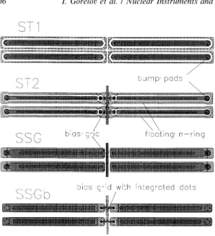
+implant dot near each pixel. When voltage is applied to the grid, it reaches each pixel by punchthrough from its corresponding dot. Variations to this design are termed ‘‘small dot grid’’ (SMD), and ‘‘large dot grid’’ (LAD), for dot diameters of 10 and 15 mm, respectively, and the ‘‘no dot grid’’ (NOD), in which the dot is eliminated and the bias reaches the implant directly from the neighboring bus line.
Figs. 1, 2 and 3 illustrate the SMD, LAD, and NOD designs, respectively.
Two p-spray technology options were examined:
standard and moderated. These are distinguished
by the p-type dopant density profile. For a wafer
with standard p-spray, the entire surface has a uniform implantation dose of 3.5 10
12cm
2of p- type implant. In moderated p-spray, the concen- tration varies from 1.5 10
12cm
2at the inter-
faces with the n
+implants to 3.5 10
12cm
2in the center of the gaps between pixels. Fig. 4 illustrates standard and moderated p-spray and p-stop isolation.
The density of standard p-spray, and the maximum density of moderated p-spray, are slightly higher than the observed saturation value (3 10
12cm
2) of surface charge density and so maintain isolation throughout the radiation life- time of the sensor. The lower density at the n–p interfaces in moderated p-spray reduces both the capacitance between implants and the electric field at the interfaces.
The moderated design consequently has the property that, prior to irradiation, it provides higher breakdown voltage than does a comparable design in standard p-spray. As irradiation pro- ceeds, the breakdown voltage rises just as in the case of normal p-spray. After being irradiated to the same fluence, a standard and a moderated p- spray device show the same leakage current versus bias voltage characteristic.
The tolerance of silicon devices to radiation can be improved by deliberately introducing oxygen to the substrate [6]. Oxygenated wafers with concen- trations ranging from 2 10
17to 4 10
17cm
3were examined. The oxygen enhancement was
Fig. 1. The SMD bias grid design.
Fig. 2. The LAD bias grid design.
Fig. 3. The NOD bias grid design.
achieved by a 24 h diffusion at 1150 1 C after the oxidation prior to processing.
2. Characteristics of the prototypes
Table 1 summarizes many of the features of the prototypes. Prototype 1a wafers included two tiles and 17 single-chip sensors. The details of the Prototype 1a design were described thoroughly elsewhere [1] and are not all repeated here. The basic cell size was 50 mm 400 mm. One of the tiles (Tile 1) and three of the single chips (ST1) had the same design and examined p-stop technology. The other tile (Tile 2) and three of the single chips (ST2) had a different design and examined p-spray technology. The remainder examined other geo-
metrical options, including one called SSG, that used the p-spray technology and had no n
+atoll surrounding the pixel (see below). This design eventually evolved into the ATLAS production sensor design (Tile 3). Fig. 5 shows the features of the ST1, ST2, and SSG devices. Prototype 1a wafers were fabricated by three companies: CiS (16 non-oxygenated wafers), Seiko (20 non-oxyge- nated wafers), and TESLA (nine oxygenated wafers and seven non-oxygenated wafers). The thickness of the wafers was 300 mm for Seiko, 280 mm for CiS, and 280 mm for TESLA. The crystal orientation was / 1 1 1 S for CiS, / 1 0 0 S for Seiko, and / 1 1 1 S for TESLA. Of the CiS wafers, 13 had Si
3N
4passivation and three, SiON passivation. All of the Seiko and TESLA wafers were passivated with Si
3N
4. In the figures of this
Fig. 4. Isolation techniques, from left to right: p-stop, standard p-spray, and moderated p-spray.
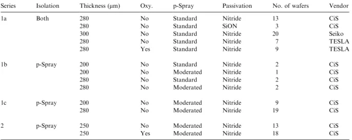
Table 1
Characteristics of the ATLAS prototype pixel sensor wafers
Series Isolation Thickness (mm) Oxy. p-Spray Passivation No. of wafers Vendor
1a Both 280 No Standard Nitride 13 CiS
280 No Standard SiON 3 CiS
300 No Standard Nitride 20 Seiko
280 No Standard Nitride 7 TESLA
280 Yes Standard Nitride 9 TESLA
1b p-Spray 200 No Standard Nitride 2 CiS
200 No Moderated Nitride 1 CiS
280 No Standard Nitride 2 CiS
280 No Moderated Nitride 2 CiS
1c p-Spray 200 No Moderated Nitride 9 CiS
280 No Moderated Nitride 19 CiS
2 p-Spray 250 No Moderated Nitride 13 CiS
250 Yes Moderated Nitride 18 CiS
paper, Seiko is indicated as ‘‘Vendor 1’’, CiS as
‘‘Vendor 2’’, and TESLA as ‘‘Vendor 3’’. Ref. [1, Fig. 2] shows the Prototype 1a wafer.
Prototype 1b wafers were fabricated with standard silicon and included one functional tile and 17 single-chip sensors, all with p-spray isolation. As we have reported elsewhere [1], the layout of Prototype 1a p-spray sensors produced a charge collection problem associated with the n
+atoll surrounding the pixel. In Prototype 1b the atoll was eliminated and the width of the pixel implant was slightly increased. Modifications were made in the bias grid as well to reduce some residual charge loss: whereas the bias lines of Prototype 1a had been implanted, the bias lines of Prototype 1b were metalized, with only the bias dot implanted. The bias dot was integrated with the primary n
+implantation for its cell.
The single-chip devices in Prototype 1b used the same geometries as Prototype 1a versions with the exception of the design change mentioned; their names were correspondingly modified to SSGb, etc. Fig. 5 shows the features of the SSGb devices.
Relative to SSG, their dimensions in the short direction are changed from 37 mm+13 mm (gap) to 30 mm+20 mm (gap). Prototype 1b wafers used the same design for their tiles (called Tile 3) as for the SSGb single-chip sensor. The 1b prototypes
examined two thicknesses, 200 and 280 mm. Some sensors of each thickness used moderated p-spray while some used standard: of the four 280 mm wafers, two were standard p-spray and two were moderated. Of the three 200 mm wafers, two were standard p-spray and one was moderated. All seven Prototype 1b wafers were manufactured by CiS and used Si
3N
4passivation and / 1 1 1 S crystal orientation.
Prototype 1c wafers were geometrically similar to Prototype 1b wafers except for a revision in the dimensions of the contract openings in the oxide layer between the metal layer and the n
+implant.
The opening had been rectangular, of dimensions 306 mm 12 mm, in Prototype 1b. In Prototype 1c the structure was revised to four circular openings of diameter 13.5 mm each. The revision was made to decrease the area of unprotected implant.
Prototype 1c used standard silicon, Si
3N
4passiva- tion, / 1 1 1 S crystal orientation, and moderated p-spray for all structures. CiS fabricated all Prototype 1c wafers. Nine wafers of thickness 200 mm and 19 wafers of thickness 280 mm were examined. Data from Prototypes 1b and 1c have been combined in the figures in this paper. (In cases where this is done, the devices are referred to as, for example, ‘‘SSGb/c’’.)
Three tiles and 12 single chips were included on each Prototype 2 wafer to test the SMD, LAD, and NOD bias grid designs. To allow a compar- ison, devices were fabricated with oxygenated and non-oxygenated substrates. All of the wafers were fabricated with moderated p-spray and the / 1 1 1 S crystal orientation, passivated with silicon nitride. The wafers were 250 mm thick. Prototype 2 wafers were fabricated by CiS (18 oxygenated wafers and 13 non-oxygenated ones).
The final design selected for the ATLAS production sensors uses p-spray isolation and the SMD bias grid on oxygenated wafers of thickness 250 mm. (The SMD, SSGb/c, and Tile 3 bias grids are identical). The pixel cells have dimensions 50 mm 400 mm, the reduced-size oxide layer open- ings, / 1 1 1 S crystal orientation, and Si
3N
4passivation. Each pixel consists of one rectangular n
+implantation of dimensions 30 mm 382.5 mm.
The gap between two adjacent pixels is 20 mm in the short-pitch direction, 15 mm in the long-pitch
Fig. 5. The ST1, ST2, SSG, and SSGb designs.
direction at the pixel side with the bump pad, and 20 mm at the other pixel side, where the bias grid is located. The bias grid connection to each pixel is provided using a round n
+implant integrated in the n
+-pixel implant with 10 mm diameter and 5 mm gap. The minimum-sized gap minimizes the punch-through voltage. The width of the pixel implant crossed by the metal line (also 5 mm) is minimized to limit the coupling. The bias dots of all pixels in an adjacent pair of columns are connected via a metal line to an outer n
+implantation which surrounds the border of the active sensor area.
3. Irradiation conditions
A subset of the prototypes was irradiated with different fluences to simulate the ATLAS environ- ment. Irradiations were performed with the 55 MeV proton beam at Lawrence Berkeley Na- tional Laboratory, USA. Unless otherwise noted, all fluences are quoted in 1 MeV neutron equiva- lent, designated as 1-MeV n
eq: Irradiations were made at room temperature without bias. Storage and subsequent measurements were done at or below 10 1 C to inhibit annealing of bulk damage.
Quoted currents have been normalized to 10 1 C according to the equation IðTÞ p ðkT Þ
2e
E=2kBT; where k
Bis Boltzmann’s constant and E ¼ 1:21 eV is the activation energy.
4. Measurements and requirements 4.1. Introduction
The techniques by which the measurements were made have been described previously [1,2]. Ref. [1, Fig. 10] shows the setup for measurements of leakage current versus bias voltage (‘‘I–V’’). Two probe needles are placed on the p-side, one on the active area and another at the wafer edge or device scribe line. The contact to the edge or scribe line is shorted to the n-side. The breakdown voltage is defined as the highest measured voltage for which the normalized leakage current is o 1 mA for tiles and o 100 nA for single chips. ATLAS requires the
breakdown voltage of the unirradiated sensors to be >150 V or V
depletionþ 50 V, whichever is higher.
V
depletionis required to be p 120 V. In this paper, because the distinction is small, we simply require V
breakdown> 150 V. For all voltage measurements reported in this paper, the uncertainty on the central value is 75 V.
Charge collection and spatial resolution were measured at the CERN SPS accelerator with a pion beam of 180 GeV/c momentum. A beam telescope consisting of four pairs of silicon micro- strip detectors (each with two planes of orthogonal strips) was used to measure the transverse position of the incident beam particles. The position resolution of tracks projected onto the test devices varied from 3.0 to 6.0 mm depending upon the telescope configuration. The sensors were inte- grated in modules with prototype ATLAS electro- nics chips, which operate with a 40 MHz clocking rate and measure pulse height by recording the time that the amplifier remains above the thresh- old. Typical thresholds were about 3000 electrons, and threshold dispersion was 170 electrons rms.
The noise was typically 150 electrons rms. Resolu- tions were measured for both analog and digital clustering algorithms [2] as a function of track incidence angle. The charge collected by the pixels was studied as a function of the point of impact of the traversing particles relative to a pair of pixel cells. For hits not at a pixel center, the signal was shared between several pixels, and the sum of the pixel measurements is reported. The electronics threshold was set at 2000 electrons for the charge- sharing studies. During test beam runs, unirra- diated sensors were operated at 150 V and irradiated ones at 600 V (unless otherwise stated).
4.2. Isolation: p-stop versus p-spray
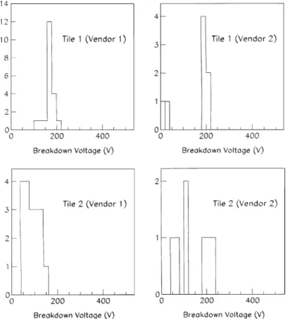
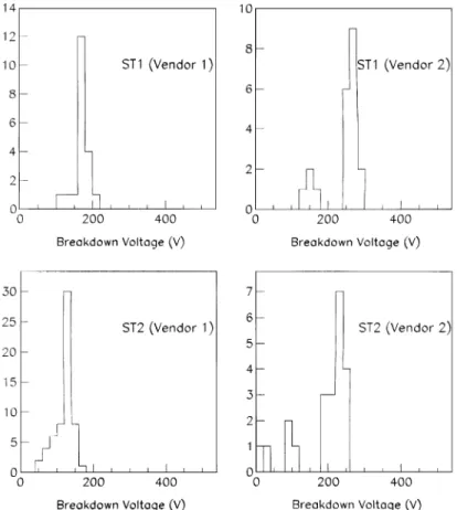
Figs. 6 and 7 show the breakdown voltages of devices of the Tile 1 (p-stop) and Tile 2 (p-spray) designs for unirradiated tiles and single-chip sensors, respectively. One sees that in a low- radiation environment, the two designs show comparable breakdown voltage, with the Tile 1/
ST1 being potentially slightly better. The decision
between p-stop and p-spray isolation is, conse-
quently, highly linked to the fluence expected.
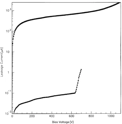
Figs. 8 and 9 show I–V curves for ST1- and ST2- type single-chip sensors, respectively, that have been irradiated to the same fluence (2.5 10
1455- MeV p/cm
2, equivalent to 4.3 10
141-MeV n/
cm
2), measured at 20 1 C (measurement normal- ized to 10 1 C), and are otherwise identical in fabrication and handling. One sees that whereas the ST1 breaks down at approximately 150 V (the exact value is not well defined, but is somewhat dependent on the sensor geometry, due to the absence of a bias grid structure), the ST2 remains viable up to at least 500 V. This radiation resistance of p-spray motivated the selection of that technology for future prototype cycles.
4.3. Passivation
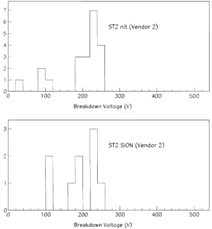
Fig. 10 compares the breakdown voltages of ST2 sensors with nitride and SiON passivation.
Both types behave acceptably, showing compar- able breakdown voltages. Both could be compa- tible with bump bonding processes. Nitride was selected by ATLAS.
4.4. Geometrical options using p-spray isolation
Fig. 11 shows the average collected charge as a function of the position of the perpendicularly incident track on the cell in the short dimension, for ST1, ST2, and SSG sensors. Fig. 12 shows the average collected charge as a function of the position of the perpendicularly incident track relative to a pair of pixels in the long dimension, for ST1, ST2, and SSG. Charge loss in ST2 was approximately 25% over the full cell. A 20% loss is attributed to the presence of the floating n-ring in the design. The remaining 5% loss is due to the implanted bias grid. The SSG and ST1 designs had
Fig. 6. The breakdown voltages of unirradiated nitride-passivated Prototype 1 tiles of types Tile 1 and Tile 2.
Fig. 7. The breakdown voltages of unirradiated nitride-passivated Prototype 1 single-chip sensors of types ST1 and ST2.
Fig. 8. Current versus voltage of an ST1 single-chip sensor fabricated by CiS, normalized to101C, after irradiation with 2.51014 55-MeV p/cm2.
Fig. 9. Current versus voltage of an ST2 single-chip sensor with standard p-spray, fabricated by CiS, normalized to101C, after irradiation with 2.5101455-MeV p/cm2.
Fig. 10. The breakdown voltages of unirradiated nitride-passivated Prototype 1 single-chip sensors of types ST2 with nitride and SiON passivation.
good charge collection performance over the full cell except for minor local losses not exceeding 10% locally and not significantly affecting the average over the full cell. The approximately 10%
local loss in the SSG design is similarly associated with its bias grid—in this case the dot structure.
The 10% local loss in the ST1 is due to the fact
that the gap between p-stops in that design acts (due to electron accumulation) like a small n
+region. On the basis of these results, the SSG design was chosen over the ST2.
Table 2, which uses information taken from Ref.
[2], summarizes measured spatial resolution for unirradiated ST1, ST2, SSG, and SSGb. As is
Fig. 11. The average collected charge as a function of the position within a pixel cell of short dimension 50mm, for ST1, ST2, and SSG sensors. The total charge of the clusters is shown in units of thousands of electrons.
Fig. 12. The average collected charge as a function of the position relative to a pair of pixel cells of long dimension 2400mm, for ST1, ST2, and SSG sensors. The total charge of the clusters is shown in units of thousands of electrons.
Table 2
Spatial resolution of unirradiated detectors
Design ST1 ST2 SSG SSGb
Thickness (mm) 280 280 280 200
At normal incidence:
Charge sharing region (mm) 13.6 9.2 14.0 6.2
Digital resolution (mm) 10.7 12.1 10.5 12.7
Analog resolution (mm) 10.4 12.0 10.1 12.6
Best analog resolution (mm) 5.3 6.5 5.8 6.2
Corresponding incidence angle (deg.) 10 10 10 15
The data were taken with sensors biased to 150 V. The telescope extrapolation uncertainty has not been subtracted. The statistical uncertainties on the measurements of spatial resolution and charge sharing region are of the order of 0.3mm.
Table 3
Spatial resolution and depletion depth of ST2 detectors for several fluences and of a highly irradiated SMD detector
ST2 SMD
Fluence (n/cm2) 0 51014 1015 1015
At normal incidence:
Charge sharing region (mm) 9.2 5.8 3.5 4.3
Digital resolution (mm) 12.1 13.1 13.7 12.5
Analog resolution (mm) 12.0 12.9 13.7 12.4
Best analog resolution (mm) 6.5 7.3 9 7.4
Corresponding incidence angle (deg.) 10 10 15 15
Depletion depth (mm) 280710 26178 20379 230
The data were taken with irradiated sensors biased to 600 V and unirradiated sensors biased to 150 V. The telescope extrapolation uncertainty has not been subtracted. The statistical uncertainties on the measurements of spatial resolution and charge sharing region are of the order of 0.3mm.
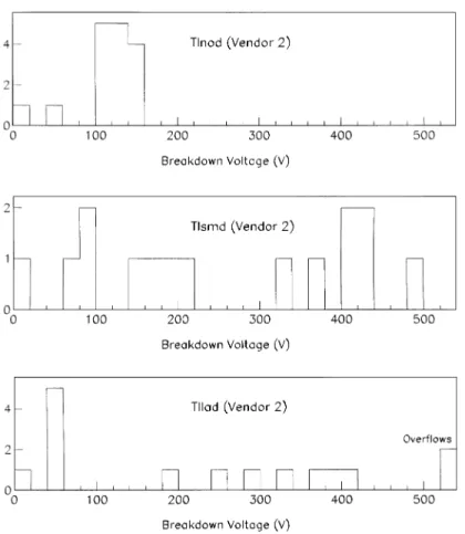
Fig. 13. The breakdown voltages of unirradiated tiles of type NOD, SMD, and LAD.
discussed in Ref. [2], the statistical uncertainties on the measurements of spatial resolution and charge- sharing region in Tables 2 and 3 are of the order of 0.3 mm, and the telescope extrapolation uncer- tainty (between 3 and 6 mm) has not been subtracted. The superior performance of the SSG and ST1 designs relative to the ST2 design is due to their negligible charge loss, allowing them to have a larger charge-sharing region and better spatial resolution. The SSGb sensor included in Table 2 also showed negligible charge loss. Its smaller thickness (200 mm) accounts for its slightly worse resolution for perpendicular incidence, its reduced charge-sharing region, and the larger angle at which its best spatial resolution is reached.
One sees that all of the proposed designs provide good resolution, so the decision among them can be based upon other features, including charge- collection efficiency.
Table 3, which uses information taken from Ref.
[2], summarizes measured spatial resolution and depletion depth for ST2 with three levels of radiation damage and SMD with high radiation damage. All of the data in this table were taken with irradiated sensors biased to 600 V and unirradiated sensors biased to 150 V. One sees that the resolution of a p-spray device remains consistent with ATLAS needs throughout the full expected radiation lifetime.
Tile 3 devices incorporate the improved SSGb bias grid and so address the charge-collection problem present with ST2 devices. On standard substrates with standard p-spray, the good break- down voltage characteristic demonstrated by Tile 2 devices is maintained in Tile 3.
Fig. 13 compares the breakdown voltages of tiles with the SMD, LAD, and NOD bias grid designs. All of the devices in the figure were
Fig. 14. Leakage current versus bias voltage of an SSG-type single-chip sensor fabricated with moderated p-spray, normalized to 201C, before (lower curve) and after (upper curve) irradiation to a fluence of 1.6101455-MeV p/cm2.
fabricated with moderated p-spray on oxygenated wafers (see below). One sees that the SMD and LAD yield the same fraction of devices with acceptable breakdown voltage—approximately 75%—while the NOD does not, in general, meet the breakdown voltage requirement. As the SMD and LAD are equivalent in this regard, SMD was selected because the smaller dot leads to slightly lower charge loss in the region of the bias dot.
Table 3 summarizes measured charge sharing and spatial resolution information as well as depletion depth for an SMD design sensor at fluence 10
15n/cm
2. The sensor tested included all of the options ultimately included in the ATLAS baseline; performance superior to that obtained by ST2 designs irradiated to the same fluence is due to the improved charge collection and fuller depletion achieved. One sees that the resolution for this
design remains excellent at the maximum fluence required for the ATLAS design.
4.5. Moderated versus standard p-spray
Fig. 14 shows the current–voltage characteristic of the same moderated p-spray sensor before and after irradiation to a fluence of 1.6 10
1455-MeV p/cm
2(2.7 10
141-MeV n
eq/cm
2) and normal- ization to the effective current at 20 1 C. The principal feature to notice is the increase in breakdown voltage with fluence, from about 580 V to well above 800 V.
Figs. 15 and 16 in this section compare the breakdown voltage characteristics of devices fab- ricated with moderated p-spray and with standard p-spray. The figures reflect results from single chip SSGb/c and Tile 3 devices. One sees that pre-
Fig. 15. The breakdown voltages of unirradiated tiles of type SSGb/c with standard (upper figure) and moderated (lower figure) p- spray.
irradiation breakdown voltage is significantly improved by the moderated p-spray, which per- mits pre-irradiation breakdown voltages in excess of 300 V to be attained.
4.6. Oxygenated versus non-oxygenated substrate
The advantage of oxygenated substrates has been demonstrated in measurements both in the laboratory and in the test beam.
The laboratory procedure measures the deple- tion voltage of silicon sensors bump-bonded to electronics chips. The method uses a g-ray source and measures the interaction rate in the sensor as a function of the bias voltage. Fig. 17 shows the setup for the measurement: the g source irradiates the p-side of a single-chip sensor integrated with a prototype ATLAS electronics chip. During the
measurements the device and the source are maintained at about 5 1 C.
The interaction rate produced in the sensor by the 60 keV photons of a sealed
241Am source is
Fig. 16. The breakdown voltages of unirradiated tiles of type Tile 3 with standard (upper figure) and moderated (lower figure) p-spray.
Fig. 17. The setup for laboratory measurements of depletion voltage of pixel sensors bump bonded to electronics.
related to the sensor sensitive volume, which is a function of the bias voltage. It is given by the hitbus signal, which is a fastOR of the 18 164 pixel matrix. Through a completely automated program, a bias voltage scan is performed, and at each step several measurements of the hitbus frequency are taken. The mean of these measure- ments is plotted, yielding a function which rises at low voltages and is flat at high voltages (for which the sensor is overdepleted). Lines with different slopes are fitted to the two regions of this function, and the intersection point of the lines is taken as an estimate of the depletion voltage. We refer to this as the plateau voltage.
For irradiated sensors, the details of the flip- chipping process must be monitored carefully, as the readout chip is connected to the sensor after the sensor has been irradiated. The heat involved accelerates the effect of the radiation damage in the sensor. Fig. 18 shows the hitbus frequency versus bias voltage for interactions produced with an
241Am source in three sensors with the same
temperature history. Two of the sensors were fabricated with oxygenated silicon while the third used standard silicon. All three were irradiated to the same fluence, 3.0 10
14cm
2. The oxygenated sensors have very similar interaction rate char- acteristics, showing a plateau voltage of about 100 V. The non-oxygenated sensor has a higher plateau voltage, about 150 V.
Fig. 19 shows the hitbus frequency versus bias voltage for interactions produced with an
241Am source in three oxygenated sensors irradiated to different fluences. The temperature history for the three sensors is the same. The plateau voltages obtained are 150, 180, 280 V for fluences of 3.0 10
14, 5 10
14and 1.1 10
15cm
2, respec- tively. The measured values are consistent with predictions using damage parameters in a model [6] that considers the received particle flux and the temperature history from irradiation to the time of measurement.
The depletion depth has also been studied in test beam experiments at CERN using the method of
Fig. 18. The interaction rate versus bias voltage for three pixel sensors irradiated to 3.01014cm2. The upper two use oxygenated silicon while the lower uses standard.
Fig. 19. The interaction rate versus bias voltage for pixel sensors fabricated with oxygenated silicon and irradiated to 3.01014 (upper), 51014 (middle), and 1.11015cm2 (lower). The plateau voltage obtained by the fit is shown for each plot.
inclined tracks [2]. Data were taken with a particle beam incident on the sensor at angles of 20 1 and 30 1 with respect to the normal to the pixel plane.
The maximum depth of the track segment subtended by the hit pixels was measured at various bias voltages. The results are summarized in Table 4. In some cases [7] only lower limits on depletion depths could be obtained. Table 4 shows that oxygenated sensors have larger depletion depths than non-oxygenated sensors irradiated to the same fluence and operated at the same bias voltage. For example, after a fluence of 10
15cm
2, a sensor made with oxygenated substrate and operated at 400 V has the same depletion depth as one made with standard substrate operated at 600 V. Furthermore, after a fluence of 0.5 10
15cm
2, a 250 mm thick sensor made with oxygenated substrate is almost fully depleted at 250 V, while a non-oxygenated sensor requires 400 V to attain a depth of 250 mm.
5. Conclusions
Prototype sensors for the ATLAS silicon pixel detector have been electrically characterized. The current and voltage characteristics, charge-collec- tion efficiencies, and resolutions have been exam- ined. Devices were fabricated on oxygenated and standard detector-grade silicon wafers. Results are presented from prototypes which examine p-stop and standard and moderated p-spray isolation for
a variety of geometrical options. The response of the devices to fluences relevant to LHC operation is examined. The final design selected for ATLAS uses moderated p-spray isolation and the SMD bias grid on oxygenated wafers of thickness 250 mm. The pixel cells have dimensions 50 mm 400 mm, Si
3N
4passivation, and / 1 1 1 S crystal orientation. Additional detailed geometri- cal choices have also been described.
Acknowledgements
The collaboration thanks P. McMahan and the operating staff of the 88 inch cyclotron at Lawrence Berkeley National Laboratory for assis- tance with the proton irradiation.
References
[1] M.S. Alam, et al., Nucl. Instr. and Meth. A 456 (2001) 217.
[2] I. Gorelov, et al., Nucl. Instr. and Meth. A 481 (2002) 204.
[3] ATLAS Pixel Detector Community, ATLAS pixel detector technical design report, CERN/LHCC/98-13, 1998.
[4] G. Batignani, et al., Nucl. Instr. and Meth. A 277 (1989) 147.
[5] R.H. Richter, et al., Nucl. Instr. and Meth. A 377 (1996) 412.
[6] The ROSECollaboration, Third RD48 status report, CERN/LHCC 2000-009, 2000.
[7] T. Lari, Study of silicon pixel sensors for the ATLAS detector. Ph.D. Thesis, University of Milano, October 2001.
Table 4
Depletion depth of irradiated pixel sensors as measured in a test beam
Fluence (n/cm2) Oxygenated Thickness (mm) Bias voltage (V) Depletion depth (mm)
0.51015 No 280 400 252710
0.51015 No 280 200 14777
0.51015 Yes 250 400 >24278
0.51015 Yes 250 250 >230714
0.51015 Yes 250 200 >184713
1.01015 No 280 600 20379
1.01015 No 280 300 111710
1.01015 Yes 250 600 >22778
1.01015 Yes 250 430 >225714
1.01015 Yes 250 400 >201712