1
Direct determination of spin–orbit interaction coefficients and realization of the persistent spin helix symmetry
A. Sasaki1, S. Nonaka1, Y. Kunihashi1, M. Kohda1, T. Bauernfeind2, T. Dollinger2, K. Richter2 and J. Nitta1*
1Graduate school of Engineering, Tohoku University, 6-6-02 Aramaki-Aza Aoba, Aoba-ku, Sendai 980-8579, Japan
2Institut für Theoretische Physik, Universität Regensburg, 93040 Regensburg, Germany
*Correspondence to: nitta@material.tohoku.ac.jp
2
Spin-orbit interaction (SOI) plays a crucial role in device fields from physics to applications, such as Majorana Fermions, topological insulators, quantum information and spintronics to name only a few. Two types of SOIs, the Rashba SOIand the Dresselhaus SOI, act on spins as effective magnetic fields with different directions.
Although spin angular momentum is not a good quantum number in spin-orbit coupled systems, spin SU(2) symmetry is preserved and the so-called persistent spin helix state is realized when isequal to . Existing methods to evaluate / require fitting analyses that often include an ambiguity in the parameters used. Here, we experimentally demonstrate simple and fitting parameter-free techniques to determine / and to deduce the absolute values of and by detecting the effective magnetic field direction and the strength induced by the two SOIs. Moreover, we observe the spin SU(2) symmetry by gate tuning.
3
As an essential feature of spin-orbit interaction (SOI), the spin of an electron moving in an electric field experiences, in its rest frame, an effective magnetic field that couples to the spin’s magnetic moment, even in the absence of any external magnetic field. So, the SOI is ubiquitous and appears in many different areas from physics to applications1-3. The SOI can be engineered by material design or by tuning an electric field4,5 to explore new spin-related phenomena and spin functionalities. In semiconductor-based spintronics, for example, this effective magnetic field Beff can be used for generation6, manipulation7-12, and detection13 of spins solely by electrical means. However, the SOI inevitably gives rise to spin relaxation14, thus disrupting long spin coherence. This crucial problem can be overcome by employing two different types of SOIs; the Rashba15 and the Dresselhaus16 SOIs. Spin SU(2) symmetry is realized and spin relaxation is suppressed correspondingly when both SOIs are of equal strength, giving rise to the persistent spin helix (PSH) state17-20. As a result, precise evaluation and control of / ( and denote the strengths of Rashba and Dresselhaus SOIs, respectively) pave the way for future applications in spintronics and quantum information21-23. However, for transport measurements, simultaneous evaluation of Rashba and Dresselhaus SOIs usually involves large ambiguities due to model-dependent fitting24, and in optical measurements25,26, fitting analyses are also required. Consequently, there has been the quest for a simple, robust and reliable technology for evaluating / for a long time. Here, we demonstrate a fitting-free determination of in-situ / in transport measurements under the coexistence of Rashba and Dresselhaus SOIs. In narrow wires, application of an in-plane magnetic field Bin modulates the amplitude of the magneto-conductance, i.e. weak localization (WL) through additional dephasing arising from spin-induced time reversal symmetry breaking27. Theory predicts the maximum amplitude of WL when Bin and Beff are parallel28. This enables us to evaluate / from the anisotropic WL amplitude, without
4
relying on any fitting. By applying the proposed concept to InGaAs based wire structures, we realize the gate controlled PSH state and find a novel finger print of the PSH state. In addition to the evaluation of the ratio /, the absolute values of and can be deduced from the minimum WL amplitude when Bin and Beff have equal strengths. Our demonstration of proposed metrological concept28 can be applied to a wide range of materials, since the direction and the strength of the effective magnetic fields in a confined structure are directly related to and . As a proof of concept we provide measurements in InGaAs wires. The precise determination of and is indispensable to explore new spin-related phenomena and functionalities.
5
According to the proposed metrological concept28, Evaluation of / is achieved by detecting eff of Beff = BR + BD direction, where BR and BD are the effective magnetic fields induced by the Rashba and linear Dresselhaus SOIs. For a quantum well grown in the [001]
direction of III–V zinc-blende semiconductor heterostructures, The corresponding Hamiltonians are given by
x y y x
R p p
H
, (1)
x x y y
D p p
H
, (2)
where and are coefficients of the Rashba and Dresselhaus SOIs, which determine the strengths of BR and BD, respectively. In equations (1,2) i and pi (i = x, y) are the Pauli spin matrices and the electron momentum. The x and y directions are parallel to [100] and [010], respectively. Let us assume a one dimensional (1D) wire along [100], since electron momentum is restricted to ±p along the wire direction. The direction of Beff acting on electron spins is fixed as uniaxial29,30. Owing to the perpendicular orientation of BR and BD, the relationship between the SOI parameters and the effective field orientation eff is simply given by
taneff
. (3)
It should be noted that the cubic Dresselhaus SOI vanishes along the [100] axis. Hence, by the detection of eff in the 1D wire, direct evaluation of the / ratio is possible.
The central concept to determine eff through transport measurements is schematically shown in Fig. 1. For a narrow wire with W << Lso (W is the wire width and Lso is the spin precession length. Lso = 2/2m or 2/2m , where m is an effective mass), theory predicts that the narrow wire can be treated as quasi-one dimensional, and the Beff direction becomes uniaxial (green arrows in Fig. 1)28. Since the randomization of the spin precession axes is suppressed due to the one dimensional confinement of electron momentum p, the spin
6
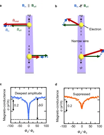
Figure 1: WL anisotropy to the relative angle between Beff and Bin. In the upper panels a,b, the directions of total magnetic field Btotal = Bin + Beff are shown for ± p momentum directions.
In the lower panels c,d, calculated WLs are shown at /= 2/3 in a [100] wire with |Bin| = 0.75 T for Bin || Beff (c: in = 146º) and Bin ∦ Beff (d: in = 25º), where in is the angle of in-plane magnetic field defined with respect to the [100] direction. The magneto-conductance is plotted against the magnetic flux in a unit cell of the numerical grid Φs = a2|Bp| (a is the lattice constant and Bp is the perpendicular magnetic field) in units of the magnetic flux quantum Φ0 = h/e. a,c When Bin || Beff, the total magnetic field Btotal along the ± p directions remains uniaxial showing the deepest WL amplitude. b,d, When Bin ∦ Beff, Btotal is randomized for ± p electron directions, suppressing the WL amplitude.
relaxation length is enhanced in a narrow wire and the magneto-conductance exhibits weak localization (WL), predicted theoretically29,30 and confirmed experimentally31,32. The application of a static in-plane magnetic field Bin further induces the additional spin relaxation by breaking the uniaxial alignment of Beff. The additional spin relaxation induces dephasing in the time-reversal related pairs of electron paths by mixing spin up and down phases i.e.
Bin Beff Btotal
Electron
Narrow wire
Bin || Beff Bin || Beff
Deepest amplitude Suppressed
Φs/ Φ0
0.2 +p
-p
ΔG
a b
c d
-p +p
0.2
Φs/ Φ0 Magneto-conductance σ (e2/h)
Magneto-conductance σ (e2/h)
0 50
-50
-100 100 -100 -50 0 50 100
7
spin-induced time-reversal symmetry breaking27. This dephasing leads to weaker quantum interference, resulting in suppression of the WL amplitudes. When Bin is applied in parallel to Beff (Fig. 1a), the total magnetic field Btotal = Bin + Beff for ± p directions is still uniaxial, preserving the long spin relaxation length. However, when Bin is no longer parallel to Beff (Fig.
1b), the direction of Btotal is different for ± p momenta, enhancing the additional spin relaxation.
Since the electron dephasing induced by the spin relaxation process decreases the amplitude of WL, the WL amplitude becomes anisotropic as a function of the relative angle between Bin and Beff (Fig. 1c and 1d). This concept enables us to determine eff by tilting the direction of Bin, and therefore, to determine the / ratio by using the relation of equation (3) without any fittings.
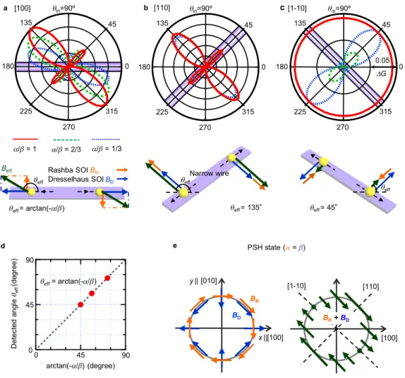
In order to confirm the concept presented above, we conduct numerical calculations of the magneto-conductance of wires with different/ values including the persistent spin helix (PSH) configuration. In this calculation, we include also results for wires oriented along the [110] and [1-10] directions and compare our results with the data for the wire in [100] direction, since wires along [110] and [1-10] provide parallel and anti-parallel configurations between BR
and BD,respectively. We conduct the numerical calculations based on the recursive Green’s function approach28 (for details, see supplementary information). We theoretically calculate the magneto-conductance of a narrow wire by changing the perpendicular magnetic field Bp under the fixed in-plane magnetic field Bin whose angle in is defined with respect to the [100]
direction. Three different wire directions are examined along the [100], [110] and [1-10] axes, and are referred to as [100], [110] and [1-10] wire, respectively. It should be noted that the wire width is set to 20 nm, which does not give rise to a purely 1D confinement, but is smaller than the spin precession length. Figures 1c and 1d show the calculated results for the [100] wire at in
= 25º and 146º (Bin = 0.75 T), exhibiting clear WL signals with different conductance amplitude.
We define the amplitude of WL as G (Fig. 1c) and produce a polar-plot as a function of in for different / ratio and wire directions (Figs. 2a – 2c). The WL amplitude shows two-fold
8
Figure 2: Numerical results of conductance in quasi-one dimensional quantum wires. The calculation is performed for W << Lso without cubic Dresselhaus SOI. We fix the ratio / at 1/3 (blue dotted line), 2/3 (green dashed line) and 1 (red solid line). a,b,c, polar-plots of WL amplitudes as a function of in along [100], [110] and [1-10] directions. Schematic insets indicate the angles of effective magnetic field eff for each wire orientation. d. Detected eff was perfectly fitted in accordance with relation eff = arctan(-/). e. Orientation of Beff in momentum space under the persistent spin helix state (PSH state: = ). The arrows indicate the direction of the effective magnetic field Beff describing spin-orbit coupling. The length of the shown arrows indicates the strength of Beff. In the left panel, Rashba and Dresselhaus effective magnetic fields (BR and BD respectively) are shown. In the right panel, total effective magnetic field Beff = BR + BD is shown. The PSH state induces uniaxial alignment of Beff.
symmetries for all wire directions. Furthermore, its symmetry axis depends on the crystal direction. Such dependences are understood in terms of the relative angle between Bin and Beff.
BR+BD
b c
[100] [110] [1-10]
a
180 0
270
45
225 315
135
180 0
270
45
225 315
135
180 0
270
45
225 315
135
in=90º in=90º in=90º
/= 1 /= 2/3 /= 1/3
eff
Rashba SOI Dresselhaus SOI
eff= arctan(-/) BR
BD effNarrow wire
eff= 135°
eff
eff= 45°
e PSH state (=)
BR BD
[1-10] [110]
y|| [010]
x||[100]
d
arctan(-/) (degree) Detected angleeff(degree)
0 45 90
0 45 90
eff= arctan(-/)
[100]
0.05
G
Beff
9
Since the Bin || Beff configuration does not enhance the spin relaxation, the angle of the maximum WL amplitude corresponds to the Beff direction. On the other hand, the Bin ∦ Beff
configuration induces spin relaxation resulting in a reduced WL amplitude. For [110] and [1-10] wires, since Beff appears always along 135º and 45º directions, respectively, the WL amplitude becomes maximal at in = 135º and at 45º, and is thus unaffected by the different /
ratio (Fig. 2b and 2c). For the [100] wire, however, the Beff direction changes with the / ratio, resulting in the angular shift of the maximum WL amplitude (Fig. 2a). As shown in Fig. 2d, the angle of the maximum WL amplitude (eff) is perfectly aligned to equation (3). In the PSH state, i.e., at / = 1 (red plot in Fig. 2a – c), while the maximum WL peak still appears at in = 135º for the [110] wire, interestingly, the anisotropy of the WL amplitude is quenched for the [1-10]
wire. This is due to the mutual compensation of BR and BD (Fig. 2e). This numerically observed quench of the WL anisotropy is a finger print for the PSH states.
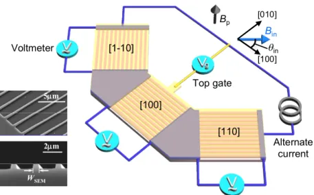
In order to utilize this concept in a real device, we fabricate parallel wire structures based on InGaAs, as shown in Fig. 3 (more information on the device structure and fabrication is found in Methods). An n-In0.52Al0.48As / 10 nm In0.7Ga0.3As / n-In0.52Al0.48As quantum well is designed to minimize the Rashba SOI to values of the same order as the Dresselhaus SOI by Si doping in both In0.52Al0.48As barriers. We prepare parallel wires along the [100], [110], and [1-10] directions in series (Fig. 3) and cover the entire structure with an Al2O3 / Cr / Au top gate electrode to control through the gate voltage (Vg). The wire width of 750 nm is set to be shorter than the spin precession length Lso = 2/2m 1.79 m at carrier density Ns = 2.0×1012 cm-2 in the InGaAs 2DEG (two dimensional electron gas) channel. Ns and electron mobility at Vg = 0 V are 2.44×1012 cm-2 and 6.68 m2/Vs, respectively. The magneto-conductance measurement is simultaneously performed for three wire directions by sweeping Bp under the constant Bin and Vg at T = 1.7 K.
10
Figure 3: Schematic illustration of measurement configuration.
The shown setup allows us to simultaneously perform conductance measurements in all of the three considered wire orientations along the [100], [110] and [1-10] axes, respectively. The conductance for each wire orientation is an average over multiple wires in order to minimize signatures from the universal conductance corrections. The scanning electron microscope (SEM) images at the lower left are the example of InGaAs wire structure. Each image shows top view (upper picture) and side view (lower picture), respectively.
Figure 4a shows the magneto-conductance for the [100] wire at in = 24º and 142º with |Bin|=
1.0 T and Vg = -5.0 V. The restricted electron momentum in a narrow wire suppresses the spin relaxation, resulting in WL signals. In addition, modulation of the WL amplitude between
in = 24º and 142º indicates the anisotropic dephasing due to additional spin relaxation. In order to reveal the effect of Bin to the WL amplitude, we measure the magneto-conductance between 0º ≤ in ≤ 180º (Fig. 4b) and extract as a function of in (Fig. 4c). The WL amplitude is continuously changed as shown in Fig. 4b and the oscillatory behavior of in Fig. 4c indicates transitions between suppression and enhancement of electron dephasing, i.e. the modulation of spin relaxation. In order to compare with the theoretical prediction (Fig. 2a-d), we include a polar plot of ' (subtracted from its minimum) as a function of in (Fig. 4d).
[110]
[100]
Top gate
Alternate current
Voltmeter in
[100]
[010]
Bin Bp
5m
(b) 2m
WSEM
[1-10]
11
Due to the spatial symmetry of the configuration, we safely extend the result to 180º ≤ in ≤ 360º.
This plot represents how additional spin relaxation is induced by the relative angle between Bin
and Beff. Since' shows a two-fold symmetry which is perfectly consistent to the theoretical prediction, in for the maximum ' corresponds to eff. The second minor maximum WL amplitude around the angle of 50º is also well reproduced in the experiment, which originates from the preservation of the orthogonal symmetry class. According to the theoretical study, in the case of Bin Beff, although there is no spin rotation symmetry, the spin rotated version of the Hamiltonian H~Q1D is given by Cˆ1H~Q1DCˆH~Q1D, which belongs to the orthogonal symmetry class33 where HQ1D is single particle Hamiltonian of disordered quantum wire (The definition of HQ1D is shown in the supplementary information.) and Cˆ is the operator of complex conjugation. This leads to the recovery of WL amplitude and appearance of minor peaks.
Mentioned symmetry class describes the system because of a fixed Beff. This is only true if the contributions of the momentum perpendicular to the wire are negligible. Hence, appearance of these minor peaks is strong evidence for dimensional control of the electron spin and the validity of the / evaluation technique in our measurement setup. Also, to confirm the dependence of our method on the strength of Bin, we include additional polar plots for changed values of Bin from 0.2 to 1.0T, while leaving the other parameters unaltered (Fig. 4e). According to the theory28, detection technique of / cannot be correctly applicable when |Bin|>> |Beff| since Btotal gets strongly aligned in the direction of Bin and electron dephasing is suppressed for any in.This potentially changes the major peak angle. However, no shift of the major peak is observed at different Bin, which guarantees high accuracy in the direct detection of /The
|Bin| dependences for other wire directions are discussed in the supplementary information.) To further confirm the validity of this concept, we plot ' for all considered wire directions with different Vg (Fig. 5). For the [110] and [1-10] wires, the two-fold symmetry of is
12
Figure 4: WL anisotropy in [100] direction at Vg = -5V. a. Measured magneto-conductance traces for in = 24º, 142º. is the WL amplitude extracted at |Bp| = 5 mT. b. Color plot of WL signals measured between 0º ≤ in ≤ 180º. The zero point is chosen as the minimum of the magneto-conductance (at |Bp| = 0 mT). c. WL amplitude depending on different in. ' is the magneto-conductance difference from minimum . d. Polar plot of ' between 0º ≤ in ≤ 360º in |Bin|= 1.0 T. We extended the result of 0º ≤ in ≤ 180º to 180º ≤ in ≤ 360º considering the spatial symmetry. e. Polar plot adding different |Bin| = 0.2 to 1 T.
observed. The' maxima correspond to 135º and 45º, respectively, consistent with thepredicted angle of Beff calculated in Fig. 2b and 2c. Since Beff is always oriented perpendicular to the [110] and [1-10] wire direction (purple wires in Figs. 5b and 5c) for
WL
[100]
b
a Vg = -5V
d
Out of plane magnetic field Bp(mT)
Angle of in-plane magnetic fieldin(degree) WL amplitude(e2/h)
0.3 WL amplitude(e2/h) 0
Magneto-conductance (e2/h)
e
’ = 0.3
in= 24º
in= 142º
45 90 135 180
-15 -10 -5 0 5 10 15
180 0
270
45
225 315
135
in= 90º
180 0
270
45
225 315
135
in= 90º 24º
142º
|Bin| = 1.0T
|Bin| = 0.2T
|Bin| = 0.8T |Bin| = 0.6T |Bin| = 0.4T a
c
c
’
2.0
0 2.5 5.0
13
different Vg, in at the' maximum does not change according to the / ratio. From these considerations, we directly probe the precise direction of Beff by measuring the WL maximum.
Moreover, we can extract the/ ratio from the anisotropy of [100] wire. As shown in Fig. 5a, the ' maximum is shifted towards 135º by decreasing Vg from 0V to -9V, showing the /
modulation through the gate. Since is increased with reducing Ns (2.44×1012 cm-2 at Vg = 0V to 2.01×1012 cm-2 at Vg = -9V) and is smaller than at Vg = 0V, the/ ratio is approaching unity at Vg = -9V. By using equation (3), we determine the/ ratio as, / = -tan(157º ± 1º) = 0.42 ± 0.02 at Vg = 0V, / = -tan(142º ± 1º) = 0.78 ± 0.03 at Vg = -5V, and / = -tan(133º ± 1º)
= 1.07 ± 0.04 at Vg = -9V.
The condition of PSH state is satisfied by the / ratio at Vg = -9V. As shown in Fig. 2e, the PSH state induces the uniaxial alignment of Beff along the [1-10] direction with modulated strength. Especially, Beff vanishes in the [1-10] axis due to the mutual cancellation of BR and BD. As shown in Fig. 5c, for [1-10] wires, the anisotropy of ' exhibits the two-fold symmetry along the [110] axis for Vg = 0V and -5V due to the presence of Beff. In contrast to the other gate voltage conditions, the anisotropy is quenched at Vg = -9V. This is caused by the dominant strength of Bin over Beff , which gives rise to a homogeneous dephasing rate regardless of the in
direction and the shape of polar-plot becomes a circle when we add the offset of the magneto-conductance (Vg = -9V in Fig. 5c). This quench of the WL anisotropy agrees with the numerical result and it can be regarded as the characteristic finger print to support the realization of PSH state revealed by the present method.
We confirm that the WL amplitude shows a minimum when |Bin| is close to |Beff|28,33. By detecting |Beff| from the |Bin| dependence of WL amplitude, we can estimate the absolute values of and to an accuracy of up to a factor of two. The numerical calculation shows minima of the WL amplitude if the ratio |Bin|/|Beff| is close to 1 (Fig. 6a). This calculated result is also consistent with our analytical toy model, describing the spin interference term of two one
14
Figure 5: Polar-plots of WL amplitudes as a function of in. a,b,c, The polar-plots in [100], [110] and [1-10] direction at Vg = 0V (Blue triangle), Vg = -5V (Green rectangle) and Vg = -9V (Red circle). Respective polar-plots were made in the same way as Fig. 4d. Plots are normalized fixing the minimum WL amplitude as zero except for Vg = -9V in [1-10] direction.
dimensional time-reversal symmetry related paths (see supplementary information for details).
We experimentally observe the |Bin| dependence of ‘difference of the WL amplitudes G' = (
≠ 0º) – ( = 0º)’ at Vg = -5V (Carrier density Ns = 2.16×10⁻¹² cm-2), where is a WL amplitude and is an angle between Bin and Beff (Fig. 6b-d). We used the WL amplitude at = 0º as reference value for the remaining WL amplitudes. The characteristic line shapes of the numerical (Fig. 6a) and the experimental (Fig. 6b-d) datasets exhibit remarkable resemblance.
Moreover, when we compare the traces in each wire, |Bin| |Beff| at dip position is the largest in [110] wire and smallest in [1-10] wire. This result agrees with the relation between |Beff|and |BR|,
|BD| in each crystal direction: |Beff| = |BR| + |BD| ([110] wire) > |Beff| = |BR |2 |BD|2 ([100]
wire) > |Beff| = |BR| - |BD| ([1-10] wire). In particular along the [100] axis, cubic Dresselhaus SOI is negligible, hence and can be deduced by using the estimated |Beff| and the / ratio obtained from WL anisotropy measurements in the [100] wire. We estimate and approximately as 2.0×10⁻¹³eVm, 3.7×10⁻¹³eVm by using the evaluated / = -tan(eff 152º) 0.53 and |Beff| 1.55 T. The small value of of the order of 10-13eVm is
b c
[100] [110] [1-10]
a
Vg = -5V Vg = -9V Vg = 0V
180 0
270
45
225 315
135
180 0
270
45
225 315
135
180 0
270
45
225 315
135
in= 90º in= 90º in= 90º
0.3 (e2/h)
’
15
Figure 6: WL amplitude as a function of the |Bin|/|Beff| ratio. Figure 6a shows the numerical calculation result. The experimental results are shown in Fig. 6b-d. a. The calculation is performed for W << Lso without cubic Dresselhaus SOI in a [100] quasi-one dimensional wire.
We show the dependence of the WL amplitude G as a function of the ratio |Bin|/|Beff|. To regard
G(|Bin| = 0) the basis 0, the offset – G(|Bin| = 0) is added. The -dependence (the angle between Bin and Beff) is shown for = 30º (red rectangle), = 60º (blue circle), = 120º (light blue downward triangle) and = 150º (light red upward triangle). We observe clear cut minima of the WL conductance if the ratio |Bin|/|Beff| is close to 1. b,c,d, The experimentally obtained WL amplitudes G' = ( ≠ 0º) – ( = 0º) at Vg = -5V (carrier density Ns = 2.16×1012 cm-2) are plotted for the [100], [110] and [1-10] wires, respectively. Each angle (≠ 0º) is shown as
= 30º (red rectangle), = 60º (blue circle), = 120º (light blue downward triangle) and = 150º (light red upward triangle).
reasonable, since our heterostructure design correspond to a symmetric quantum well (QW).
[100]
= 30º = 60º = 120º = 150º Binstrength (|Bin|) (T)
Bin
Beff(+p) Difference of WL amplitudesG’ (e2/h)
|Bin|/|Beff| ratio
a b
c d
WL amplitudesG
Binstrength (|Bin|) (T) Difference of WL amplitudesG’ (e2/h)
Binstrength (|Bin|) (T) Difference of WL amplitudesG’ (e2/h)
0 1 2 3 4 5 6 7 8 9 10
0 1 2 3 4 5 6
0 1 2 3 4 5 6
0 1 2 3 4 5 6
-4.0 -3.5 -3.0 -2.5 -2.0 -1.5 -1.0 -0.5 0.0 0.5
-2.0 -1.5 -1.0 -0.5 0.0 0.5
-1.0 -0.5 0.0 0.5 -0.3
-0.1 0.0 0.1
-0.2
(≠ 0º)
[110] [1-10]
16
The magnitude obtained for well agrees with reported values in InGaAs QW: 3.5×10⁻¹³ m
eV (Ref. 34).
In conclusion, we have demonstrated a novel metrological concept and technique to evaluate the/ ratio, which can be applied in different material systems. The present concept enables us to determine the effective magnetic field direction, associated with the SOIs, to a high accuracy and furthermore allows for the evaluation of the/ ratio, including the correct sign, without fitting. We have also realized the gate controlled PSH state and have found a new finger print indicating the realization of the PSH state. This method can determine the sign of the/ratio, so it is possible to detect an inverted PHS (i-PHS) state with -/by tuning the gate the voltage. For example, the gate controlled transition between the PHS and i-PHS states provides possibilities for future spintronic devices requiring large spin coherence times23. Furthermore, we have proposed a new technique to estimate the absolute values of and by detecting the strength of Beff without fitting. These results pave the way to explore new spin-related phenomena and to facilitate the design of future spintronic and quantum information devices based on both Rashba and Dresselhaus SOIs.
Methods
For our measurement, we used following heterostructure: In0.52Al0.48As (200 nm, buffer layer)/In0.52Al0.48As (6 nm, carrier supply layer; Si doping concentration of 2×1018 cm-3)/In0.52Al0.48As (6 nm, spacer layer)/In0.7Ga0.3As (10 nm, quantum well)/In0.52Al0.48As (6 nm, spacer layer)/In0.52Al0.48As (6 nm, carrier supply layer; Si doping concentration of 2×1018 cm-3)/In0.52Al0.48As (25 nm, cap layer). We made a symmetric quantum well (QW) by doping on both sides of the QW. Owing to the symmetric shape of QW, was adjusted to a small value to match . Furthermore, to suppress an influence of cubic Dresselhaus SOI, we used strained QW (In0.7Ga0.3As) with additional : strain induced Dresselhaus SOI strain35,36. These structures
17
were epitaxially grown on a (001) InP substrate by metal organic chemical vapour deposition.
The epitaxial wafer was processed into narrow wire structures using e-beam lithography and reactive-ion etching. Structural parameters of the wire are as follows: wire length ‘L’ = 200 μm, effective width ‘W’ = 750 nm and number of parallel wires ‘N’ = 100 to average out universal conductance fluctuations. To apply Vg, we deposited 200 nm Al2O3 and 150 nm Cr/Au as an insulator and a top gate by atomic layer deposition and e-beam deposition. The measurement was carried out by AC lock-in technique for all wire sets at 1.7K. Sheet carrier density Ns was deduced from the fast Fourier transformation of the Shubnikov-de Haas (SdH) oscillations. The perpendicular magnetic field is swept in ± 15 mT and fixed in-plane magnetic field is used ranging from 0.2 to 1.0 T.
18
References
1. Mourik, V., Zuo, K., Frolov, S. M., Plissard, S. R., Bakker, E. P. A. M. & Kouwenhoven, L.
P. Signatures of Majorana Fermions in Hybrid Superconductor -Semiconductor Nanowire Devices, Science 336, 1003 (2012).
2. Chen, Y. L. et al. Experimental Realization of a Three-Dimensional Topological Insulator, Bi2Te3, Science 325, 178 (2009).
3. Datta, S. & Das, B. Electronic analog of the electro-optic modulator. Appl. Phys. Lett. 56, 655 (1990).
4. Nitta, J., Akazaki, T., Takayanagi, H. & Enoki, T. Gate control of spin-orbit interaction in an inverted In0.53Ga0.47As/In0.52Al0.48As Heterostructure. Phys. Rev. Lett. 78, 1335-1338 (1997).
5. Engels, G., Lange, J., Schäpers, T. & Lüth, H. Experimental and theoretical approach to spin splitting in modulation-doped InxGa1-xAs/InP quantum wells for B 0. Phys. Rev. B 55, R1958-R1961 (1997).
6. Kohda, M. et al. Spin orbit induced electronic spin separation in semiconductor nanostructures. Nature Communications 3, 1038 (2012).
7. König, M. et al. Direct observation of the Aharonov-Casher phase. Phys. Rev. Lett. 96, 076804 (2006).
19
8. Koga, T., Sekine, Y. & Nitta, J. Experimental realization of a ballistic spin interferometer based on the Rashba effect using a nanolithographically induced square loop array. Phys.
Rev. B 74, 041302(R) (2006).
9. Bergsten, T., Kobayashi, T., Sekine, Y. & Nitta, J. Experimental demonstration of the time reversal Aharonov-Casher effect. Phys. Rev. Lett. 97, 196803 (2006).
10. Nowack, K. C., Koppens, F. H. L., Nazarov, Y. V. & Vandersypern, L. M. K. Coherent control of a single electron spin with electric fields, Science 318, 1430-1433 (2007).
11. Frolov, S. M., Lüscher, S., Yu, W., Ren, Y., Folk, J. A. & Wegscheider, W. Ballistic spin resonance. Nature 458, 868-871 (2009).
12. Sanada, H. et al. Manipulation of mobile spin coherence using magnetic-field-free electron spin resonance. Nature Phys. 9, 280-283 (2013).
13. Brüne, C. et al. Evidence for the ballistic intrinsic spin Hall effect in HgTe nanostructures Nature Phys. 6, 448 (2010).
14. D’yakonov, M. I. & Perel’, V. I. Spin relaxation of conduction electrons in noncentrosymmetric semiconductors. Sov. Phys. Solid State 13, 3023-3026 (1971).
15. Rashba, E. I. Properties of semiconductors with an extremum loop. Sov. Phys. Solid State 2, 1224–1238 (1960).
20
16. Dresselhaus, G. Spin-orbit coupling effects in zinc blende structures. Phys. Rev. 100, 580-586 (1955).
17. Schliemann, J. & Loss, D. Anisotropic transport in a two-dimensional electron gas in the presence of spin-orbit coupling. Phys. Rev. B. 68, 165311 (2003).
18. Koralek, J. D. et al. Emergence of the persistent spin helix in semiconductor quantum wells, Nature 458, 610-613 (2009).
19. Walser M. P., Reichl, C., Wegscheider, W. & Salis, G. Direct mapping of the formation of a persistent spin helix, Nature Phys. 8, 757-762 (2012).
20. Kohda M. et al. Gate-controlled persistent spin helix state in (In,Ga)As quantum wells, Phys. Rev. B 86, 081306(R) (2012).
21. Cartoixà, X., Ting, D. Z.-Y. & Chang, Y.-C. A resonant spin lifetime transistor. Appl. Phys.
Lett. 83, 1462–1464 (2003).
22. Schliemann, J., Egues, J. C. & Loss, D. Nonballistic spin-field-effect transistor. Phys. Rev.
Lett. 90, 146801 (2003).
23. Kunihashi, Y. et al. Proposal of spin complementary field effect transistor. Appl. Phys. Lett.
100, 113502 (2012).
21
24. Miller, J. B. et al. Gate-controlled spin–orbit quantum interference effects in lateral transport. Phys. Rev. Lett. 90, 076807 (2003).
25. Ganichev, S. D. et al. Experimental separation of Rashba and Dresselhaus spin splittings in semiconductor quantum wells. Phys. Rev. Lett. 92, 256601 (2004).
26. Meier, L. et al. Measurement of Rashba and Dresselhaus spin_orbit magnetic fields. Nature Phys. 3, 650-654 (2007).
27. Meijer, F. E., Morpurgo, A. F., Klapwijk, T. M. & Nitta, J. Universal spin-induced time reversal symmetry breaking in two-dimensional electron gases with Rashba spin-orbit interaction. Phys. Rev. Lett. 94, 186805 (2005).
28. Scheid, M., Kohda, M., Kunihashi, Y., Richter, K. & Nitta, J. All-electrical detection of the relative strength of Rashba and Dresselhaus spin-orbit interaction. Phys. Rev. Lett. 101, 266401 (2008).
29. Kettemann, S. Dimensional control of antilocalization and spin relaxation in quantum wires.
Phys. Rev. Lett. 98, 176808 (2007).
30. Mal’shukov, A. G. & Chao, K. A. Waveguide diffusion modes and slowdown of D’yakonov-Perel’ Spin relaxation in narrow two-dimensional semiconductor channels.
Phys. Rev. B. 61, R2413 (2000).
31. Schäpers, Th. et al. Suppression of weak antilocalization in GaxIn1-xAs/InP narrow quantum
22
wires. Phys. Rev. B. 74, 081301(R) (2006).
32. Kunihashi, Y., Kohda, M. & Nitta, J. Enhancement of spin lifetime in gate-fitted InGaAs narrow wires. Phys. Rev. Lett. 102, 226601 (2009).
33. Scheid, M., Adagideli, İ., Nitta, J. & Richter, K. Anisotropic universal conductance fluctuation in disordered quantum wires with Rashba and Dresselhaus spin-orbit interaction and applied in-plane magnetic field. Semicond. Sci. Technol. 24, 064005 (2009).
34. Faniel, S., Matsuura, T., Mineshige, S., Sekine, Y. & Koga, T. Determination of spin-orbit coefficients in semiconductor quantum wells. Phys. Rev. B 83, 115309 (2011).
35. Andrei, B. B. & Zhang, S. Spin splitting and spin current in strained bulk semiconductors.
Phys. Rev. Lett. 72, 115204 (2005).
36. Kato, Y., Myers, R. C., Gossard, A. C. & Awschalom, D. D. Coherent spin manipulation without magnetic fields in strained semiconductors. Nature 427, 50-53 (2004).
23
Acknowledgements
We acknowledge support from the Strategic Japanese-German Joint Research Program. K.R.
thanks the DFG for support within Research Unit FOR 1483. T.D. acknowledges support by the DFG within the research project SFB 689. This work was financially supported by Grants-in-Aid from the Japan Society for the Promotion of Science (JSPS) No. 22226001.
Author Contributions
A.S., S.N. and Y.N. performed device fabrication and measurements. T.B., T.D. and K.R.
performed the numerical calculations. A.S. and M.K. wrote the main part of manuscript. T.D.
and K.R. wrote the theoretical part. All authors discussed the results and worked on the manuscript at all stages. M.K., K.R. and J.N. planned the project. J.N. directed the research.
Competing Financial Interests
The authors declare no competing financial interests.
24
Supplementary Notes
I. Theoretical approach using recursive Green’s function
In our numerical approach we use a finite difference scheme to represent the Hamiltonians HR and HD of the Rashba and the linear Dresselhaus SOI
x y y x
R p p
H
, (S1)
x y x x y y
D cos2 sin2 p sin2 cos2 p
H
, (S2)
on a quadratic lattice. Here i are the Pauli spin matrices and pi (i = x, y) is the in-plane momentum. The x, y directions are chosen parallel and perpendicular with the narrow wire direction, respectively. denotes the angle between x direction and [100] direction of the zinc blend crystal.
The relation between the SOI parameters (, ) and the direction of effective magnetic field (Beff) eff can be expressed by following equation28.
tan eff
cos sin
sin
cos
. (S3)
The angle eff is measured with respect to the [100] direction. Especially in [100] direction ( 0), equation (S3) can be simplified to the expression:
] 100 [ //
0
:
eff arctan . (S4)
This establishes a connection between the / ratio and the angle eff, which can be detected.
This allows for a quantitative estimation of /. As stated in the main text, measurement of weak localization (WL) in quasi-one dimensional quantum wire with in-plane magnetic field (Bin) makes it possible to detect eff, which leads to the evaluation of /
In this paper, to evaluate / for different gate voltages (Vg) in the vicinity of the persistent
25
spin helix (PSH) state, we conduct numerical calculations for different/ ratios. In addition to the [100] wire orientation, we model also [110] and [1-10] wires for comparison.
The corresponding characteristic values of eff are determined by equation (S3):
] 110 [ //
45
: eff 135, (S5) ]
10 1 [ //
135
: eff 45. (S6)
Using an optimized recursive Green’s functions method33, we calculated the total quantum transmission probability T(EF) at Fermi energy EF, which yields the conductance in linear response within the Landauer approach: GG0T(EF). For details, see Refs. 37 and 38. We use the following single particle Hamiltonian to model transport in a disordered quantum wire:
B B
σ
conf dis B eff y in
2 y 2 x
Q1D ( 0)
) 2 , ( )
2 ( g p
y x U y m U
p
H p
. (S7)
In equation (S7), the in plane magnetic field contributing to the Zeeman interaction is given by
in x in y
in
in B cos( )eˆ sin( )eˆ
B . (S8)
where in is the angle between the magnetic field and the [100] direction. The effective magnetic field of the spin-orbit interaction is given by
x y x x y y
B
eff 2 ˆ cos2 ˆ ( sin2 ) ˆ ( sin2 ) ˆ cos2
p e
e p e
g e
B .
(S9)
The product of above expression with the vector of the Pauli matrices is, up to constant factors, given by the superposition of HR and HD. Moreover, Uconf (y) in the equation (S7) represents the hard wall confining potential for the quantum wire. Udis (x, y) is the disorder potential, which is implemented as Anderson disorder, following a uniform random distribution. In a previous study28, the occurrence of a maximum of the WL amplitude for Bin || Beff is explained theoretically within the random matrix theory (RMT) framework39. According to this theory, the size of the WL amplitude depends on the symmetry class attributed to the system. In this
26
calculation, since Beff is independent of py and the direction of Beff is fixed, Beff (py = 0), the system possesses U(1) spin rotation symmetry, implying conservation of spin. With an additional magnetic field Bin, usually, the U(1) spin rotation symmetry is broken for a total magnetic fields Btotal which points into different directions, depending on the sign of py. Consequently, spin relaxation is enhanced and WL is suppressed. However, in the special case of Bin || Beff, the Hamiltonian can be written in block diagonal form:
H H H
0 0
Q1D , (S10)
where
x in
B dis
conf 2
y 2
x 1
) 2 , ( )
2 ( gB p
y x U y m U
p
H p
, (S11)
with 2 2 2sin2 . Using ~ eff,1 eff, U H U
H and Ueff, exp
imx/2
, in the case of parallel effective and in-plane magnetic field, the commutation relation
H~,Cˆ
0is fulfilled, where Cˆ is the operator of complex conjugation. This implies time reversal symmetry of H+ and H-. Therefore, when Bin || Beff, the system is described by the orthogonal symmetry class and possesses spin rotation symmetry. This leads to a suppression of spin relaxation and maximum WL amplitude.In our numerical simulation, we used the following parameters. Phase coherence length L
= 1500 nm, spin precession length Lso = 2/2m = 360 nm, mean free path Lel = 202 nm, wire width W = 20 nm and EF = 19 eVm. In Fig. 3, we present the results of the numerical calculation for the average conductance differences G (weak localization amplitude) as a function of in in [100], [110] and [1-10] orientation for / = 1/3, 2/3, 1. Major peaks indicate the largest WL amplitude where in corresponds to eff. As anticipated, the major peak position (eff) is modulated in [100] direction, while it is fixed in [110] and [1-10] directions. Moreover,
27
in the PSH state (/ = 1), not only the major peak position (eff) points at 135(arctan(1)) but also the quench of WL anisotropy occurs in [1-10] direction, which means the annihilation of the same strengths of and in [1-10] direction due to the antiparallel orientations.
28
II. WL anisotropy depending on Bin strength
According to the theory28, our proposed detection technique of / cannot be correctly applicable when |Bin|>> |Beff| since Btotal gets strongly aligned in the direction of Bin and spin dephasing is equally suppressed for any in.In the present experiment, the applied in-plane field is used by constant value of |Bin| = 1 T. To confirm the validity in our measurement, we measure the |Bin| dependence of WL anisotropy by using different strengths of Bin (0.2 to 1 T) at different gate voltages Vg. The WL anisotropy in different crystal directions are plotted in Fig. S1a-i. The detected angles eff are almost fixed in different |Bin| in all wire directions, which indicates the validity of the / evaluation in our measurement. However, for lower |Bin|, a slight shift of peak position is not so clear compared to the detected eff in higher |Bin| fields. This can be interpreted in the following way. For smaller |Bin|, such as |Bin| = 0.2 T, Bin is not sufficiently strong to generate the anisotropy of the WL amplitude under variation of in, which potentially induces a slight ambiguity in the detection of the angle eff. However, eff is fixed with sufficiently large in-plane field |Bin| > 0.4 T. We confirm the validity of our measurements for different gate voltages by the same method.
For the PSH state in the [1-10] direction, our numerical result shows that the WL anisotropy is quenched as Bin becomes large compared to an annihilated Beff (|BR| - |BD|). The dominant Bin
generates a homogeneous dephasing rate and WL amplitudes regardless of in. However, in our experiment, a slight anisotropy of WL remains when Bin = 0.6 T (Fig. S1i). We attribute this to the fact that BR and BD are not completely compensated by each other since / is evaluated as 1.07 ± 0.04 in the [100] wire, which represents a minor deviation from / = 1. Also, the quench of the WL anisotropy at Bin = 0.2 T can be inferred from the fact that a magnetic field of 0.2 T is not large enough to produce WL anisotropy. The WL anisotropy of Bin = 0.6T at Vg = -9V in the [1-10] wire is still much smaller compared to that at other values of Vg i.e. WL
![Figure 4: WL anisotropy in [100] direction at V g = -5V. a. Measured magneto-conductance traces for in = 24º, 142º](https://thumb-eu.123doks.com/thumbv2/1library_info/5620402.1692120/12.892.271.632.122.725/figure-wl-anisotropy-direction-measured-magneto-conductance-traces.webp)
![Figure 5: Polar-plots of WL amplitudes as a function of in . a,b,c, The polar-plots in [100], [110] and [1-10] direction at V g = 0V (Blue triangle), V g = -5V (Green rectangle) and V g = -9V (Red circle)](https://thumb-eu.123doks.com/thumbv2/1library_info/5620402.1692120/14.892.168.732.120.350/figure-polar-amplitudes-function-direction-triangle-green-rectangle.webp)

![Figure S1: B in dependence of the WL anisotropy. a-h, WL anisotropy (WL amplitude ’ as a function of in ) depending on the strength of B in at V g = 0V, -5V and -9V in the [110], [100]](https://thumb-eu.123doks.com/thumbv2/1library_info/5620402.1692120/29.892.142.740.247.932/figure-dependence-anisotropy-anisotropy-amplitude-function-depending-strength.webp)

