Inelastic light scattering in the regime of the persistent spin helix
Dissertation
zur Erlangung des Doktorgrades der Naturwissenschaften (Dr. rer. nat.)
der Fakult¨at f¨ur Physik der Universit¨at Regensburg
vorgelegt von
Christoph Sch¨ onhuber
geboren am 01.12.1986 in Kelheim
Oktober 2015
Promotionsgesuch eingereicht am 08.07.2015
Die Arbeit wurde angeleitet von: Prof. Dr. Christian Sch¨uller Pr¨ufungsausschuss:
Vorsitzender: Prof. Dr. Vladimir Braun Erstgutachter: Prof. Dr. Christian Sch¨uller Zweitgutachter: Prof. Dr. Sergey Ganichev Weiterer Pr¨ufer: Prof. Dr. Rupert Huber
Contents
Contents iii
1 Introduction 1
2 Basics 5
2.1 The material GaAs . . . 5
2.2 Properties of GaAs-based quantum wells . . . 7
2.3 Investigated samples . . . 11
2.3.1 Sample structure . . . 12
2.3.2 First characterization: PL and PLE . . . 15
2.3.3 Fabrication of an electrical gate . . . 17
2.4 Inelastic light scattering . . . 19
2.4.1 General concept . . . 19
2.4.2 Experimental setup . . . 21
3 GaAs/AlGaAs quantum wells: Fundamental concepts 25 3.1 Electronic elementary excitations . . . 25
3.1.1 Single-particle continua . . . 25
3.1.2 Collective charge- and spin-density excitations . . . 27
3.1.3 Scattering process . . . 31
3.1.4 Scattering cross section and selection rules . . . 33
3.2 Scattering from intersubband excitations . . . 35
3.2.1 25 nm-wide quantum well . . . 35
3.2.2 12 nm-wide quantum well . . . 40
4 Spin-orbit coupling and the persistent spin helix 45 4.1 Origin of the B = 0 spin splitting . . . 46
4.1.1 Bulk inversion asymmetry . . . 47
4.1.2 Structure inversion asymmetry . . . 51
4.1.3 The persistent spin helix . . . 52
4.2 Intrasubband excitations in (001)-grown quantum wells . . . 56
4.2.1 Theoretical considerations . . . 56
4.2.2 Excitations in the regime of the persistent spin helix state 60 4.2.3 Angular dependency of the spin splitting . . . 64
iii
iv CONTENTS
4.2.4 Impact of the sample design on the direction of the PSH . 67
4.2.5 Excitations in polarized scattering geometry . . . 69
4.2.6 Influence of an external electric field . . . 72
4.3 Intrasubband excitations in (110)-grown quantum wells . . . 75
4.3.1 Theoretical considerations . . . 75
4.3.2 The persistent spin helix state in (110)-grown quantum wells 78 5 Anti-Stokes measurements 81 5.1 Wave-vector dependency . . . 81
5.2 Temperature dependency . . . 83
6 GaAs quantum wells in external magnetic fields 85 6.1 Landau quantization . . . 85
6.2 Low and moderate magnetic fields . . . 87
6.3 The magnetoplasmon and Bernstein modes . . . 91
6.4 High magnetic fields . . . 92
7 Conclusion 95
Bibliography 99
Chapter 1
Introduction
Over the last few decades, spintronics has been grown to a major research topic in solid state physics (see, e. g., [Zut04, Fab07]), since it describes a very promising approach for a modern information technology. The utilization of an electron’s spin instead of its charge opened new pathways for novel electronic devices and applications based on the spin degree of freedom in semiconductors. This revolu- tionary innovation aims to replace conventional technologies like CMOS1 transis- tors, as the ongoing minimization of these charge-based devices faces upcoming limits due to quantum mechanical effects and uncontrollable heat production.
These restrictions my be eluded by spin-based devices, but yet, a lot of research is required to establish this technology in commercial applications.
A pioneering work in spintronics was the proposal of a spin field-effect transistor (sFET) by S. Datta and B. Das in 1990 [Dat90]. Here, a ferromagnetic contact is used to inject spin-polarized electrons into a two-dimensional semiconductor channel. The spin precession inside the channel is dominated by spin-orbit cou- pling, which is controlled by an external gate on top of the device. After traveling through the channel, the electron is detected by another ferromagnetic contact but can exit the channel only for a spin orientation consistent with the polarization of the drain [Win04]. The essential impact on the functionality of the transistor is consequently given by the spin-orbit coupling, where between two major contribu- tions may be distinguished: The Dresselhaus field [Dre55], which arises due a lack of inversion symmetry in the crystal lattice, and the Rashba field [Byc84], which is present only in low-dimensional semiconductors and caused by electric fields from modulation doping or external gates for instance. For the sFET, Datta and Das suggested a narrow-gap semiconductor with a dominant Rashba term, since it allows a manipulation of spin polarization by the electric top gate. The Dres- selhaus contribution, however, was neglected in this theoretical approach. Even though a working sFET was already demonstrated a few years ago for very low temperatures (T = 1.8 K) [Koo09], a commercial application is rather unlikely due to the requirement of a ballistic transport in the semiconductor channel.
1CMOS: complementary metal oxide semiconductor
1
2 CHAPTER 1. INTRODUCTION
As an evolution of this concept, J. Schliemann et al. proposed in 2003 a nonbal- listic spin-field-effect transistor based on both spin-orbit contributions [Sch03]. A special interplay with equal strengths of Rashba and Dresselhaus fields leads to a spin transport, which is tolerant against spin-independent scattering, and allows an operation in a diffusive regime. This promising prediction was reinforced three years later by the discovery of a new spin rotation symmetry for balanced Rashba and Dresselhaus coupling constants [Ber06]. A consequence of this symmetry is the already addressed lifetime enhancement of spin polarization and the emer- gence of a spin pattern called the persistent spin helix. Ever since then, numerous physicists are encouraged to an intense search for appropriate material composi- tions and qualified detection techniques.
A first verification of the persistent spin helix was reported in 2009 by transient spin-grating spectroscopy on GaAs2 quantum wells [Kor09]. This method allows lifetime measurements of spin polarization waves and was used to demonstrate the expected suppression of spin relaxation for a certain wave vector. In the following years, other techniques like time- and spatially resolved Kerr microscopy [Wal12a]
as well as photocurrent experiments [Koh12] contributed to the revelation of the persistent spin helix state and promoted a further understanding of this interest- ing phenomenon.
The motivation for this work was to verify the persistent spin helix based on a whole new characteristic, which was not exploited so far. Besides long spin life- times, a spin helix structure of a (001)-grown quantum well system is predicted to feature a spin splitting in the conduction band, which is highly anisotropic with a Fermi contour consisting of two shifted circles [Ber06]. A perfect tool to detect the spin splitting in a semiconductor nanostructure is inelastic light scattering. Early publications by A. Pinczuk [Pin71, Pin80] and G. Abstreiter [Abs79] established this technique, also known as electronic Raman scattering, as a standard method for an examination of the band structure of a semiconductor. An intense overview with fundamentals of inelastic light scattering can be found in Ref. [Sch06], where experimental results of semiconductor nanostructures are accompanied with the- oretical and phenomenological descriptions. During the 90ths, various studies with GaAs quantum wells focused on the investigation of the spin splitting in the conduction band and revealed a small anisotropy concerning different crystal directions [Jus92, Ric93, Jus95, Ric96]. This anisotropy stems from an interplay between Rashba and Dresselhaus spin-orbit fields. With the theoretical proposals about the persistent spin helix [Sch03, Ber06] and the subsequent experimental search for appropriate verification techniques [Kor09, Wal12a, Koh12], an investi- gation of the spin splitting became attractive again, since a maximum anisotropy, which is only present for balanced spin-orbit fields, could not be observed so far.
The fabrication of a heterostructure with a two-dimensional electron system (2DES) characterized by equal Rashba and Dresselhaus fields is a very challeng- ing task, even in times with excellent crystal purities achieved by molecular beam epitaxy. A sample growth with the desired ratio requires a difficult fine tuning
2GaAs: gallium arsenide
3
of sample parameters and involves quite often extensive procedures with numer- ous repetitions. During the last couple of years, gallium arsenide emerged as a suitable host material for a 2DES with a realized persistent spin helix state. In the main part of this work, we will consider two GaAs-based samples, while both feature a ratio between Rashba and Dresselhaus field quite close to one. Here, we could verify the persistent spin helix for the first time by means of the spin splitting detected with inelastic light scattering. Furthermore, we could demon- strate that an inversion of the Rashba field causes an interchange of anisotropic behavior concerning the crystal directions and leads to an inversed persistent spin helix state.
This work is not arranged with a categorical separation between theory and experimental results, each chapter rather provides the required background for the conducted measurements at its beginning. The main organization is as fol- lows: Chapter 2, which comprises a basic overview, starts with an introduction of the investigated semiconductor material and elucidates the impact of a reduction to a two-dimensional electron system. Within the next few pages, characteris- tic properties and fundamental parameters of all samples used in this work will be presented. As already addressed above, the Rashba field may be tuned by means of an external electric field. A fabrication process for an electric gate on a sample is depicted at this point, while experimental results are shown later on.
The chapter is then closed by the phenomenological introduction of inelastic light scattering and the description of the experimental setup used for this work.
In the first part of chapter 3, we elaborate on the electronic elementary exci- tations and discuss all key aspects of inelastic light scattering in a 2DES. Here, single-particle as well as collective excitations are introduced and the significance of a resonant intermediate state in the valence band for this measurement tech- nique is emphasized. Afterwards we consider the scattering cross section, which directly leads to selection rules for the observation of electronic excitations. This first part is mainly based on corresponding chapters in Ref. [Sch06], but contains some deviations especially adapted for this work. In the second part of this chap- ter, we try to intensify the previously gained knowledge by means of experimental results on intersubband transitions in two different samples. This should con- tribute to a better understanding of elementary excitations and bridge the gap between measured spectra and theoretical background.
In chapter 4, spin-orbit coupling is introduced with a detailed depiction of spin splitting induced by Rashba and Dresselhaus fields. The special situation with a balanced ratio of coupling constants and an emerging persistent spin helix state is described subsequently, accompanied with the latest research results on this topic.
From this point on, only intrasubband excitations with a transferred wave vector are regarded, since they provide a direct access to the spin splitting in the con- duction band. In the following, we verify the persistent spin helix in two different samples and elucidate the impact of an external electric field on our experimental spectra. All measurements are vindicated by a consideration about the scattering
4 CHAPTER 1. INTRODUCTION
amplitude, which is generally introduced in chapter 3 and successively adjusted for each new experimental condition.
Besides a creation of excitations, which is known as Stokes process, inelastic light scattering may also probe an annihilation of already existing excitations.
This effect is investigated in chapter 5, where the anti-Stokes component of mea- sured spectra is depicted. The particular spectral shape of the signal allows some conclusions about the actual electron temperature during the measurement and reflects the Fermi-Dirac distribution of the 2DES.
In chapter 6, an impact of an external magnetic field perpendicular to the quantum well plane is discussed. It starts with a phenomenological overview of Landau quantization and the corresponding cyclotron resonance. The following experimental results reveal a smooth transition from a 2DES towards a Landau quantized system and represent an appropriate method to determine the effective electron mass. At very high magnetic fields, the fundamental behavior of Landau levels is depicted and characteristic properties like an oscillation of Fermi energy can be observed.
Afterwards, this work is closed with a final conclusion and a brief motivation for future experiments in chapter 7.
Chapter 2
Basics
The band structure of a crystalline semiconductor plays a central role in physical concepts, as it describes various fundamental properties like the effective mass of electrons and holes or optical emission and absorption. A well established tool to investigate the band structure is inelastic light scattering, since it allows the creation and annihilation of electronic excitations in the semiconductor. In this chapter, we will introduce the basic properties of the used material and discuss first techniques to characterize the investigated samples. Later on, we will elucidate the required background of inelastic light scattering and depict the experimental setup, whereby all presented measurements are carried out.
2.1 The material GaAs
All samples investigated in this work are based on gallium arsenide (GaAs), the most prominent representative of the III-V compound semiconductors. The crys- tal structure of GaAs is formed by covalent bonds arranged in a tetrahedral sym- metry, as depicted in Fig. 2.1. Two interpenetrating face centered cubic (fcc) lattices, which are displaced by one quarter of the cubic space diagonal, coalesce to a zinc blende structure [Dre55]. This cubic lattice structure is described by the space group symmetry Td2, which corresponds to a point group Td of the lattice sites. Td contains in total 24 symmetry operations and characterizes the symme- try of the regular tetrahedron. Figure 2.2 shows the first Brillouin zone in the reciprocal space together with some high symmetry points.
GaAs belongs to the direct gap semiconductors with both extrema of the band structure located in the center of the Brillouin zone. The energetic gap between the conduction and the valence band at this Γ-point is theoretically 1.519 eV for T = 0 K. Since an exact calculation of the band structure entails a very com- plex theoretical treatment, the energy bands can be estimated and understood in simplified models as, e. g., the tight-binding picture. In this approximation, the many-body problem of the electron lattice interaction is reduced to a model of isolated atoms at each lattice site. The wave function of the neighboring atoms
5
6 CHAPTER 2. BASICS
Figure 2.1: Crystal structure of gal- lium arsenide. Taken from [Sch06].
Figure 2.2: First Brillouin zone of a fcc lattice. Taken from [Sch06].
overlap and the eight electrons per unit cell, which contribute to the bonding, form new orbitals throughsp3 hybridization. Divided into a bonding and an anti- bonding type, these emerged orbitals broaden into bands due to the large number of unit cells in the crystal. The bonding orbitals constitute the valence band, where two electrons occupy the energetically lowest s orbital (angular momentum l = 0) and six electrons the three remaining p orbitals (l = 1). In contrast, the conduction band is formed by unoccupied antibonding orbitals, while the lowest s band, which is responsible for the size of the bandgap, features a two-fold spin degeneracy (s =±1/2). Taking the spin-orbit interaction (SOI) into account, the six-fold degenerate p-like valence band splits into a four-fold degenerate band with Γ8 symmetry (total angular momentum3 j = 3/2) and a two-fold degenerate band with Γ7 symmetry (j = 1/2). The latter is the so called split-off band (SO) and is energetically lowered compared to the Γ8 band with its heavy hole (HH) and light hole (LH) character (see Fig. 2.3). Since these states have different effective masses, the Γ8 band is split up for finite wave vectorsk 6= 0. The remaining spin degeneracy is lifted by the lack of inversion symmetry, which is distinctive for crystals with Td symmetry or lower. This is known as Dresselhaus effect [Dre55]
and will be depicted in more detail in Chap. 4.
In order to obtain a more profound description of the band structure (see Fig. 2.4), one has to solve the one-electron Schr¨odinger equation for electrons moving in a periodic potential V(r):
p2
2m0 +V(r) + ~
4m20c2(σ× ∇V)p
ψ(r) =Eψ(r) (2.1) The free electron mass is represented by m0 and the term containing the vector σ of the Pauli spin matrices accounts for the SOI. Solutions of the equation are Bloch waves of the form
ψnk(r) =unk(r)eikr , (2.2)
3total angular momentumj=l+s
2.2. PROPERTIES OF GAAS-BASED QUANTUM WELLS 7
Figure 2.3: Sketch of the band struc- ture of GaAs close to the Γ-point.
Qualitative results according to ef- fective mass approximation. Taken from [Win03].
Figure 2.4: Band structure of bulk GaAs. Calculated with a nonlocal pseudopotential method. Taken from [Che76].
with the plane wave eikr and the periodic function unk(r) of the crystal lattice [Ash13]. In many cases, a consideration of the band structure in the vicinity of the high-symmetry pointk0 (also known as Γ-point) is sufficient for the interpretation of experimental results. An appropriate approach for this situation is provided by the so called k · p method, where the Bloch ansatz yields a separation of the Schr¨odinger equation into a k-independent and a k-dependent term, which is treated as a perturbation. Hence, the electronic band structure can now be calculated for small wave vectors by means of perturbation theory. After a model proposed by Kane, an effective calculation is usually ensured by taking only the bands Γ7(2), Γ8(4) and Γ6(2) into account [Kan57]. Considering these eight bands4 and treating remote bands as a perturbation, the Hamiltonian results in an 8×8 matrix within the so called 8-band k·p model. The calculation may be extended by fully regarding two additional remote bands5. A detailed description of this extended Kane model and other theoretical approaches, like the effective mass approximation, can be found in Ref. [Win03].
2.2 Properties of GaAs-based quantum wells
The nearly defect-free growth of complex heterostructures with steadily improving features is a challenging task in nowadays physics research. These rising demands can be met by modern growth techniques like the MBE (molecular beam epitaxy) method, which allows the production of structures within an accuracy of single atomic layers. In this work, only heterostructures with compounds of GaAs and
4for lifted spin degeneracy
5the Γ7 and Γ8 conduction bands
8 CHAPTER 2. BASICS
AlGaAs are investigated6. Replacing a fractionxof Ga atoms with Al atoms leads to the ternary alloy semiconductor AlxGa1−xAs with a different lattice constant a [Ada85]:
a= 5.6533 + 0.0078·x[˚A] (2.3) However, this lattice constant differs only slightly from the one of GaAs and pro- vides therefore nearly perfect conditions for a strain free growth of GaAs/AlGaAs heterostructures. The band gap of the alloy may also be tuned by the fraction x and is given for low temperatures by
EgAlGaAs = 1.519 + 1.155·x+ 0.37·x2[eV] , (2.4) whereas the gap remains direct only for an aluminum concentration below 45%
[Lev99]. Above this value, the conduction band minimum moves to the X-point, yielding an indirect band gap. But this is not of further interest here, since all investigated samples in this work feature a direct band gap at the Γ-point.
E (z)V E (z)C GaAs Al Ga Asx 1-x
Al Ga Asx 1-x
EG, GaAs EG, AlGaAs
?EC
?EV
growth direction z
energy E
Figure 2.5: Band-edge profile of a GaAs/AlGaAs heterostructure.
A schematic picture of an AlGaAs/GaAs/AlGaAs heterostructure is illustrated in Fig. 2.5. The material with a comparatively low band gap (here: GaAs) is surrounded by a material with a larger band gap (AlGaAs), designating a type-I heterostructure. Such a composition is well described by the textbook example of a single particle in a box-like potential. Again, we start with the one-electron Schr¨odinger equation
~2k2
2m∗ +V(r)
ψk(r) = Ekψk(r), (2.5) where V(r) is the rectangular potential of the heterostructure and m∗ is the effective mass of the electrons and holes, respectively. Since the movement of
6In the critical region of interest. Actually, the sample contains more components.
2.2. PROPERTIES OF GAAS-BASED QUANTUM WELLS 9
the particles is limited to the (x, y)-plane, the energy of the electron and hole states are quantized along thez direction. However, the emergence7 as well as the distance of such discretized subbands strongly depends on the layer thickness of the embedded semiconductor. If the quantum well (qw) has only a small extension along the growth direction, the system is called quasi8 two-dimensional and the confinement energy is then given by
En,k =En,kz +Ekk = ~2 2m∗
nπ d
2
+~2kk2
2m∗ , (2.6)
with the subband index n, the in-plane component kk = (kx, ky,0) and the quan- tum well width d. The effective mass m∗, which reflects the curvature of the subbands in the center of the Brillouin zone, is often assumed to be isotropic and with parabolic behavior. Strictly speaking, the parabolic approximation is valid only for electronic and not for hole states. Therefore, a nearly constant density of states (n2D(E)) within a subband is solely given for the conduction bands:
n2D(E) = m∗
2π~2 (2.7)
A standard model for calculating the electronic ground state of nanostructures is the envelope function approximation (EFA, [Bas81]), which is well appropriate for compositions with the same band extrema. The calculation is derived from the Bloch ansatz (see Eq. (2.2)), with the fast oscillating Bloch function and the slowly varying plane wave. Based on the k·p method, the wave function is expanded around k = 0 for each layer and a consistent periodicity for the Bloch function across the heterostructure is assumed. Consequently, the wave function is a sum of products and reads
ψ(r) = X
l
flA,B(r) ul,0(r) , (2.8) where ul,0 is the fast oscillating function, implying the periodicity of the bulk crystals. Moreover, the slowly oscillating envelope functions fl have to satisfy the boundary conditions at the interfaces (fA(z0) = fB(z0)). Because the z-axis is defined as the growth direction in all investigated samples, the (x, y)-plane appears to be invariant for lateral translations and the envelope function can be factorized as
flA,B(rk, z) = 1
√S eikkrk χA,Bl (z), (2.9) with the sample area S and the two-component vectors kk and rk in the (x, y)- plane.
The calculation of the band structure of vertical nanostructures is now applica- ble by means of the previously introduced 8-bandk·pmodel. Since the states are
7Quantum mechanical effects occur if the layer thicknessd≤λdB (de Broglie wavelength).
For all samples in this work: dλdB
8Quasi, because the qw has actually a finite extension along the growth direction. However, this will be neglected in the following.
10 CHAPTER 2. BASICS
quantized along the growth direction,kz is replaced by−i∂/∂z in theH8×8 Hamil- tonian. Furthermore, an additional potential Vext(z), representing the square well potential of the conduction and the valence band, respectively, has to be included.
The resulting Schr¨odinger equation
H8×8(kk,−i ∂
∂z) +Vext(z)
ψ(r) = n(kk)ψ(r) (2.10) reflects a system with a set of eight coupled differential equations, which especially affect the character of the Γ8 valence band:
Figure 2.6: Schematic sketch of a HH-LH anticrossing.
Taken from [Win03].
The fourfold degeneracy at the Γ-point is lifted by the size quantization of the 2D system and the states along the growth directionz can be divided into light holes, with a small effective mass, and heavy holes, with a large effective mass. How- ever, this relation is reversed for a motion in the quantum well plane, which would lead to a cross- ing of HH and LH states for k 0. After all, the coupling in the Hamiltonian yields a mixing of the states and causes therefore the so called HH-LH anticrossing, a repulsive behavior of the bands combined with an exchange of light-hole and heavy-hole character [Win03].
So far, our considerations depend only on sin- gle particles, while many body problems were ne- glected. In order to satisfy interaction effects of charge carriers among each other or with ionized donors, as given by a modulation doping, the band structure may be calculated by solving the effective single-particle Schr¨odinger equation and the Poisson equation self-consistently [Sch06]. The Poisson equation for electrostatic matters is given by
∆Φ(r) = −ρ(r)
, (2.11)
where Φ(r) is the electrostatic potential, ρ(r) the distribution of the carrier den- sity and the absolute permittivity of the medium [Ash13]. A very sophisticated simulation program9 to meet these requirements is nextnano3, which approaches the issue of the modulation doping by a Hartree potential. Detailed information about the structure of nextnano3 may be found in Ref. [Zib07], and for some ap- plications of these band structure calculations it will be referred to [Hir12].
9A similar program is nextnano++, which differs only in some aspects from nextnano3. For more information, see [Zib07, Hir12].
2.3. INVESTIGATED SAMPLES 11
Modulation doping
The subband states in a quantum well structure are occupied up to the Fermi en- ergy EF, which is located midway between the valence and the conduction band for an undoped system (at T = 0). By intentionally introducing impurities, the number of charge carriers (electrons or holes) and therefore the location of the Fermi energy may be altered. Usually III-V semiconductors like GaAs/AlGaAs are doped with silicon (Si; n-doped) or carbon (C; p-doped), resulting in a two- dimensional electron system (2DES) and a two-dimensional hole system10(2DHS), respectively. A common technique to improve electrical properties of nanostruc- tures, such as the mobility of carriers, is modulation doping [Dru81]. In this context, a very thin layer of dopant atoms is usually denoted as δ-doping. In a modulation doped system, impurity atoms are spatially separated from the quan- tum well by an undoped spacer layer. The carriers provided by the dopant atoms are dragged into the energetically favored quantum well, entailing a distinct re- duction of scattering between the carriers and the ionized atoms. Additionally, the electric field (Ez = −∇Φ), established by the spatial separation of the car- riers, yields a distortion of the band curvature in the barrier as well as in the quantum well. A further impact of the built-in electric field becomes apparent by considering a single-sided doped (ssd) heterostructure: The electron wave function is shifted asymmetrically towards the doping layer, causing a partial penetration into the barrier material and therefore a reduction of the total mobility. This disadvantage can be avoided by introducing a second doping on the opposite side of the quantum well (dsd: double-sided doped), centering the wave function and hence, reducing the scattering at the interfaces. For a further enhancement of the electron mobility, novel growth schemes with additional doping layers may be utilized [Uma09], as discussed in the next section for sample D.
2.3 Investigated samples
All investigated samples in this work are grown by molecular beam epitaxy and designed to fulfill certain purposes. To meet the delicate requirements of these sample structures (see, e. g., sample A and B), not only an accurate control of growth parameters is indispensable, but also a sophisticated optimization and repetition in terms of layer composition and growth process may become necessary.
The MBE technique is able to produce such samples with a remarkably high crystal purity in combination with excellent optical properties, which is crucial for experiments on inelastic light scattering.
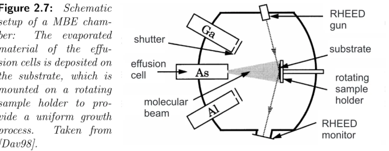
Epitaxial growth of heterostructures is realized by a radiation of the substrate with molecular beams from heated effusion cells (see Fig. 2.7). The released amount of extra-clean material deposits on the heated GaAs substrate, which is mounted on a rotating sample holder to provide a uniform layer thickness. To avoid any incorporation of random defect atoms, the growth process is enclosed by
10In this work, only 2DES are discussed.
12 CHAPTER 2. BASICS
Figure 2.7: Schematic setup of a MBE cham- ber: The evaporated material of the effu- sion cells is deposited on the substrate, which is mounted on a rotating sample holder to pro- vide a uniform growth process. Taken from [Dav98].
molecular beam effusion cell
shutter
substrate rotating sample holder RHEED gun
RHEED monitor
an ultra-high vacuum chamber supported by a cryogenic cooling shield to freeze out any impurity atoms left. Mechanical shutters in front of the effusion cells ensure the right procedure of epitaxial growth and the performance is simultane- ously controlled by RHEED11 measurements. As a result, the MBE technique is capable of producing samples with an ideal accuracy in the range of single atomic layers and provides therefore the perfect tool to grow ambitious heterostructures.
2.3.1 Sample structure
The whole work is based upon n-doped GaAs/AlGaAs quantum well structures, grown either on a (001)- or a (110)-GaAs substrate. An overview together with some important parameters is given in Tab. 2.1.
sample waver growth width doping densityNs mobility µ name number axis qw (nm) style (1011cm−2) (106cm2/Vs)
A D110831A (001) 12 dsd 5.0 0.22
B C130117A (001) 12 ssd 5.9 0.84
C 7-5-96.1 (001) 25 ssd 2.1 3.37
D D081205A (110) 30 2dsd 3.4 5.10
B∗ C130117A (001) 12 ssd
(gated)
Table 2.1: Investigated samples: The values for the carrier density and the mo- bility in the 2DES were obtained by magneto transport measurements.
The presented values for the electron density and the mobility were deter- mined shortly after the growth process by magneto transport measurements at T = 4.2 K. However, these values may vary to some extent from the one obtained during the Raman measurements. Such an inconsistency may easily be explained by different experimental conditions and will be addressed again throughout the next chapters. In the following, the particular structure of the samples as well as their purpose concerning this work will be elucidated in more detail:
11RHEED: reflection high energy electron diffraction
2.3. INVESTIGATED SAMPLES 13
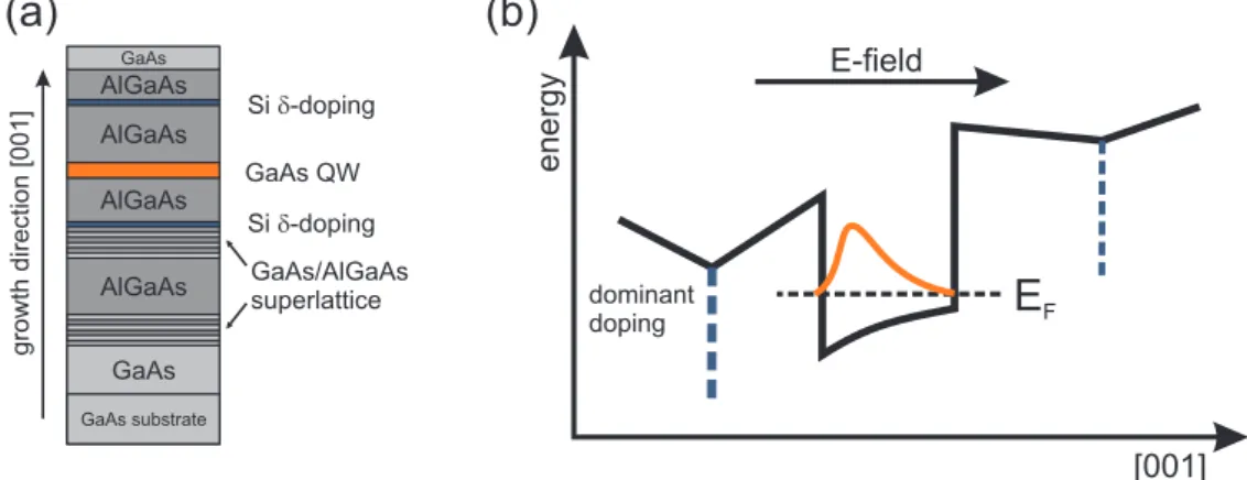
Sample A
Sample A was manufactured in the group of Prof. Dr. W. Wegscheider at the ETH Zurich and was designed to satisfy certain conditions in terms of spin-orbit coupling [Wal12a]. The aim was to achieve a balanced ratio between both contri- butions of the spin-orbit field, yielding a special symmetry called the persistent spin helix. The formation of this interesting phenomenon and the impact on Ra- man scattering will be clarified in detail in Chap. 4. At this point, we will focus mainly on the composition and the basic parameters of the sample.
GaAs/AlGaAs superlattice GaAs QW Si dopingd- Si d-doping
GaAs AlGaAs AlGaAs AlGaAs AlGaAs
GaAs substrate GaAs
growth direction [001]
EF
dominant doping
E-field
[001]
energy
(a) (b)
Figure 2.8: Sample A: (a) Layer composition, not to scale. (b) Asymmetric band profile with a built-in electric field parallel to the growth direction (schematic picture).
The sample is grown on a (001)-GaAs substrate and features a 12 nm-wide single quantum well. A schematic picture with the layer composition and the correspond- ing band profile is shown in Fig. 2.8. Two sequences with GaAs/AlGaAs super- lattices ensure the incorporation of impurity atoms in deeper layers far away from the optical region of interest. Although the structure contains two Si δ-dopings, the band edge profile is not symmetric due to different doping concentrations.
The doping layer on the substrate side dominates the curvature and causes an internal electric field, which pulls the wave function towards the deeper situated interface. A comparatively low electron mobility of µ= 2.2×105cm2/Vs can be explained by the penetration of the wave function into the barrier material and additionally by the location of this dominant doping layer: The epitaxial growth of doping atoms previous to the quantum well may cause a segregation of donor atoms towards the well region, giving rise to an enhanced scattering and hence a low electron mobility in the 2DES [Liu93].
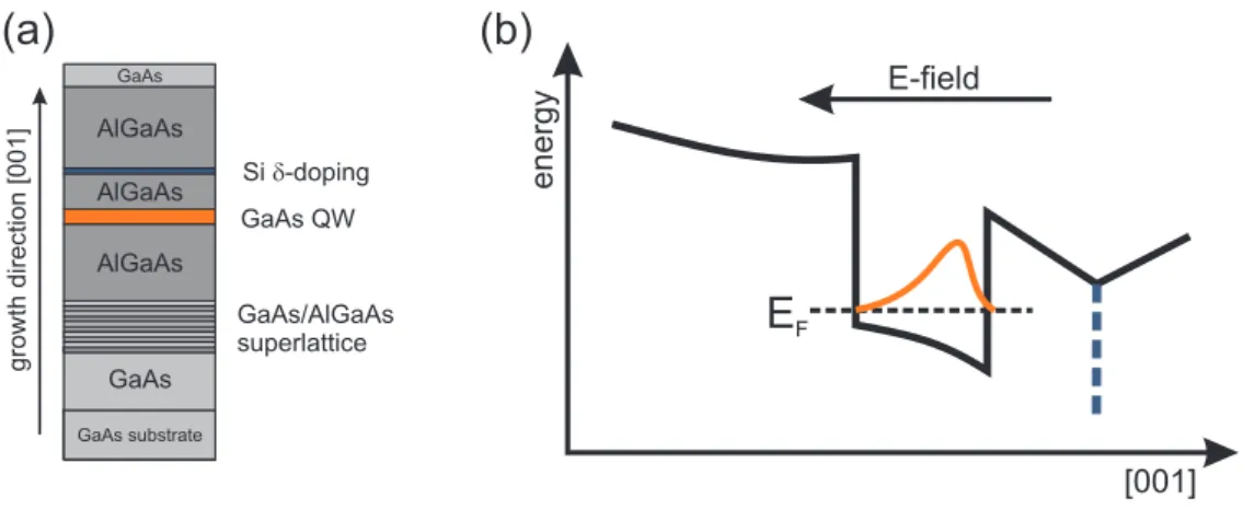
Sample B and B∗
This sample was grown by Dieter Schuh in the group of Prof. Dr. D. Bougeard (University of Regensburg) and was basically intended to provide similar con-
14 CHAPTER 2. BASICS
ditions concerning spin-orbit fields as sample A. Therefore, again a 12 nm-wide GaAs quantum well, surrounded by AlGaAs barriers, is grown on a (001)-oriented substrate (see Fig. 2.9). The significant difference between these two samples is the reduction to a single δ-doping, located between the quantum well and the surface. This doping layer establishes an electric field pointing towards the sub- strate, causing a kind of mirrored band edge profile with respect to sample A.
The nominal electron density of Ns = 5.0×1011cm−2 is just slightly higher than the one for the dsd quantum well. However, the mobility is increased by almost a factor of 4, probably favored by the single-sided doping. This difference will play a significant role in Chap. 6, where the cyclotron motion in an external magnetic field is of great importance.
GaAs/AlGaAs superlattice
GaAs QW Si d-doping
GaAs substrate GaAs
growth direction [001]
E-field
[001]
energy
(a) (b)
EF GaAs
AlGaAs AlGaAs AlGaAs
Figure 2.9: Sample B: (a) Layer composition, not to scale. (b) Asymmetric band profile with a built-in electric field antiparallel to the growth direction (schematic picture).
Sample B∗ stems from the same waver as sample B, but was provided with a semi-transparent top gate to investigate the influence of an external electric field on the band structure. A detailed description of the gating process is given at the end of this section, while the experimental results are presented in Chap. 3.2.2 and Chap. 4.2.6.
Sample C
This heterostructure is also grown on a (001)-substrate, but contains a single qw with a well width of 25 nm. Since the doping layer is integrated in the barrier on the surface side of the 2DES, the band edge profile can be pictured similar to sample B. The larger quantum well causes a distinct reduction of the spacing between the subbands in the electron gas. Therefore, this sample is employed to clarify the fundamental concepts of intersubband excitations in a quantum well structure and to elaborate on the distinctions between different well sizes, which is discussed in Chap. 3.2.
2.3. INVESTIGATED SAMPLES 15
Sample D
Modern growth schemes, like the one proposed in [Uma09], paved the way to extremely high electron mobilities in semiconductor heterostructures. A crucial impact is given by the shape of the band edge profile, which is depicted for sample D in Fig. 2.10. This heterostructure features a 30 nm-wide quantum well, oriented in (110)-direction. Four symmetrically arranged doping layers cause the electron wave function to center in the middle of the quantum well, minimizing the pene- tration into the low-mobility material and mostly preventing the scattering due to interface roughness. A further feature of the depicted structure is the distribution of the doping amount: The flat band profile within the barriers is realized by a fairly high sheet density of silicone in the far-off dopings, while the doping lay- ers close to the quantum well are responsible for the carrier concentration in the 2DES. A high mobility is additionally facilitated by the lower growth tempera- ture compared to (001)-structures, preventing the doping atoms to segregate into the quantum well region [Bel08]. However, not the mobility, but the vanishing internal electric field, caused by the symmetric doping arrangement, is of great interest for this work. To this end, Chap. 4.3 is dedicated to reveal the effect on the band structure.
[110]
energy
E
FSi d-doping
Si d-doping
Figure 2.10: Sample D: Symmetric band profile with vanishing electric field due to four symmetric doping layers (schematic picture).
2.3.2 First characterization: PL and PLE
The size of the band gap is an important quantity in the spectroscopy of semi- conductors, providing a first approximation how much energy is needed to lift an electron from the valence band to the conduction band. An experimental approach is given by photoluminescence (PL) spectroscopy, where electron-hole pairs are generated by an excitation with a laser energy above the band gap (see Fig. 2.11). Due to intrasubband scattering events, the generated charge carriers relax on a very fast timescale towards the band extrema, where they recombine irradiantly under the conservation of energy and momentum. The excitation and recombination processes in the E(k) diagram are assumed to be vertical, since the k-vector of photons is negligible. Considering doped systems, transitions from
16 CHAPTER 2. BASICS
k E(k)
HH
LH EF
EG
luminescence
optical excitation non radiative relaxation
conduction bandvalence band
Figure 2.11: Schematic picture of the photoluminescence in k-space.
Figure 2.12: PL spectra for all inves- tigated samples.
k = 0 to k =kF (Fermi wave vector) contribute to photoluminescence, resulting in a typical shark-fin like shape of the spectra (see, e. g., sample C in Fig. 2.12).
Because the heavy hole states in the valence band feature a large effective mass, the curvature of this band is very flat and hence, the dispersion of the conduction band mainly determines the spectral width of a PL trace.
The measured photoluminescence of each sample at T = 5.5 K is plotted in Fig. 2.12 and the extracted values for the size of the band gap can be found in the inset. A first tendency is rapidly perceived, saying a larger quantum well width results in a lower band gap energy. Comparing sample A and B, which contain nominally the same qw width of 12 nm, one would expect a very similar transition energy in the first place. The given discrepancy may be explained by different band bendings or the variation of the actual quantum well size throughout the wafer, manifesting itself in a huge deviation up to ≈4 meV in the transition en- ergy for different samples of the same wafer. In consequence, all measurements were carried out on the same samples to provide a comparability of results12. A further origin of the redshift in sample B may be attributed to the band gap renormalization (BGR), which denotes a reduction of the gap size scaling with in- creasing carrier density and decreasing quantum well width [Kle85, DS90, Haa92].
Assuming a similar qw width, a lower transition energy of sample B would there- fore be governed by the higher carrier density in the 2DES. However, this effect is probably very small since both carrier densities are of comparable magnitude.
A vague indication of the carrier density is already provided by the linewidth
∆E = EF −EG of the PL trace [Gri12a], but a further approximation is spared here for the following reasons: Although the shark-fin shape is clearly visible for sample C and D, the Fermi edge is hardy recognizable for the samples with a higher carrier density (sample A and B). The contrast may be increased by choos- ing a logarithmic scale (not shown), however, this estimation would still contain
12Sample B∗ is from the same waver as sample B, but a different fraction. Otherwise the results of sample B would not be reproducible. Therefore, a slight deviation of these two samples in the main parameters may be present.
2.3. INVESTIGATED SAMPLES 17
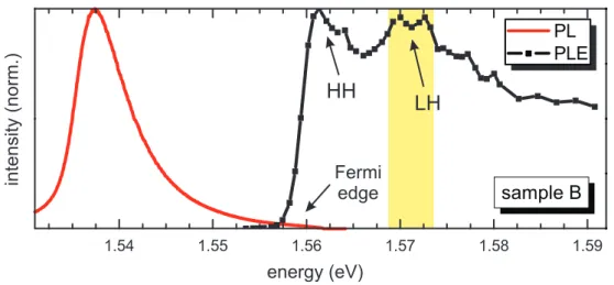
Fermi edge
HH LH
energy (eV)
intensity (norm.)
Figure 2.13: PL and PLE measurement of sample B. The absorption of the 2DES starts in the vicinity of the Fermi edge. The yellow shaded region represents the mainly used excitation energy for measurements on intrasubband transitions.
a huge inaccuracy. Furthermore, the carrier density of the 2DES can be extracted directly from the results on Raman scattering in this work, yielding a more precise approach of the actual value during the measurements.
So far we only considered the fundamental band gap and the impact of the Fermi energy, but for inelastic light scattering in a 2DES, also the subband structure of the valence band plays an important role due to resonance effects. A common way to probe the absorption of a quantum well system is the photoluminescence excitation spectroscopy (PLE), where PL traces are measured for different excita- tion energies. The amplitude of the single spectra can be extracted and provides an indication of the absorption in the quantum well. Figure 2.13 exemplarily shows the PLE spectrum of sample B together with its photoluminescence. An absorption of light does not start until the laser energy overcomes the band gap as well as the Fermi energy. For higher excitation wavelengths, the quantum well remains transparent. The absorption line in the vicinity of the Fermi edge can be attributed to the transition from the HH band, while the resonance with the LH states is blue shifted by ≈10 meV. Usually, Raman excitations aspire a resonant intermediate state. Hence, most measurements of this work, especially concerning intrasubband transitions, are carried out with an excitation energy in the yellow shaded region and exploit the resonance with the LH valence band.
2.3.3 Fabrication of an electrical gate
As we already discussed in this chapter, the band edge profile in the vicinity of the quantum well is mainly influenced by the electric field. The internal field is basically determined by the incorporation of the modulation doping, but now we introduce a way to apply an additional field by means of an external gate, which allows us to manipulate the total electric field strength of the 2DES to some degree.
18 CHAPTER 2. BASICS
Figure 2.14: Sample with a semi- transparent top gate. Thin gold wires are used to connect the 2DES and the gate contact with the contact pads of the sample holder.
Figure 2.15: I-V characteristic of sam- ple B∗ with a typical diode like behav- ior. Setting a limit of ±100µA, the gate voltage can be tuned between -6 V and +16 V.
At the beginning of the fabrication process, the sample is cleaned by sonication in acetone, ensuring a deposit-free surface. Afterwards, a diamond tip scratcher is used to implement a small scratch in each corner of the surface, where a small amount of indium is deposited with a clean soldering rod. To conclude this step, the indium has to be alloyed into the crystal, building an electric contact between the drop at the surface and the 2DES. For that reason, the sample is enclosed in forming gas atmosphere and heated within 60 s to 350◦, where it remains for additional 60 s.
After the sample is cooled down, it is equipped with an appropriate mask and mounted in the high vacuum evaporation chamber. For all-optical measurements like inelastic light scattering, the semi-transparency of the top gate is of crucial interest. Therefore, a nickel-chromium (NiCr) alloy is used, yielding a transmis- sion of about 70% for a nominal 6 nm thick layer (see Fig. 2.14).
In the next step, the sample is glued by conductive silver to a previously pre- pared sample holder, where contact pads are equipped by enameled copper wires with plug-in IC pins. Finally, all alloyed contacts in the corners as well as the top gate, where tiny drops of conductive silver are used, are connected by thin gold wires to the contacts pads. The functionality of the contacts is subsequently checked by simple resistance measurements between each contact.
Typical values for sample B∗ at room temperature were about 3 - 5 kΩ between contacts of the 2DES and about 50 kΩ between both top gate contacts. Figure 2.15 shows the determined I-V characteristic for sample B∗ at liquid helium temper- ature. Since the shape of the curve has a diode-like behavior, the current was restricted to±100µA in order to prevent the sample from suffering any damage.
This limited the operating voltage of the gate to a range of −6 V to +16 V.
2.4. INELASTIC LIGHT SCATTERING 19
2.4 Inelastic light scattering
The inelastic light scattering was experimentally invented by the Indian physi- cist Chandrasekhara Venkata Raman, who was awarded for his discovery in 1930 the Nobel price in physics. Ever since then, the so called Raman scattering is employed in wide fields of chemistry and physics as a non-destructive method to investigate fundamental excitations in materials. From a historical point of view, the Brillouin scattering, where acoustic phonons are excited, can be dis- tinguished from the classical Raman scattering, where only optical phonons or internal vibrations of molecules contribute to the scattering [Sch06]. Nowadays, this technique is indispensable for the characterization of modern layered crystal structures as graphene [Fer06, Hey10] or MoS2[Lee10, Ple12]. But the application of Raman scattering is not limited to phonons in a medium. Electronic excitations of semiconductors, as depicted in this work, are also covered by this technique, which is often called inelastic light scattering in that context. This makes Raman scattering a timeless tool with various applications in the latest research fields.
2.4.1 General concept
The basic principle of Raman scattering can be understood in a simple picture as follows: An incoming photon with the energy ~ωI and the momentum kI causes either a creation (Stokes process) or an annihilation (anti-Stokes process) of an elementary excitation with the energy ~ω and the momentum q. According to the conservation law, the energy of the scattered photon is given by
~ωS =~ωI±~ω , (2.12)
where the plus (minus) sign is for the anti-Stokes (Stokes) process. As a conse- quence, the scattered photon is shifted to higher and lower energies, respectively.
Moreover, the conservation of momentum determines
kS =kI±q, (2.13)
with the same correlation of signs. A schematic picture of these scattering events is depicted in Fig. 2.16. The detection of the scattered photons yields important information about the energy and the momentum of the investigated excitations in the medium.
Figure 2.17 illustrates a typical Raman spectrum with an excitation energy of
~ωI. The elastically scattered light, which stems for instance from the sample surface, is visualized as the dominant contribution in the center of the spectrum.
Since all measurements in this work are carried out at very low temperatures (≈ 5.5 K), there hardly exist any excitations in the semiconductor system and hence, only the Stokes process plays an important role. However, Chap. 5 is dedicated to discuss briefly the occurrence of the anti-Stokes component in the examined heterostructures.
20 CHAPTER 2. BASICS
wII,k wS,kS
w,q
wII,k wS,kS w,q
Stokes
anti-Stokes
Figure 2.16: Schematic picture of the Stokes and the anti-Stokes process.
intensity
energy
wI - w wI wI + w
Stokes anti-Stokes
Figure 2.17: Schematic picture of a Raman spec- trum. The Stokes process is shifted to lower, the anti-Stokes to higher energies.
In experimental spectra, the energy of elastically scattered light is usually set as the zero point and the Stokes component covers the positive side of the x-axis.
This convention will be kept throughout the work. Furthermore it is mentioned that the Raman scattering amplitude is exceeded by the signal of the elastically scattered light by far.
One of the striking benefits of Raman scattering, and also a crucial element for this work, is the ability to transfer a particular wave vector q to the excitation.
An exact backscattering geometry, where the directions of incoming and scattered light are antiparallel and perpendicular to the sample surface, yields the maximum value for the transferred wave vector [Sch06]:
qmax = 4π
λI (2.14)
q q
kIkS
Figure 2.18: Backscattering geometry with a transferred wave vector q.
Here, the assumption of approximately equal in- coming and scattered wavelengths (λI ≈ λS) is thoroughly valid, considering the small energy of the excitation compared to the incident laser en- ergy.
For quantum well structures, a further discus- sion on the momentum transfer is necessary: Since the translational symmetry is not conserved in the growth direction, the momentum can only be trans- ferred in lateral directions of the 2DES. Conse- quently, the wave vector parallel to the quantum well plane may be adjusted continuously by
q= 4π
λI sin(θ), (2.15)
2.4. INELASTIC LIGHT SCATTERING 21
while an equal angle θ for incident and scattered light is assumed (see Fig. 2.18).
Because such a configuration is used in numerous measurements of this work, the formula is of great interest and will be used throughout the following chapters.
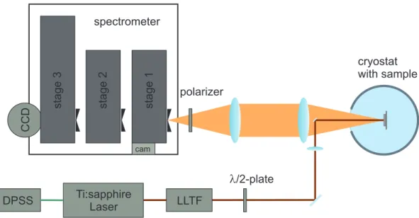
2.4.2 Experimental setup
All experimental data presented in this work are obtained with a typical Raman setup, which allows photoluminescence and Raman measurements in backscatter- ing geometry. A schematical picture of this setup is illustrated in Fig. 2.19.
DPSS Ti:sapphire Laser
stage 3 stage 2 stage 1
CCD
cam
l/2-plate polarizer
cryostat with sample spectrometer
LLTF
Figure 2.19: Experimental setup of the Raman lab used in this work.
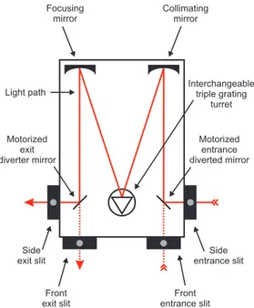
The laser light is provided by a continuous wave (cw) titanium-sapphire laser (TiSa), which is pumped by a diode-pumped solid state laser (DPSS). Although the possible tuning range of the TiSa covers 620 to 1000 nm, all presented mea- surements were conducted with a wavelength between 730 and 820 nm. After the laser beam is emitted, it is guided into a laser line tunable filter (LLTF). This device is based on the Bragg filter technology and allows a laser line selection with a quite narrow bandwidth (FWHM≈ 0.3 nm), enabling a detection of Ra- man excitations with energies as low as 0.3 meV. Before the beam is coupled into the cryostat, the polarization can be varied by aλ/2 plate. The linearly polarized laser light is then focused onto the sample with a spot size diameter of about 100µm and a power density attenuated to about 80 W/cm2. Two sizable achro- matic lenses are functionalized to gather and focus the scattered light into the triple stage Raman spectrometer. A polarizer in front of the entrance slit may select the requested polarization of the scattered light. The spectrometer consists of three individually adjustable stages, assembled to separate the elastically scat- tered laser light from the low-intensive Raman signal. For this purpose, the first two stages are utilized as a tunable bandpass13, while the third stage yields the
13For a fixed laser wavelength, the first two stages may be substituted by filter foils. However, a tunable bandpass is indispensable for a tunable laser system as used in this setup.
22 CHAPTER 2. BASICS
S1
S1,2
S2,3
G1
G2
G3
Figure 2.20: Subtractive mode of the triple stage Raman spectrometer: The first two stages act as a variable band- pass to filter the interfering stray light from the Raman signal. The spec- tral resolution is afterwards gained by the grating in the third stage, project- ing the scattered light on a CCD-chip which is read out by a computer.
Collimating mirror Focusing
mirror
Light path
Motorized exit diverter mirror
Side exit slit
Front exit slit
Front entrance slit
Side entrance slit
Motorized entrance diverted mirror Interchangeable
triple grating turret
Figure 2.21: Schematical composition of a single stage: The beam is guided through the entrance slit and mirrored onto a changeable grating, where the light is spectrally split and merged, re- spectively, before it is decoupled by the exit slit. Additional front slits allow the operation of assistant devices like video cameras or adjustment lasers.
actual spectral resolution (see Fig. 2.20 and Fig. 2.21), which was about 34µeV in all measurements. The spectra of the scattered light was finally detected by a liquid-nitrogen-cooled CCD14-chip and sent to a computer.
According to the aim of the measurement, two different cryostats could be integrated into the experimental setup: In the flow cryostat, depicted in Fig. 2.22, the sample is surrounded by helium gas, ensuring an ideal cooling efficiency of the 2DES. In fact, the temperature could be cooled down to liquid helium temperature (T ≤ 4.2 K), however, a slightly increased temperature of 5.5 K was constantly selected to prevent the light from scattering on occasionally appearing air bubbles in the liquid phase. The sample is here mounted on a rotatable sample holder, giving rise to a quasi continuously tunable wave-vector transfer to the 2DES. This configuration allows measurements with a tilt angleθ up to≈ 60◦, corresponding to qmax ≈ 13.8×10⁶m−1 for an excitation wavelength of 790 nm. Additionally, an aperture was used to restrict the inaccuracy of the scattering angle to ±4◦.
For measurements with an external magnetic field, the cryostat sketched in Fig. 2.23 was used. Herein, the sample was mounted on a coldfinger, which is coupled by a heat exchanger to the liquid helium. Although the nominal sample temperature displayed ≈ 4 K, the actual temperature of the 2DES was consid-
14CCD: charge-coupled device
2.4. INELASTIC LIGHT SCATTERING 23
2DES
sample q
laser lens
aperture spectro-
meter q
Figure 2.22: Top view of the flow cryostat: A rotatable sample holder enables a quasi continuously-tunable wave-vector transfer to the 2DES. The surrounding helium gas ensures a de- cent and constant cooling of the elec- trons in the quantum well.
laser spectro- lens meter
q B B
B 2DES
wires
Figure 2.23: Top view of the magnetic field cryostat: The sample is mounted on a fixed coldfinger, providing a cer- tain wave-vector transfer. The en- casing solenoid establishes a magnetic field with a component parallel and perpendicular to the qw plane.
erably higher (up to ≈ 20 K) due to the weak cooling power of the system. To provide a certain wave vector in the quantum well plane, small attachments with a fixed slope could be incorporated to the sample holder. The magnetic field is provided by a superconducting solenoid, capable of field strengths up to 5 T. Since the sample is mounted in a certain tilt angle, the total magnetic field splits up into a component parallel and a component perpendicular to the quantum well plane. An additional restriction of the scattered light is not needed due to the low built-in aperture angle of this cryostat.
Chapter 3
GaAs/AlGaAs quantum wells:
Fundamental concepts
3.1 Electronic elementary excitations
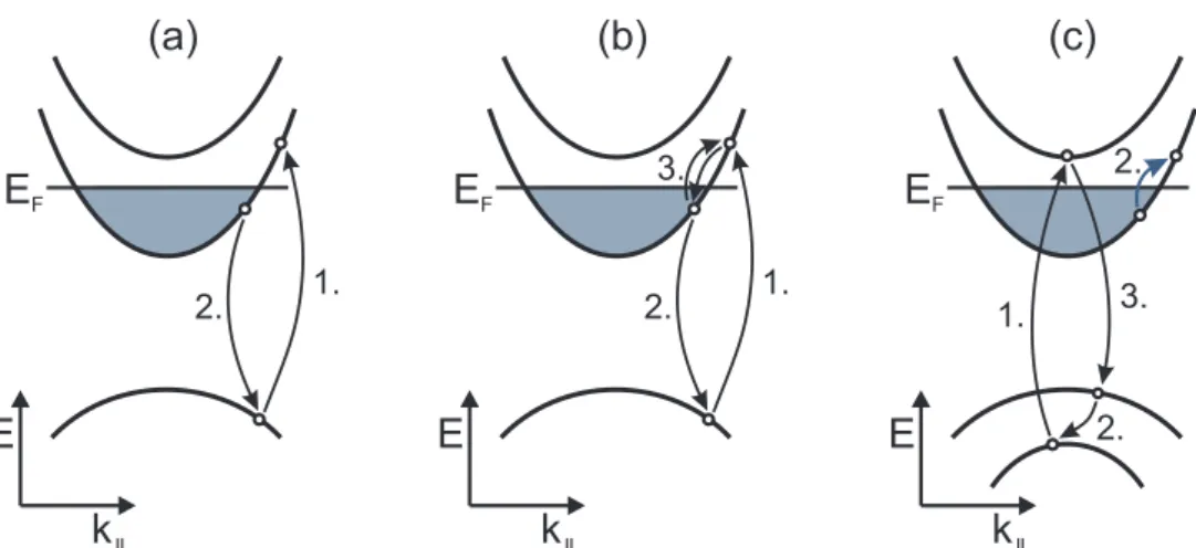
Inelastic light scattering is a powerful tool to investigate the electronic elementary excitations in semiconductor nanostructures. Those excitations can be categorized into three different groups: Charge- (CDE) and spin-density excitations (SDE), which count among the collective electron modes, and the historically labeled single-particle excitations (SPE). While SPE reflect only discrete transitions in a non-interacting single-particle picture, collective excitations take direct- and exchange-Coulomb interactions into account and hence are shifted to higher and lower energies, respectively. In the following, these elementary excitations will be introduced in detail.
3.1.1 Single-particle continua
The nature of the single-particle excitations was for a long time thought to be not affected by Coulomb interactions, but has been controversially discussed over years. In fact, these excitations are subjected to a collective nature as well [DS99, Sch06], but since their energies are close to single-particle transitions, the excitations are treated and labeled as SPE further on.
Considering a simplified picture of non-interacting particles in a 2DES, the possi- ble excitations from the Fermi sea include intersubband transitions between dif- ferent energy subbands and intrasubband transitions within an occupied subband.
Such a situation with selected excitations is illustrated in Fig. 3.1. While inter- subband transitions, represented by solid arrows, occur either vertically (q= 0) or tilted (q6= 0) in the dispersion relation, a finite wave-vector transfer is indis- pensable for transitions within a single subband (dotted arrow). A so called single-particle continuum is then formed by regarding all possible SPE for every transferred wave vector q. Figure 3.2 shows the continua for the first two sub-
25
26 CHAPTER 3. GAAS/ALGAAS QUANTUM WELLS: FUNDAMENTAL CONCEPTS
E
k , k
x yq=0
q2 EF
E0
E1 E2
q1
Figure 3.1: Schematic picture of single-particle excitations in a 2DES.
Intersubband and intrasubband transi- tions are indicated by solid and dotted arrows, respectively. The subbands are described by a paraboloid in the kx-ky plane.
E E
01q
0 1
0 0
q
1q
2intersubband
intrasubband
Figure 3.2: Single-particle continua formed by the parabolic behavior of the conduction bands. Selected intra- and intersubband transitions of the first two subbands are marked. The contin- uum for transitions to the E2 subband is not shown here.
bands15 together with a qualitative localization of the excitations from Fig. 3.1.
The upper edge of the intrasubband continuum can be determined in a parabolic approximation of the conduction bands as
E(kF +q)−E(kF) = ~2(kF +q)2
2m∗ − ~2kF2
2m∗ = ~2qkF
m∗ + ~2q2
2m∗ ≈ ~2qkF
m∗ , (3.1) assuming a rather large Fermi wave vector kF compared to the transferred wave vector q [Sch06]. As indicated in the schematic picture, the two-dimensional subbands are described by rotational paraboloids in thekx-ky-plane, giving rise to intrasubband transitions with infinitesimally small energies starting at the Fermi edge up to any point of the paraboloid. Consequently, the lower edge of this continuum is approximately zero for all q <2kF. For intersubband transitions (here: E0→E1), the edges of the continuum are given by
E01+E(kF ±q)−E(kF) = E01± ~2qkF
m∗ +~2q2
2m∗ , (3.2)
with the subband spacingE01 =E1−E0for each selected inplane wave vectorkk = (kx, ky). Considering only vertical transitions, a discrete spectrum of intersubband excitations with equal energy spacing is obtained. However, transferring a certain wave vectorqto the system, the carrier densityNsof the Fermi sea may be derived from intrasubband transitions by means of Eq. (3.1) and the relation
kF =p
2πNs . (3.3)
15The intersubband transition fromE0 toE2 is therefore not shown in Fig. 3.2.
3.1. ELECTRONIC ELEMENTARY EXCITATIONS 27
An application of this carrier-density determination will be presented in Chap. 4, where we focus on the intrasubband excitations of the investigated samples.
3.1.2 Collective charge- and spin-density excitations
The above introduced SPE are based on the principle of non-interacting particles, but collective effects may not be neglected in a 2DES. A response of the Fermi sea to a single electron transition can cause an energetic shift of the excitation according to interaction effects of the charge carriers. We will continue this dis- cussion by means of an actual Raman spectrum, obtained without a transferred wave vector (q∼= 0).
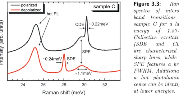
Figure 3.3: Raman spectra of intersub- band transitions in sample C for a laser energy of 1.57 eV.
Collective excitations
(SDE and CDE)
are characterized by sharp lines, while the SPE features a broad FWHM. Additionally, a hot photolumines- cence can be identified at lower energies.
Figure 3.3 shows the intersubband transitions of sample C and is obviously more complex as expected from the considerations in the previous section. The SPE at the bare subband spacing E01 was supposed to exhibit a sharp transition energy, but manifests itself as a broad feature in the excitation spectra. Furthermore, the SPE is enclosed by narrow peaks which can be ascribed to collective modes of the Fermi sea. Those charge- and spin-density excitations appear only in polarized and depolarized spectra, respectively, and are asymmetrically shifted against the energy of the single-particle transition. Here, we already make use of the polar- ization selection rules, which will be introduced in Chap. 3.1.4 in more detail.
Additionally, a photoluminescence from a higher subband, so called hot PL, is detected at lower energies.
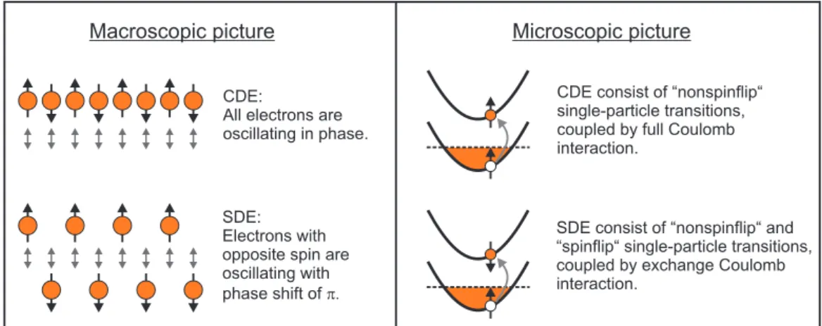
A phenomenological description of the collective modes is presented in Fig. 3.4.
Macroscopically, an intersubband CDE of a 2DES is an in-phase oscillation of electrons perpendicular to the quantum well plane. The motion of the oscillating charge carriers is restricted by the interfaces of the quantum well. Going to micro- scopic scales, the intersubband CDE is a spin-conserving single-particle transition, which is subjected to the full quantum-mechanical Coulomb interaction [Sch06].
By contrast, the intersubband SDE embodies an opposite phase oscillation for